

QUAD-QUAD-MXFE HDL project
This reference design is not tested in hardware but in testbench. It should serve as a reference for building systems with multiple channels, e.g., 128 ADC channels and 128 DAC channels or more, realized with AD9081 parts.
Supported devices
Supported carriers
None — built on top of VCU128 but does not match any FMC connector due to the high number of lanes. The design requires 64 lanes for Rx and 64 lanes for Tx, but the FMC+ connector can expose only 24 pairs instead of 64.
Software support
Software support for other MxFE projects:
Quad-MxFE Software Quick Start Guide
Block design
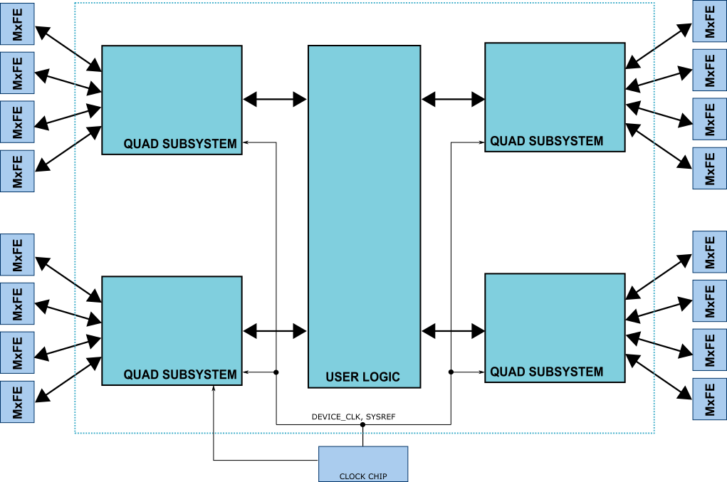
The block design consists of four “quad JESD subsystem” block components, where each quad block services four Rx/Tx link pairs. Each link pair connects to an AD9081 MxFE chip, where each MxFE chip has 8 ADC and 8 DAC channels. In turn a quad block services a total of 32 ADC and 32 DAC channels.
Having four quad MxFE blocks in parallel gives us 128 ADC and 128 DAC real channels at the transport layer, or 64 complex ADC channels and 64 complex DAC channels.
All quad blocks share a common device clock and SYSREF signal to ensure that samples are aligned at application layer across all channels.
Quad JESD Subsystem
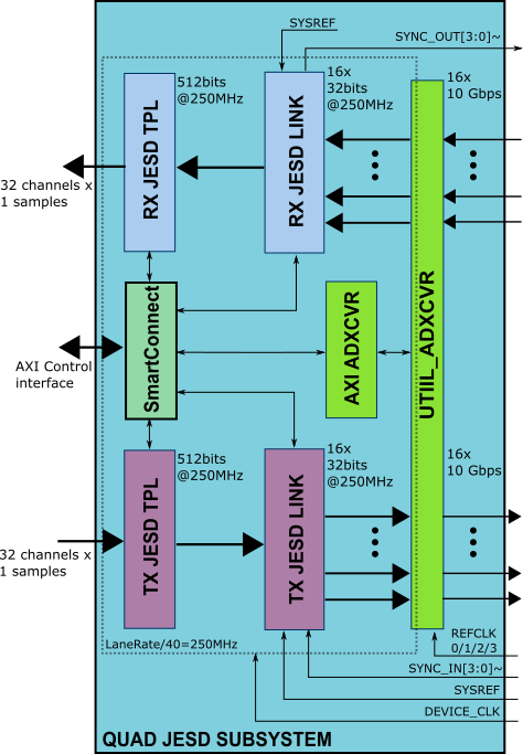
Each quad block contains all components required to handle the JESD link from physical layer to transport layer. The block exposes at its interface raw sample channel streams the user logic can be connected to. The format of the channels is one sample per channel per clock cycle.
A smart interconnect block is added to distribute the control interface to all JESD peripherals. This would lead to better partitioning of the overall design helping the routability and timing closure.
JESD Link settings
For each quad JESD subsystem the Rx link (ADC Path) operates with the following parameters:
JESD204 8b/10b link layer (‘204B’ mode)
Rx Deframer parameters: L=4, M=8, F=4, S=1, N’=16, N = 16 (equivalent to Quick Config 0x0A)
Number of links : 4
Dual link : No
DEVICE_CLK – 250 MHz (Lane Rate/40)
REF_CLK – 500 MHz (Lane Rate/20)
Lane Rate – 10 Gbps
QPLL0 or CPLL
For each quad JESD subsystem the Tx link (DAC Path) operates with the following parameters:
JESD204 8b/10b link layer (‘204B’ mode)
Tx Framer parameters: L=4, M=8, F=4, S=1, N’=16, N = 16 (equivalent to Quick Config 0x09)
Number of links : 4
Dual link : No
DEVICE_CLK – 250 MHz (Lane Rate/40)
REF_CLK – 500 MHz (Lane Rate/20)
Lane Rate – 10 Gbps
QPLL0 or CPLL
Resource utilization per quad subsystem
The transport layer cores have optional features (e.g. DDS) which can be disabled through synthesis parameters that can impact significantly the resource utilization of the subsystem. Below you can observe the impact of the DDS cores on the utilization.
Device Family |
DDS |
CLB LUTs |
CLB Registers |
XCVR Lanes |
|---|---|---|---|---|
Xilinx Virtex US+ |
Yes |
68535 |
86163 |
16 |
Xilinx Virtex US+ |
No |
20332 |
29426 |
16 |
Addressing timing closure issues
Additional pipeline stages can be enabled in the link layer NUM_INPUT_PIPELINE parameter for the link receive peripheral or NUM_OUTPUT_PIPELINE parameter on the link transmit peripheral. This will break the timing arc between the link layer and physical layer and allow a more relaxed placement of the cores.
Clocking
The reference clock for each transceiver quad is exposed in the top level file. The reference clocks should be connected to all ports. If there is no reference clock connected to a specific quad, the reference clock for the quad above or below should be used. If that’s not available also, the reference clock for the quad +2 (above the one above) or quad -2 (below the one below) should be used. The overall clock tree for the system (single FPGA or multi FPGA) should ensure all reference clocks are derived from the same crystal. Phase is not important for the reference clocks.
Requirements
Below are quoted few of the most important guidelines from the JESD standard. For more details consult the standard.
“All device clocks in the system shall be phase locked to a common source.”
“The device clock and SYSREF signal to each device should be routed close to each other”, or length matched.
“It is strongly recommended to use the same type of signal type for SYSREF and the device clock, to maintain an accurate timing relationship.”
“Transmission skew: The skew contribution due to the different propagation delays in the transmission medium for different lanes. Maximum of 4 ns propagation delay difference between lanes which corresponds e.g., to a lane length difference of 56 cm for stripline on an FR-4 board with ER=4.5. Larger lane length differences will not be likely in a JESD204 system.”
Restriction/requirement particular to the current implementation using the JESD framework:
All four lanes within a link must be mapped in a way so they connect to a single transceiver quad, order within the transceiver quad is not relevant.
All transceiver quads must have access to a reference clock, connected to the MGTREFCLK pin of the same quad or to adjacent quads. The reference clock frequency should match across all transceiver quads but it does not have to be phase aligned.
SYSREF signals connected to all MxFEs should be length matched
Device clocks connected to all MxFEs should be length matched
Resources
More information
Support
Analog Devices will provide limited online support for anyone using the reference design with Analog Devices components via the EngineerZone.