User Guide - Electrical Specifications
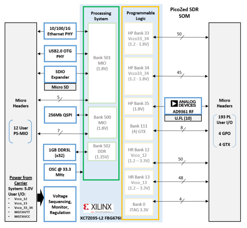
Designing with the AD9361-Z7035 2X2 SOM requires an understanding of the system I/O that are available, how they are powered, and where the signals connect on the SOM. Those details are covered in the remaining sections. This diagram shows a summary of all system peripherals and user I/O available.
Xilinx Zynq-7000 All Programmable SoC
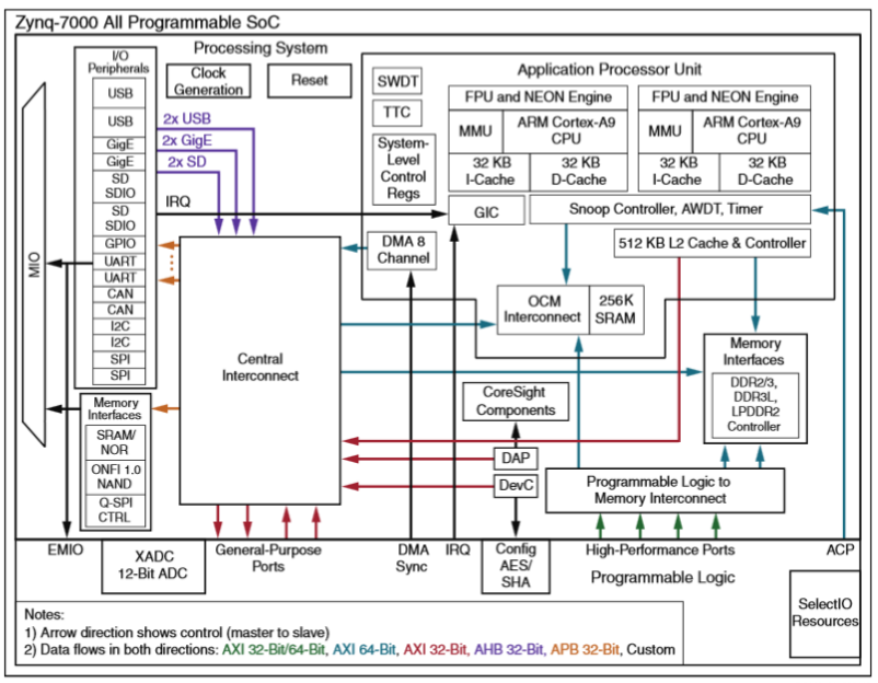
AD9361-Z7035 2X2 includes a Xilinx Zynq XC7Z035-L2 FBG676I AP SoC. Tight integration between the ARM-based processing system and the on-chip programmable logic creates unlimited possibilities for designers to add virtually any peripheral or create custom accelerators that extend system performance and suit unique application requirements.
This is a -2 speed grade and low power (-L) binned device. All SOM memory and digital interfaces connect to Zynq through the Processing System (PS) or Programmable Logic (PL). The Analog Devices AD9361 connects through Zynq PL.
Consult the Xilinx Zynq-7000 AP SoC Technical Reference Manual for more information: https://www.amd.com/content/dam/xilinx/support/documents/data_sheets/ds190-Zynq-7000-Overview.pdf
Analog Devices AD9361 RF Agile Transceiver
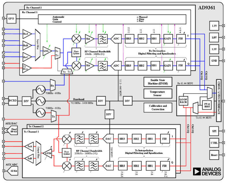
AD9361-Z7035 2X2 includes an Analog Devices AD9361 RF Agile Transceiver™. The AD9361 is a high performance, highly integrated RF Agile Transceiver™. Its programmability and wideband capability make it ideal for a broad range of transceiver applications. The device combines an RF front-end with a flexible mixed-signal baseband section and integrated frequency synthesizers. The AD9361 operates in the 70 MHz to 6.0 GHz range, covering most licensed and unlicensed bands. Channel bandwidths from less than 200 kHz to 56 MHz are supported.
Consult the AD9361 Reference Manual UG570 for more details.
AD9361/Zynq SoC Connection
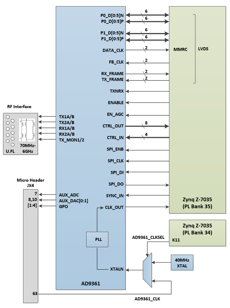
AD9361-Z7035 2X2 connects the Xilinx Zynq Z-7035 SoC directly to the AD9361 RF Agile Transceiver with dedicated high bandwidth data ports and clocks, an SPI control interface, and other control and framing signals.
The AD9361 digital interface is comprised of two parallel data ports (P0 and P1) and several clock, synchronization, and control signals to transfer samples between the AD9361 and the Zynq SoC. These signals can be configured as single-ended CMOS signals or as Low Voltage Differential Signal (LVDS, ANSI-644 compatible) signals for systems that require high speed, low noise data transfer. The system level reference designs that exist for the AD9361-Z7035 all use LVDS, to achieve the maximum data throughput, but can be configured in CMOS mode to better prototype a different hardware subsystem.
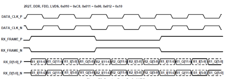
In LVDS mode, the interface is operated in double-data rate (DDR) mode. Therefore, 12-bit samples to/from the AD9361 are sent across two 6-bit lanes on differential pairs.
Maximum rate across the Zynq-AD9361 data interface is limited by AD9361 max data rate (122.88MSPS).
The timing diagram below is included for illustration of the data interface. Consult the AD9361 Reference Manual for more details.
Analog Devices provides Zynq HDL source code and Linux drivers for the AD9361. Designers are encouraged to reuse them. More information can be found at their AD9361-Z7035 page.
Memory
Zynq contains a hardened PS memory interface unit. The memory interface unit includes a dynamic memory controller and static memory interface modules. AD9361-Z7035 takes advantage of these interfaces to provide system RAM as well as non-volatile memory.
DDR3
AD9361-Z7035 includes two Micron MT41K256M16HA-125 DDR3L low power memory components creating a 256M x 32-bit interface, totaling 1 GB of random access memory. The DDR3L memory is connected to the hard memory controller in the PS of the Zynq AP SoC. The PS incorporates both the DDR controller and the associated PHY, including its own set of dedicated I/Os.
Speed of up to 1,066 MT/s for DDR3L is supported.
The DDR3L interface uses 1.35V SSTL-compatible inputs by default.
DDR3L termination is utilized on AD9361-Z7035 and configured for fly-by routing topology, as recommended in Xilinx UG-933. Additionally the board trace lengths are matched, compensating for the XC7Z035- FBG676 internal package flight times, to meet the requirements listed in the Zynq-7000 AP SoC PCB Design and Pin Planning Guide UG-933.
The Zynq digitally controlled impedance (DCI) reference resistors (VRP/VRN) are 240Ω. The differential clock DDR3_CK pair is terminated with 80Ω. The DDR3-CKE0 is terminated through 120 ohms to VTT_0P75. The DDR3-ODT has the same 120 ohm to VTT_0P75 termination. This implementation departs from the Xilinx recommendations in UG933. Termination values for AD9361-Z7035 are based on data from Micron and chosen to significantly reduce power consumption. Each DDR3 chip has its own 240-ohm pull-down on ZQ.
Note: DDR-VREF is not the same as DDR-VTT.
DDR3 Connections
Signal Name |
Description |
Zynq AP SOC pin |
DDR3 pin |
|---|---|---|---|
DDR_CK_P |
Differential clock output |
R21 |
J7 |
DDR_CK_N |
Differential clock output |
P21 |
K7 |
DDR_CKE |
Clock enable |
U21 |
K9 |
DDR_CS_B |
Chip select |
Y21 |
L2 |
DDR_RAS_B |
RAS row address select |
V23 |
J3 |
DDR_CAS_B |
RAS column address select |
Y23 |
K3 |
DDR_WE_B |
Write enable |
V22 |
L3 |
DDR_BA[2:0] |
Bank address |
PS_DDR_BA[2:0] |
BA[2:0] |
DDR_A[14:0] |
Address |
PS_DDR_A[14:0] |
A[14:0] |
DDR_ODT |
Output dynamic termination |
Y22 |
K1 |
DDR_RESET_B |
Reset |
H22 |
T2 |
DDR_DQ[31:0] |
I/O Data |
PS_DDR_DQ[31:0] |
DDR3_DQ pins [15:0]x2 |
DDR_DM[3:0] |
Data mask |
PS_DDR_DM[3:0] |
LDM/UDM x2 |
DDR_DQS_P[3:0] |
I/O Differential data strobe |
PS_DDR_DQS_P[3:0] |
UDQS/LDQS x2 |
DDR_DQS_N[3:0] |
I/O Differential data strobe |
PS_DDR_DQS_N[3:0] |
UDQS#/LDQS# x2 |
DDR_VRP |
I/O Used to calibrate input termination |
W21 |
N/A |
DDR_VRN |
I/O Used to calibrate input termination |
V21 |
N/A |
DDR_VREF[1:0] |
I/O Reference voltage |
M21, K21 |
VTTREF |
Quad SPI Flash
AD9361-Z7035 features a 4-bit SPI (quad-SPI) serial NOR flash. The Micron N25Q256A11E1240 is used on this board. Flash memory is used to provide non-volatile boot, application code, and data storage. It can be used to initialize the Zynq PS subsystem as well as configure the PL subsystem (bitstream). The relevant device attributes are as follows:
256Mbit
x1, x2, and x4 support
Speeds up to 108 MHz, supporting Zynq configuration rates @ 100 MHz
In Quad-SPI mode, this translates to 400Mb/s
Powered from 1.8V
The SPI Flash connects to the Zynq PS QSPI interface. Booting from SPI Flash requires connection to specific pins in MIO Bank 0/500, specifically MIO[1:6,8] as outlined in the Zynq TRM. Quad-SPI feedback mode is used, thus qspi_sclk_fb_out/MIO[8] is connected to a 20K pull-up resistor to 1.8V. This allows a QSPI clock frequency greater than FQSPICLK2. The 20K pull-ups on MIO[7:8] strap VMODE[0:1], setting Bank 0 an Bank 1 voltage to 1.8V.
QSPI Flash Pin Assignment and Definitions
Signal Name |
Description |
Zynq pin |
MIO |
Quad-SPI Pin |
|---|---|---|---|---|
CS |
Chip Select |
D26 (MIO Bank 0/500) |
1 |
C2 |
DQ0 |
Data0 |
E25 (Bank MIO0/500) |
2 |
D3 |
DQ1 |
Data1 |
D25 (MIO Bank 0/500 |
3 |
D2 |
DQ2 |
Data2 |
F24 (MIO Bank 0/500) |
4 |
C4 |
DQ2 |
Data3 |
C26 (MIO Bank 0/500) |
5 |
D4 |
SCK |
Serial Data Clock |
F23 (MIO Bank 0/500) |
6 |
B2 |
FB Clock |
QSPI Feedback |
A24 (MIO Bank 0/500) |
7 |
N/A |
PS-SRST# |
Zynq PS Reset |
A22 (Bank 501) |
8 |
A4 |
Note: The QSPI data and clock pins are shared with the VMODE and BOOT_MODE jumpers S3 and S4.
Micro SD Card Interface
The Micro SD card can be used for non-volatile external memory storage as well as booting the Zynq-7000 AP SoC. The Zynq PS SD/SDIO peripheral is connected to a TI TXS02612 SDIO Port Expander With Voltage-Level Translation and ESD protection (U11), providing connectivity to the micro SD interface on the AD9361-Z7035 SOM or a carrier card through the bottom-side micro header receptacles (JX3).
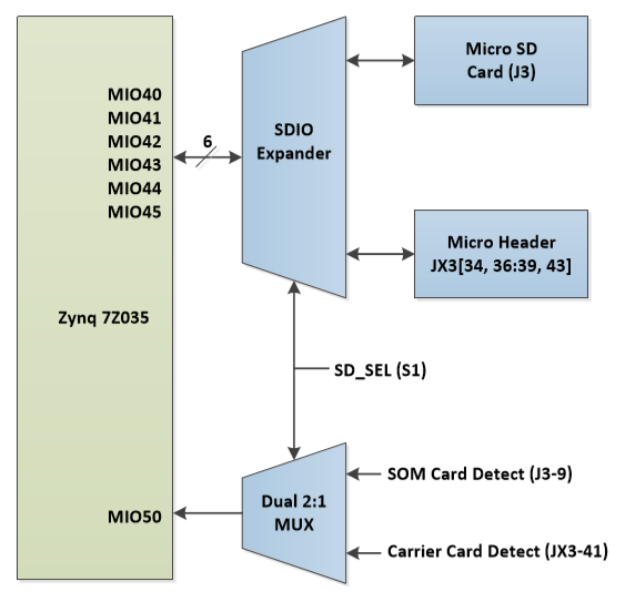
For example, the AD9361-Z7035 FMC Carrier implements a standard SD card interface as an alternative to using the micro SD card on the SOM. Switch S1 on the SOM selects the SD source connected to Zynq, as explained below.
Signal |
Description |
Zynq pin |
|---|---|---|
SD_SEL |
SOM Switch S1 (SD Card Select) |
0 = SOM micro SD; 1 = Carrier SD; (White dot on switch is logic 0.) |
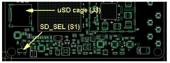 Micro SD Cage and Select Switch
The Zynq PS peripheral sd0 is connected through Bank 1/501 MIO[40-45]. The Card Detect signals from the SOM (J3-9) and carrier (JX3_SD1_CDN) are multiplexed on the SOM with the ADG772 dual 2:1 MUX (U5), onto one signal connected to Zynq PS MIO50.
Signal Name |
Description |
Zynq pin |
MIO |
2nd SD Channel on JX3 |
|---|---|---|---|---|
SD0_CLK |
Clock |
C22 (MIO Bank 1/501) |
40 |
JX3-43 |
SD0_CMD |
Command |
C19 (MIO Bank 1/501) |
41 |
JX3-34 |
SD0_DATA0 |
Data[0] |
F17 (MIO Bank 1/501 ) |
42 |
JX3-37 |
SD0_DATA1 |
Data[1] |
D18 (MIO Bank 1/501) |
43 |
JX3-36 |
SD0_DATA2 |
Data[2] |
E18 (MIO Bank 1/501) |
44 |
JX3-39 |
SD0_DATA3 |
Data[3] |
C18 (MIO Bank 1/501) |
45 |
JX3-38 |
PS_MIO50_501_SD0_CD |
Shared Card Detect signal |
B22 (MIO Bank 1/501) |
50 |
JX3-41 |
Zynq PS SDIO Connections
The micro SD Card is a 3.3V interface but is connected through MIO Bank 1/501 which is set to 1.8V. Therefore, the SDIO expander device performs voltage translation. As stated in the Zynq Technical Reference Manual (TRM), host mode is the only mode supported configuration.
The micro SD Card connector is located at J3 on the SOM. If you are using the SD Card for a file system a Class 10 card or better is recommended. We use SanDisk and Delkin. Other vendor cards may work as well, however we’ve experienced issues with a few brands.
USB 2.0 OTG
The Zynq Z-7035 PS contains two hardened USB 2.0 high speed controllers with on-the-go (OTG) dual role USB host controller or USB device controller operation using the same hardware. AD9361-Z7035 uses one of these Zynq PS peripherals, in combination with a USB2.0 UTMI+ low pin interface (ULPI) PHY device, to provide USB 2.0 OTG signaling to the JX3 connector.
The external Microchip USB3320 PHY presents an 8-bit ULPI interface to the Zynq PS MIO[28:39] pins in Bank 1/501, corresponding to the Zynq PS USB0 peripheral. The USB PHY Reset signal is connected to Zynq PS MIO[7] Bank 0/500. Signal PS_MIO7 is a 1.8V signal with a pull-up resistor which instructs VMODE[0] to set MIO[0:15] to LVCMOS18 signal standard up boot time.
The USB3320 PHY features a complete HS-USB Physical Front-End supporting speeds of up to 480Mbs. VDDIO for this device can be 1.8V or 3.3V, and on the AD9361-Z7035 it is powered at 1.8V. The PHY is connected to MIO Bank 1/501, which is also powered at 1.8V. This is critical since a level translator cannot be used as it would impact the tight ULPI timing required between the PHY and the Zynq device.
Additionally, the USB PHY must clock the ULPI interface which requires a 24 MHz crystal or oscillator (configured as ULPI Output Clock Mode). On the AD9361-Z7035 module, the 24 MHz oscillator is an Abracon ASDMB CMOS oscillator. The oscillator may be powered down using the STANDBY pin, which is controlled by the Zynq PS MIO[9] pin in Bank1/500.
The AD9361-Z7035 module does not include the USB connector. The SOM is designed to have the USB connector reside on the mating carrier card. The four USB connector signals (USB_OTG_P, USB_OTG_N, USB_ID, and USB_OTG_CPEN) are connected to the JX3 micro header receptacle. The table below shows the connections of these four signals at JX3.
Signal Name |
JX3 Pin |
|---|---|
USB_OTG_N |
69 |
USB_OTG_P |
67 |
USB_ID |
63 |
USB_OTG_CPEN |
70 |
USB 2.0 JX3 Pin Assignments
The AD9361-Z7035 module is configured such that either Host Mode (OTG) or Device Mode can be used depending on the circuitry of the carrier card. With a standard connection to a baseboard (no power supply used to provide USB power to the connector), the device will operate in Device Mode. Using the USB_OTG_CPEN signal on JX3 allows you to control an external power source for USB VBUS on the carrier board. Other considerations need to be made to accommodate Host Mode.
Signal Name |
Description |
Zynq Bank |
MIO |
SSMC3320 Pin |
SOM JX3 pins |
|---|---|---|---|---|---|
Data[7:0] |
USB Data Lines |
(MIO Bank 1/501) |
28:39 |
Data[7:0] |
N/A |
REFCLOCK |
USB Clock |
(MIO Bank 1/501) |
28:39 |
26 |
N/A |
DIR |
ULPI DIR output signal |
(MIO Bank 1/501 ) |
28:39 |
31 |
N/A |
STP |
ULPI STP input signal |
(MIO Bank 1/501) |
28:39 |
29 |
N/A |
NXT |
ULPI NXT output signal |
(MIO Bank 1/501) |
28:39 |
2 |
N/A |
REFSEL[2:0] |
USB Chip Select |
NC |
NC |
8,11,14 |
N/A |
DP |
DP pin of USB connector |
NC |
NC |
18 |
67 |
DM |
DM pin of USB connector |
NC |
NC |
19 |
69 |
ID |
Identification pin of the USB connector |
NC |
NC |
23 |
63 |
CPEN |
5V external Vbus power switch |
NC |
NC |
17 |
70 |
RESET_B |
Reset |
(MIO Bank 0/500) |
7 |
27 |
N/A |
USB Host Pin Assignment and Definitions
10/100/1000 Ethernet PHY
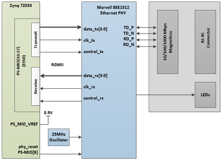
The Zynq PS includes two 10/100/1000 hardened Ethernet MAC ports. AD9361-Z7035 implements one Zynq PS 10/100/1000 Ethernet port (Eth0) for network connection using a Marvell 88E1512 PHY. A unique MACID for this port is provided with each SOM as a printed label on the module. It must be manually entered in Linux or included in the boot files for Zynq. A second Ethernet interface can be implemented by using the spare user I/O available on AD9361-Z7035.
The Marvell PHY operates at 1.8V. The PHY connects to Zynq PS MIO Bank 1/501 (1.8V) with an RGMII interface. The PHY reset connects to Zynq PS MIO[8] Bank 0/500.
The AD9361-Z7035 module does not include the RJ-45 interface. The signals are connected to the JX3 micro header receptacle. The intent is that the magnetics and RJ-45 jack are located on the carrier card. An example design enabling two Ethernet ports with RJ-45 connectors can be found in the AD9361-Z7035 FMC Carrier Card.
10/100/1000 Ethernet Interface
Zynq requires a voltage reference for RGMII interfaces. Thus PS_MIO_VREF, Zynq pin H18, is tied to 0.9V, half the bank voltage of MIO Bank 1/501. The 0.9V reference is generated through a resistor divide circuit. The 88E1512 also requires a 25 MHz input clock. A FOX ABM8G25.000MHZ-18-D2Y-T crystal is used as this reference.
Signal Name |
Description |
Zynq Pin |
MIO |
Zynq Bank |
88E1512 pin |
|---|---|---|---|---|---|
RX_CLK |
Receive Clock |
G22 |
16:27 |
1 / 501 |
46 |
RX_CTRL |
Receive Control |
F18 |
16:27 |
1 / 501 |
43 |
RXD[3:0] |
Receive Data |
RXD0: F20 RXD1: J19 RXD2: F19 RXD3: H17 |
16:27 |
1 / 501 |
44 45 47 48 |
TX_CLK |
Transmit Clock |
G21 |
16:27 |
1 / 501 |
53 |
TX_CTRL |
Transmit Control |
F22 |
16:27 |
1 / 501 |
56 |
TXD[3:0] |
Transmit Data |
TXD0: G17 TXD1: G20 TXD2: G19 TXD3: H19 |
16:27 |
1 / 501 |
50 51 54 55 |
MDIO |
Management Data |
A19 |
53 |
1 / 501 |
8 |
MDC |
Management Clock |
A20 |
52 |
1 / 501 |
7 |
ETH_RST_N |
PHY Reset |
A24 |
47 |
0 / 500 |
16 |
Zynq PS Ethernet PHY Pin Assignment and Definitions
Note: The datasheet for the Marvell 88E1512 is not available publicly. An NDA is required for this information. Contact your local Marvell representative for assistance.
User I/O
This section describes the various I/O available for use on the AD9361-Z7035 2X2 SOM. Pin out details of the available I/O are included later in the Expansion Headers section.
AD9361-Z7035 2X2 SOM features four 100-pin micro header receptacles (FCI, 61082-103400LF) for compact connection to carrier cards. The connector makes available 193 Zynq PL user SelectIO pins, 12 Zynq PS MIO pins, and 4 AD9361 GPO pins - a total of 209 available user I/O. In addition, four Zynq GTX gigabit serial transceiver ports are brought to the micro headers, each comprised of one TX and one RX lane and capable of speeds up to 6.6Gbps. Inputs for two GTX reference clocks are also available at the micro header. Finally, auxiliary data converters provide analog signal interface outside of the AD9361 primary RF path, as described later in the ‘User Auxiliary ADC and DAC Interfaces’ section.
AD9361 User Pins
AD9361-Z7035 2X2 provides access to four general purpose output pins GPO[3:0] from the AD9361. These pins are normally controlled by the AD9361 state machine, and can be linked to the TDD block (for controlling external Tx/Rx switches), or the AD9361 automatic gain control (ACG) block (for external LNA control), or optionally by registers, accessed through an SPI interface between the Zynq SoC and the AD9361.
The four AD9361 GPO signals are output only. The AD9361-Z7035 SOM sets the VDDA_GPO voltage level for these pins at 2.5V, but this can be overridden (voltage can be increased up to 3.3V) by placing a higher voltage on the VDDA_GPO_PWR pin on JX4.9
Zynq PS MIO User Pins
The Zynq Z-7035 SoC has 54 PS-MIO pins that connect to the Zynq Processor Sub-System (PS). AD9361-Z7035 makes 12 of these pins available as general purpose I/O while the remaining 42 are dedicated to peripheral and memory interfaces. Table 8 summarizes these signals.
The 12 available MIO pins can be used to implement of a variety of digital peripherals such as SPI, SDIO, CAN, UART, and I2C. These I/O pins can also be used as general purpose IO to connect push buttons, LEDs, and/or switches to the Zynq from the carrier card.
Note: The PS MIO banks are powered at 1.8V.
Signal Name |
MIO Signals |
Bank |
Bank Voltage |
Available Pins |
|---|---|---|---|---|
Available User MIO |
0,10-15 |
500 |
1.8V |
7 |
46-49, 51 |
501 |
1.8V |
5 |
|
Total |
12 |
|||
Interface |
MIO Signals |
Bank |
Bank Voltage |
Dedicated Pins |
QSPI_0 FLASH |
1-6, 8 |
500 |
1.8V |
7 |
USB_0 |
7, 28-39 |
500/501 |
1.8V |
13 |
Ethernet_0 |
16-27, 47, 52-53 |
500/501 |
1.8V |
15 |
SDIO_0 |
40-45, 50 |
501 |
1.8V |
7 |
Total |
42 |
Zynq PS MIO Bank Summary
Zynq PL SelectIO User Pins
AD9361-Z7035 provides 193 user SelectIO pins which connect to the Zynq Programmable Logic (PL). The voltage for these PL user I/O are set by the carrier card; supplied to the SOM through the JX micro header receptacles. This creates a highly flexible architecture for custom user functions and interfaces implemented in the Zynq Programmable Logic.
All Zynq SelectIO pins can be configured as either Input or Output with voltage signaling standards compliant with their bank voltage. The bank voltages must be delivered by the mating carrier card and within the ranges specified in the table below. Consult the Xilinx 7 Series FPGAs SelectIO Resources User Guide UG471) for information about supported I/O signaling standards.
The PL I/O pins are routed with matched lengths to each of the JX connectors. The matched pairs, denoted by an N/P suffix (e.g. IO_L01_13_JX2_P, IO_L01_13_JX2_N) may be used as either single ended I/O or differential pairs depending on the end user’s design requirements.
Differential LVDS pairs on a -2L speed grade device are capable of DDR data rates up to 1250Mbps for High Range (HR) banks and 1400 Mbps for High Performance (HP) banks. Additionally, eight of these I/O can be connected as clock inputs (i.e., four MRCC and four SRCC inputs). Each Zynq PL bank can also be configured to be a memory interface with up to four dedicated DQS data strobes and data byte groups. One of the differential pairs (IO_L03_34_JX4_P) in Zynq Bank 34 (Zynq pin H9) is shared with the Zynq “PUDC_B” signal.
Bank |
Bank Voltage |
Type |
Available Pins |
Available as LVDS Pairs |
Max DDR LVDS Rate |
|---|---|---|---|---|---|
12 |
Set by carrier (1.2 - 3.3V) |
HR |
50 |
24 |
1250 Mbps |
13 |
Set by carrier (1.2 - 3.3V) |
HR |
48 |
23 |
1250 Mbps |
33 |
Set by carrier (1.2 - 1.8V) |
HP |
50 |
24 |
1400 Mbps |
34 |
Set by carrier (1.2 - 1.8V) |
HP |
45 |
22 |
1400 Mbps |
Total |
193 |
94 |
Zynq PL User I/O Bank Summary
A detailed mapping of user I/O to the SOM micro header receptacle pins can be found in the Expansion Headers section.
When using the PL I/O pins care must be taken to ensure that any external signal interface adheres to the respective Zynq PL bank voltages. The carrier card provides the I/O VCCO voltages for the banks shown in Table 9. Therefore a custom carrier card can support mixed I/O voltage interfaces to the Zynq PL.
Note: The following are restrictions of the AD9361-Z7035 Zynq Z-7035 SelectIO banks:
Banks 33 and 34 are high performance (HP) I/O with support for I/O voltage from 1.2 to 1.8V.
Banks 12 and 13 are high range (HR) I/O with support for I/O voltage from 1.2V to 3.3V and Digitally Controlled Impedance (DCI).
All 4 banks support LVDS.
Consult the Xilinx 7 Series FPGAs SelectIO Resources User Guide UG471 for more information.
It is recommended any custom interface is run through the Xilinx Vivado™ tool suite for a design rule check on place and route and timing closure in advance of end user carrier card manufacturing.
User Auxiliary ADC and DAC Interfaces
In addition to the data converters included inside of the AD9361 primary signal chain, AD9361-Z7035 provides access to auxiliary data converters in the AD9361 and Zynq SoC.
AD9361 Auxiliary ADC
The AD9361 contains an auxiliary ADC that can be used to monitor system functions such as temperature or power output. The converter is 12 bits wide and has an input range of 0.05 V to 1.25 V. When enabled, the ADC is free running. SPI reads provide the last value latched at the ADC output. A multiplexer in front of the ADC allows you to select between the AUXADC input pin and a built-in temperature sensor. Both the Linux IIO device driver for the AD9361 and the no-OS driver for the AD9361 expose the built-in temperature sensor and external ADC channel with easy to use entries in sysfs or standard APIs.
AD9361-Z7035 wires the AD9361 single-ended AUXADC pin to the JX micro header receptacle JX4-7.
AD9361 Auxiliary DACs
The AD9361contains two identical auxiliary DACs that can provide power amplifier (PA) bias or other system functionality. The auxiliary DACs are 10 bits wide, have an output voltage range of 0.5 V to VDD_GPO − 0.3 V, a current drive of 10 mA, and can be directly controlled by the internal enable state machine.
AD9361-Z7035 wires the AD9361 single-ended AUXDAC1 and AUXDAC2 pins to the JX micro header receptacle JX4-8 and JX4-10 respectively.
More information on the AD9361 auxiliary data converters can be found here.
Zynq SoC ADC
The Zynq SoC includes the Xilinx Analog-to-Digital Converter (XADC) which contains two 12-bit 1MSPS ADCs with separate track and hold amplifiers, an on-chip analog multiplexer (up to 17 external analog input channels supported), and on-chip thermal and supply sensors. The two ADCs can be configured to simultaneously sample two external-input analog channels. The track and hold amplifiers support a range of analog input signal types, including unipolar, bipolar, and differential. The analog inputs can support signal bandwidths of at least 500 KHz at sample rates of 1MSPS. More information on the XADC can be found in Xilinx document UG480.
AD9361-Z7035 provides access to the primary XADC differential analog input on Zynq pins VP_0/VN_0, sampled by Zynq ADC_A. The differential pins are wired to AD9361-Z7035 JX micro header receptacle pins JX3-1 (V_0_P) and JX3-3 (V_0_N).
A Zynq internal multiplexer allows sampling of the following:
External analog signals at VP_0/VN_0 pins
Internal die temp sensor
External thermal diode connected to DXP_0/DXN_0 (SOM pin JX1-98, JX1-100)
Zynq Multi-Gigabit Transceivers (MGTs)
AD9361-Z7035 2X2 enables four of the eight gigabit full-duplex GTX transceiver lanes that reside on Bank 111 (SOM Rev A-C) or Bank 112 (SOM Rev D and beyond) of the Zynq XC7Z035-L2 FBG676I device. These high speed transceivers can be used to interface to multiple high speed interface protocols such as PCI Express, Ethernet, Serial ATA, and more.
The Xilinx XC7Z035-L2 FBG676I is enabled with GTX transceivers which are capable of a transceiver data rate up to 6.6 Gb/s.
Two differential MGT reference clock inputs are available for use with the GTX lanes. Either clock input can be used as the clock reference for any one of the GT lanes in the bank. This allows you to implement various protocols requiring different line rates. The SOM implements dc-blocking capacitors in series with these GTX reference clocks, but not on the data signals.
Gigabit transceiver lanes and their associated reference clocks are connected to the carrier board via the JX micro header receptacles. The table below shows the connections between the Zynq device and the JX micro header. Pin assignments can be found later on in a pair of large tables.
Performance of the four GTX lanes implemented on AD9361-Z7035 was validated to run at the rated maximum rate of 6.6GB/s. Tests were performed by using the Xilinx Vivado™ serial I/O analyzer software with the Xilinx LogiCORE™ IP Integrated Bit Error Ratio Test (IBERT) core for 7 series FPGA GTX transceivers.
GTX |
JX Connector |
|---|---|
MGTREFCLK0_N/P |
JX1 |
MGTXRX [3:1] _N/P |
JX1 |
MGTXTX [3:1] _N/P |
JX3 |
MGTREFCLK1_N/P |
JX3 |
Clock sources
High performance RF designs require knowledge of the digital clocks in the system because they can impart unwanted spurs into the RF signal chain. This section details the clocks used on the AD9361-Z7035 2X2 SOM and indicates which can be disabled in case of undesired spurs or to implement the lowest power design.
Zynq clocks
AD9361-Z7035 2X2 connects a dedicated 33.3333 MHz clock source to the Zynq SoC Processor Subsystem (PS). An ABRACON ASDMB-33.333MHZ-LC-T with 40-ohm series termination is used. The Zynq PS infrastructure can generate up to four PLL-based clocks for the Zynq Programmable Logic (PL) system. The Zynq Z-7035 PL has eight clock management tiles (CMTs), each consisting of one mixed-mode clock manager (MMCM) and one phase-locked loop (PLL).
AD9361 clocks
The AD9361 operates using a reference clock that can be provided by two different sources. This reference clock is used to supply the synthesizer blocks that generate all data clocks, sample clocks, and local oscillators inside the device.
AD9361-Z7035 provides an on-board 40MHz crystal and an external clocking option by using an analog multiplexor (ADG772). The on-board 40MHz crystal is from Rakon (MFR part # 513371). If an external oscillator is used, the frequency can vary between 10 MHz and 80 MHz. The selection between the two clock sources is under control of a Zynq PL pin in Bank 34 (K11).
The ability to use an external clock source for the AD9361 enables multi-SOM synchronization when used in conjunction with the SYNC_IN signal connected to the Zynq SoC.
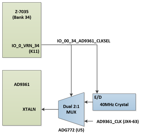
In addition to these clocks, the AD9361 creates an output data clock for the Zynq PL.
AD9361/Zynq SoC Connection.
Ethernet Clock
The Marvell 88E1512 Ethernet PHY onboard AD9361-Z7035 2X2 receives a 25 MHz input reference clock from a FOX ABM8G-25.000MHZ-18-D2Y-T crystal. This reference cannot be disabled.
The PHY RX_CLK may be disabled through the MDIO management interface. The PHY TX_CLK is supplied by the Zynq PS Ethernet controller and may be disabled in software.
USB Clock
AD9361-Z7035 2X2 uses the Microchip USB3320 Transceiver. The device receives a 24.00MHz clock from a CMOS oscillator which may be powered down with the PS_MIO09_500_USB_CLK_PD signal, controlled by software on the Zynq PS.
The USB3320 transceiver uses an internal PLL to generate a 60MHz clock for the ULPI interface to Zynq. If the 24MHz reference clock is stopped while 60MHz CLKOUT is running, the PLL will come out of lock and the frequency of the CLKOUT signal will decrease to the minimum allowed by the PLL design. This may cause the USB session to drop. Alternatively, the link controller (Zynq PS) can send a command to enter low power mode thereby disabling the USB3320 60MHz CLKOUT signal. 3.10.5 SDIO Clock The Zynq SoC provides an SDIO clock for the SD card interface. The SDIO clock frequency and output buffer can be controlled by software using the Zynq PS MIO registers. Consult the Xilinx Zynq-7000 Technical Resource Manual (UG585) for more information.
Reset Sources
AD9361 Reset
The AD9361 has a single asynchronous reset pin (RESETB) that is connected directly to the Zynq SoC on Bank 35 - pin H16. Asserting this signal to logic low resets the device and triggers the automatic initialization calibrations. This is managed by the AD9361 device driver, and should not be managed by the end user.
Zynq Power‐on Reset (PS_POR_B)
The Zynq PS supports an external power-on reset signal. The power-on reset is the master reset of the entire chip. This signal resets every register in the device capable of being reset. On AD9361-Z7035, this pin is connected to the power-good output of the final stage of the power regulation circuitry (PWR_GD_1.35V) which holds the Zynq PS_POR_B signal low until the output voltage is valid. In addition, a push button switch (SW1) is connected to PS_POR_B and GND to allow a manual hard reset of the Zynq device.
Zynq PROGRAM_B, DONE, PUDC_B, INIT_B Pins
The Zynq SoC includes several signals related to power up, programming, and reset. This section explains how these signals have been implemented on AD9361-Z7035 2X2. Consult Xilinx UG585 for an explanation of these signals.
Zynq Signal |
Description |
SOM |
User Access |
|---|---|---|---|
INIT_B |
Zynq open-drain I/O used to indicate when the PL is initializing or when a configuration error has occurred |
Wired to 3.3V with a 4.7kΩ resistor and accessible as a user signal. |
JX2-9 |
Program_B |
Zynq input used to reset the PL |
Wired to 3.3V with a 4.7kΩ resistor and not accessible as a user signal |
NA |
Done |
Zynq drives the DONE signal Low until the PL is configured |
Wired to a green LED (D4) turns OFF when the PL is configured. DO NOT LOAD SIGNAL |
JX1-8 |
PUDC_B |
Zynq pin controls the state of all Zynq PL SelectIO pins during power up |
1kΩ pull-down resistor and the accessible as user I/O. During power up and configuration the Zynq PL SelectIO pins will have internal pull-up resistors enabled until the device comes out of power-on reset (POR) |
JX4-25 |
Zynq Power Up / Reset Signals
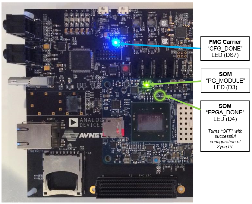
The Zynq SoC provides a DONE signal to indicate when the PL has been programmed. AD9361-Z7035 2X2 uses this signal to control an LED on the SOM. The green LED D4 turns on when the SOM is powered and turns off when the Zynq PL is configured. The signal is routed to the micro header receptacle JX1-8 (FPGA_DONE) for connection to the carrier card if needed for any additional startup logic.
Important
Do not load the FPGA_DONE signal on your carrier. It is sampled internally by the Zynq device. Loading the signal may delay the signal rise/fall times and cause errors during startup.
When mating the SOM to the AD9361-Z7035 FMC Carrier Card, a blue LED labeled “CFG DONE” will illuminate when configuration is complete.
 System Ready LEDs
Zynq Processor Subsystem Reset
System reset, labeled PS_SRST_B, resets the processor as well as erases all debug configurations. This external system reset allows you to reset all the functional logic within the device without disturbing the debug environment. For example, the previous break points you set remain valid after system reset. While PS_SRST_B is held Low, all PS I/Os are held in 3-state.
Due to security concerns, system reset erases all memory content within the PS, including the OCM. The PL is also reset in system reset. System reset does not re-sample the boot mode strapping pins.
This active-low signal can be asserted via the carrier card through the micro header interface at JX1-6. If it is not used on a carrier card, this signal should be tied high.
Note: This signal cannot be asserted while the boot ROM is executing following a POR reset. If PS_SRST_B is asserted while the boot ROM is running through a POR reset sequence it will trigger a lock-down event preventing the boot ROM from completing. To recover from lockdown the device either needs to be power cycled or PS_POR_B needs to be asserted.
Configuration Modes
The Zynq-7000 AP SoC has seven boot mode strapping pins that are hardware programmed on the SOM using MIO pins [8:2]. They are sampled by the hardware soon after PS_POR_B deasserts and their values are written to software readable registers for use by the Boot ROM and user software.
Zynq-7000 AP SoC devices use a multi-stage boot process that supports both non-secure and secure boot. The Zynq PS is the master of the boot and configuration process. Upon reset, MIO[5:3] pins are read to determine the primary boot device to be used: NOR, NAND, Quad-SPI, SD Card, or JTAG. AD9361-Z7035 2X2 enables three of those boot devices: QSPI, SD Card, and JTAG. The SOM contains switches to easily switch settings.
The Zynq PS SD/SDIO peripheral is connected to an SDIO expander chip (U11), providing connectivity to the micro SD interface on the AD9361-Z7035 SOM or a carrier card through the bottom-side micro header receptacle (JX3). Zynq can boot from either SD interface. The selection is made with switch S1 on the SOM. The table below shows the available boot mode configuration setting using switches S1, S3 and S4 on the SOM.
Boot Mode |
S4 (MIO4) |
S3 (MIO3) |
S1 |
|---|---|---|---|
CASCADE JTAG |
0 |
0 |
x |
NAND (n/a) |
0 |
1 |
x |
QSPI |
1 |
0 |
x |
SD Card (SOM) |
1 |
1 |
0 |
SD Card (Carrier) |
1 |
1 |
1 |
Note: White dot on switch is logic 0
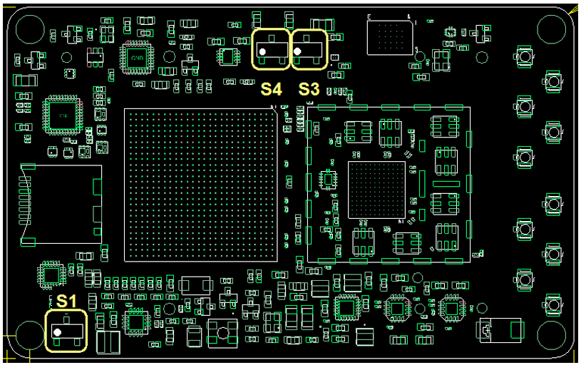 Zynq Boot Switches
AD9361-Z7035 powers the Zynq Bank 0 VCCO_0 at 3.3V. The configuration voltage select pin (CFGBVS) is pulled high with a 4.7KΩ resistor to set the JTAG I/O in Bank 0 for 3.3V/2.5V.
The Zynq PS is responsible for reconfiguring the PL. Zynq will not automatically reconfigure the PL as in standard FPGAs by toggling PROG. Likewise, it is not possible to hold off Zynq boot up with INIT_B as this is now done with POR. If the application needs to reconfigure the PL, the software design must do this, or you can toggle PS_POR_B to restart everything.
JTAG Connections
AD9361-Z7035 2X2 requires an external JTAG cable connector populated on the carrier card for JTAG operations. JTAG signals are routed from Bank 0 of the Zynq to the micro header receptacle JX1. The table below shows the JTAG signal connections between the Zynq and the micro header receptacle.
The Zynq Bank 0 reference voltage, Vcco_0, is connected to 3.3V. The JTAG Vref on the End User Carrier Card should be connected to 3.3V to ensure compatibility between the interfaces. For reference, see the AD9361-Z7035 FMC Carrier Card schematics.
SoC Pin# |
ADRV9361-Z7035 Net |
JX1 Pin # |
|---|---|---|
W12 |
JTAG_TCK |
1 |
W11 |
JTAG_TMS |
2 |
W10 |
JTAG_TDO |
3 |
V11 |
JTAG_TDI |
4 |
JTAG Pin Connections
RF Connections
The AD9361-Z7035 SOM connects four RX and four TX analog RF channels to the AD9361, plus two TX Monitor inputs. The TX/RX analog RF signals have series RF differential-to-single ended transformers from Mini Circuits (TCM1-63AX+). These are 50Ω transformers featuring a wideband frequency range of 10MHz to 6.0GHz, enabling the full supported bandwidth of the AD9361. The single-ended signals are connected to U.FL miniature coaxial connectors. This creates a compact interface to external modules for amplification and antennae mating on a carrier card.
Important
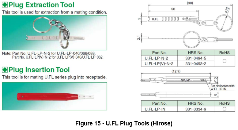
Take care when plugging and unplugging cables from the U.FL connectors to avoid damaging the surface mount connectors on the SOM. U.FL connectors were designed to connect to cables, not PCBs. It is not recommended to attempt a direct PCB-to-PCB mount with male connectors.
Plug insertion and extraction tools are recommended. An example from Hirose below. Details can be found in the Hirose catalog.
Sample transmit and receive circuits.
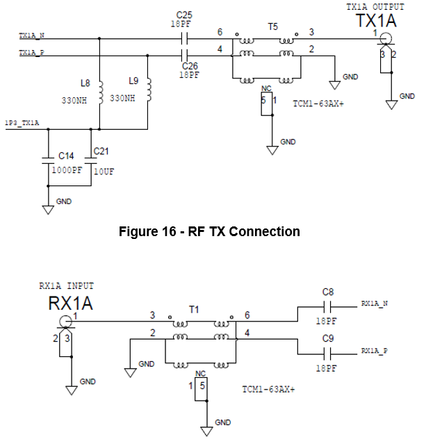
These are designed for wide band (70 MHz to 6 GHz) operation, and it is expected that a small external filter may be required to attenuate undesired signals.
Multi-SOM Synchronization
For MIMO systems requiring more than two input or two output channels, multiple AD9361-Z7035 modules and a common reference oscillator are required. The common reference oscillator can be provided from a customer carrier card. In addition, a logic pulse must be delivered to all AD9361 SYNC_IN inputs to align each device’s data clock with a common reference. On AD9361-Z7035, the SYNC_IN signal is connected directly to the Zynq PL. Again, a customer carrier card could route this signal to additional AD9361-Z7035 SOMs through any available user I/O.
To learn more about the AD9361 synchronization mechanism, consult the AD9361 Reference Manual.
Expansion Headers
Important
AD9361-Z7035 is not pin compatible with standard PicoZed (non-SDR) carrier cards.
The following tables summarize bank and signal assignments on the JX connectors. Detailed pin assignments are listed later in this section. Some of the connector pins are used for various power and ground assignments, and some pins are reserved for dedicated peripheral functions such as the Gigabit Ethernet, USB2.0 OTG, and SDIO ports of the AD9361-Z7035 SOM.
Micro Header Pin Summary
All Zynq PS-MIO and PL SelectIO pins can be configured as either Input or Output with voltage signaling standards compliant with their bank voltage. The bank voltages must be delivered by the mating carrier card and within the ranges specified in the following tables. Consult the Xilinx 7 Series FPGAs SelectIO Resources User Guide UG471 for information on supported I/O signaling standards.
The connectors are FCI 0.8mm Bergstak®, 100 Position, Dual Row, BTB Vertical Receptacles (part # 61082-103400LF). These have variable stack heights from 5mm to 16mm, making it easy to connect to a variety of carrier or system boards. Each pin can carry 500mA of current.
JX1 Pin Summary
Signals |
Source |
I/O Voltage |
Pins |
|---|---|---|---|
Bank 33 User I/O |
Zynq PL - Bank 33 (HP) |
Set by carrier 1.2V to 1.8V |
50 (24 LVDS pairs) |
MGTREFCLK0_P/N |
Zynq Bank 111/112(2) |
Set by carrier |
10 |
MGTRX_P/N[3:0] |
Zynq Bank 111/112(2) |
Set by carrier |
10 |
JTAG_TMS |
Zynq Bank 0 |
3.3V |
4 |
JTAG_TDI |
Zynq Bank 0 |
3.3V |
4 |
JTAG_TCK |
Zynq Bank 0 |
3.3V |
4 |
JTAG_TDO |
Zynq Bank 0 |
3.3V |
4 |
CARRIER_RESET (PS_SRST_B) |
Zynq Bank 501 |
1.8V |
1 |
FPGA_DONE |
Zynq Bank 0 |
3.3V |
1 |
FPGA_VBATT(1) |
Carrier |
See Zynq datasheet |
1 |
PWR_ENABLE |
Carrier |
5.0V max |
1 |
DXP_0 |
Zynq Bank 0 |
See Zynq datasheet |
2 |
DXN_0 |
Zynq Bank 0 |
See Zynq datasheet |
2 |
JX_VIN |
Carrier |
5.0V |
4 |
JX_VCCO_12 |
Carrier |
1.2 to 3.3V |
3 |
GND |
Carrier |
GND |
23 |
Total |
100 |
(1) FPGA_VBATT (VCCBATT) is required only when using bit-stream encryption. If battery is not used, connect VCCBATT to either ground or VCCAUX. (2) Rev C SOMs implement Zynq MGTs in Bank 111. Rev D and later SOMs use Bank 112.
JX2 Pin Summary
Signals |
Source I/O |
Voltage |
Pins |
|---|---|---|---|
Bank 12 User |
I/O Zynq PL - Bank 12 (HR) |
Set by carrier 1.2V to 3.3V |
14 (7 LVDS pairs) |
Bank 13 User |
I/O Zynq PL - Bank 13 (HR) |
Set by carrier 1.2V to 3.3V |
48 (23 LVDS pairs) |
SCL(1) |
Zynq PL - Bank 13 (HR) |
Set by carrier 1.2V to 3.3V |
2 |
SDA(1) |
Zynq PL - Bank 13 (HR) |
Set by carrier 1.2V to 3.3V |
2 |
INIT_B |
Zynq Bank 0 |
3.3V |
1 |
PG_MODULE |
SOM |
VIN |
1 |
PG_1P8V |
SOM |
1.8V |
1 |
JX_VIN |
Carrier |
5.0V |
5 |
JX_VCCO_13 |
Carrier |
1.2V to 3.3V |
1 |
JX_VCCO_33_34 |
Carrier |
1.2V to 1.8V |
3 |
GND |
Carrier |
GND |
23 |
Total |
99 |
(1) See Section 3.16.3 for information on using these I2C signals to program the SOM power sequencing devices.
JX3 Pin Summary
Signals |
Source |
I/O Voltage |
Pins |
|---|---|---|---|
Bank 12 User I/O |
Zynq PL - Bank 12 (HR) |
Set by carrier 1.2V to 3.3V |
32 (16 LVDS pairs) |
MGTREFCLK1_P/N |
Zynq Bank 111/112 (1) |
Set by carrier |
10 |
MGTTX_P/N[3:0] |
Zynq Bank 111/112 (1) |
Set by carrier |
10 |
V0_N/P |
Zynq Bank 0 |
See Zynq datasheet |
2 |
SDIO_DATA_B1 [3:0] |
Zynq PS - Bank 501 |
3.3V thru SDIO expander / translator |
6 |
SDIO_CLKB1 |
Zynq PS - Bank 501 |
3.3V thru SDIO expander / translator |
6 |
SDIO_CMDB1 |
Zynq PS - Bank 501 |
3.3V thru SDIO expander / translator |
6 |
JX3_SD1_CDN Zynq |
PS - Bank 501 |
1.8V thru Analog switch |
1 |
ETH_PHY_LED [1:0] |
Marvell 88E1512 PHY |
Open drain circuit |
2 |
ETHERNET MD [3:0] |
Zynq PS - Bank 501 (via Ethernet PHY) |
Set by SOM Ethernet PHY |
8 |
USB_OTG_P/N |
Zynq PS - Bank 501 (via USB PHY) |
Set by SOM USB PHY |
2 |
USB_ID |
Carrier |
0 to 3.3V |
3 |
USB_VBUS_OTG |
Carrier |
5.0V |
3 |
USB_OTG_CPEN |
SOM USB PHY |
3.3V |
3 |
JX_VCCO_13 |
Carrier |
1.2V to 3.3V |
2 |
JX_MGTAVCC |
Carrier |
1.05V |
4 |
JX_MGTAVTT |
Carrier |
1.2V |
2 |
GND |
Carrier |
GND |
26 |
Total |
100 |
(1) Rev C SOMs implement Zynq MGTs in Bank 111. Rev D and later SOMs use Bank 112.
JX4 Pin Summary
Signals |
Source |
I/O Voltage |
Pins |
|---|---|---|---|
Bank 12 User I/O |
Zynq PL - Bank 12 (HR) |
Set by carrier 1.2V to 3.3V |
4 (1 LVDS pair) |
Bank 34 User I/O |
Zynq PL - Bank 34 (HP) |
Set by carrier 1.2V to 1.8V |
44 (22 LVDS pairs) |
PUDC_B / User I/O (1) |
Zynq PL - Bank 34 (HP) |
Set by carrier 1.2V to 1.8V |
1 |
AD9361 GPO [3:0] |
AD9361 |
2.5V |
4 |
AD9361 AUXADC |
AD9361 |
See AD9361 datasheet |
3 |
AD9361 AUXDAC [1:0] |
AD9361 |
See AD9361 datasheet |
3 |
AD9361_CLK |
AD9361 |
1.3Vp-p |
1 |
PS_MIO [0,10:15] |
Zynq PS - Bank 500 |
1.8V |
7 |
PS_MIO [46:49, 51] |
Zynq PS - Bank 501 |
1.8V |
5 |
VDDA_GPO_PWR |
AD9361 |
2.5V |
1 |
GND |
Carrier |
GND |
28 |
Total |
98 |
(1) PUDC_B is a configuration pin for Zynq PL SelectIO during power on. The SOM implements a 1kΩ pulldown on this signal to enable internal pull-up resistors on each SelectIO pin. 3.15.2 Micro Header Pin Detail The section gives the detailed connection of all signals to the four micro header receptacle (JX) connector pins located on the bottom of the AD9361-Z7035 SOM. These connectors are used to connect the AD9361-Z7035 SOM to a carrier card. The carrier card powers the SOM and accesses all user I/O and dedicated peripherals through these micro headers located on the bottom of the SOM.
Important
AD9361-Z7035 is not pin compatible with standard PicoZed (non-SDR) carrier cards.
The AD9361-Z7035 product website has the following time saving resources.
SOM schematic symbol
Zynq master constraints file for Vivado Design Suite (XDC)
Important
The following tables are for reference. In case of discrepancies, use the software generated files listed above.
The signals names in the table below use the following nomenclature:
Zynq PL signals : IO_L##_<BANK#>_JX#_<N/P>
IO : Zynq Programmable Logic SelectIO input/output
L## : signal number within bank
BANK# : bank number
JX# : JX connector (1-4)
N/P : differential capable signal; otherwise single-ended
Zynq PS signals: PS_MIO##_<BANK #>_JX#
PS : Zynq Processor Subsystem input/output
MIO : Zynq PS MIO assignment
JX# : JX connector (1-4)
Other signals, such as USB_OTG_P, indicate connection to a dedicated peripheral interface on the SOM. In this case, a USB data signal that originates from the on-board USB2.0 PHY, which is controlled by the Zynq PS USB peripheral.
JX1 Connections
Zynq Bank |
Zynq Pin# |
AD9361-Z7035 Net |
JX1 Pin# |
JX1 Pin# |
AD9361-Z7035 Net |
Zynq Pin# |
Zynq Bank |
|---|---|---|---|---|---|---|---|
0 |
W12 |
JTAG_TCK |
1 |
2 |
JTAG_TMS |
W11 |
0 |
0 |
W10 |
JTAG_TDO |
3 |
4 |
JTAG_TDI |
V11 |
0 |
n/a |
n/a |
PWR_ENABLE(1) |
5 |
6 |
CARRIER_RESET(2) |
A22 |
501 |
0 |
V15 |
FPGA_VBATT |
7 |
8 |
FPGA_DONE |
W9 |
0 |
33 |
L9 |
IO_00_33_JX1 |
9 |
10 |
IO_25_33_JX1 |
N8 |
33 |
33 |
M2 |
IO_L16_33_JX1_P |
11 |
12 |
IO_L17_33_JX1_P |
N4 |
33 |
33 |
L2 |
IO_L16_33_JX1_N |
13 |
14 |
IO_L17_33_JX1_N |
M4 |
33 |
GND |
15 |
16 |
GND |
||||
33 |
N1 |
IO_L18_33_JX1_P |
17 |
18 |
IO_L19_33_JX1_P |
M7 |
33 |
33 |
M1 |
IO_L18_33_JX1_N |
19 |
20 |
IO_L19_33_JX1_N |
L7 |
33 |
GND |
21 |
22 |
GND |
||||
33 |
K5 |
IO_L20_33_JX1_P |
23 |
24 |
IO_L21_33_JX1_P |
M8 |
33 |
33 |
J5 |
IO_L20_33_JX1_N |
25 |
26 |
IO_L21_33_JX1_N |
L8 |
33 |
GND |
27 |
28 |
GND |
||||
33 |
K6 |
IO_L22_33_JX1_P |
29 |
30 |
IO_L23_33_JX1_P |
N7 |
33 |
33 |
J6 |
IO_L22_33_JX1_N |
31 |
32 |
IO_L23_33_JX1_N |
N6 |
33 |
GND |
33 |
34 |
GND |
||||
33 |
G4 |
IO_L01_33_JX1_P |
35 |
36 |
IO_L24_33_JX1_P |
K8 |
33 |
33 |
F4 |
IO_L01_33_JX1_N |
37 |
38 |
IO_L24_33_JX1_N |
K7 |
33 |
GND |
39 |
40 |
GND |
||||
33 |
D4 |
IO_L02_33_JX1_P |
41 |
42 |
IO_L03_33_JX1_P |
G2 |
33 |
33 |
D3 |
IO_L02_33_JX1_N |
43 |
44 |
IO_L03_33_JX1_N |
F2 |
33 |
GND |
45 |
46 |
GND |
||||
33 |
D1 |
IO_L04_33_JX1_P |
47 |
48 |
IO_L14_SRCC_33_JX1_P |
L5 |
33 |
33 |
C1 |
IO_L04_33_JX1_N |
49 |
50 |
IO_L14_SRCC_33_JX1_N |
L4 |
33 |
GND |
51 |
52 |
GND |
||||
33 |
N3 |
IO_L15_33_JX1_P |
53 |
54 |
IO_L05_33_JX1_P |
E2 |
33 |
33 |
N2 |
IO_L15_33_JX1_N |
55 |
56 |
IO_L05_33_JX1_N |
E1 |
33 |
n/a |
JX_VIN |
57 |
58 |
JX_VIN |
n/a |
||
n/a |
JX_VIN |
59 |
60 |
JX_VIN |
n/a |
||
33 |
F3 |
IO_L06_33_JX1_P |
61 |
62 |
IO_L07_33_JX1_P |
J1 |
33 |
33 |
E3 |
IO_L06_33_JX1_N |
63 |
64 |
IO_L07_33_JX1_N |
H1 |
33 |
GND |
65 |
66 |
GND |
||||
33 |
H4 |
IO_L08_33_JX1_P |
67 |
68 |
IO_L09_33_JX1_P |
K2 |
33 |
33 |
H3 |
IO_L08_33_JX1_N |
69 |
70 |
IO_L09_33_JX1_N |
K1 |
33 |
GND |
71 |
72 |
GND |
||||
33 |
H2 |
IO_L10_33_JX1_P |
73 |
74 |
IO_L11_SRCC_33_JX1_P |
L3 |
33 |
33 |
G1 |
IO_L10_33_JX1_N |
75 |
76 |
IO_L11_SRCC_33_JX1_N |
K3 |
33 |
GND |
77 |
78 |
JX_VCCO_12 |
n/a |
|||
n/a |
JX_VCCO_12 |
79 |
80 |
JX_VCCO_12 |
n/a |
||
33 |
J4 |
IO_L12_MRCC_33_JX1_P |
81 |
82 |
IO_L13_MRCC_33_JX1_P |
M6 |
33 |
J3 |
IO_L12_MRCC_33_JX1_N |
83 |
84 |
IO_L13_MRCC_33_JX1_N |
M5 |
33 |
|
GND |
85 |
86 |
GND |
||||
111 |
W6 |
MGTREFCLK0_111_JX1_P(3) |
87 |
88 |
MGTXRX0_111_JX1_P |
AD8 |
111 |
111 |
W5 |
MGTREFCLK0_111_JX1_N(3) |
89 |
90 |
MGTXRX0_111_JX1_N |
AD7 |
111 |
111 |
AE6 |
MGTXRX1_111_JX1_P |
91 |
92 |
MGTXRX2_111_JX1_P |
AC6 |
111 |
111 |
AE5 |
MGTXRX1_111_JX1_N |
93 |
94 |
MGTXRX2_111_JX1_N |
AC5 |
111 |
GND |
95 |
96 |
GND |
||||
111 |
AD4 |
MGTXRX3_111_JX1_P |
97 |
98 |
DX_0_P |
R14 |
0 |
111 |
AD3 |
MGTXRX3_111_JX1_N |
99 |
100 |
DX_0_N |
R13 |
0 |
(1) Has 10kΩ pull-up up resistor to VIN. (2) Connected to Zynq PS-SRST# signal through MOSFET switch enabled by VCCPCOM-1P8V. (3) Connected to Zynq pin with series dc-blocking capacitor.
JX2 Connections
Zynq Bank |
Zynq Pin# |
AD9361-Z7035 Net |
JX2 Pin# |
JX2 Pin# |
AD9361-Z7035 Net |
Zynq Pin# |
Zynq Bank |
|---|---|---|---|---|---|---|---|
13 |
AA25 |
IO_L01_13_JX2_P |
1 |
2 |
IO_L02_13_JX2_P |
AB26 |
13 |
13 |
AB25 |
IO_L01_13_JX2_N |
3 |
4 |
IO_L02_13_JX2_N |
AC26 |
13 |
13 |
AE25 |
IO_L03_13_JX2_P |
5 |
6 |
IO_L04_13_JX2_P |
AD25 |
13 |
13 |
AE26 |
IO_L03_13_JX2_N |
7 |
8 |
IO_L04_13_JX2_N |
AD26 |
13 |
0 |
INIT_B_0_JX2_09 |
9 |
10 |
PG_1P8V |
n/a |
n/a |
|
n/a |
n/a |
PG_MODULE(1) |
11 |
12 |
JX_VIN |
n/a |
|
13 |
V19 |
IO_00_13_JX2 |
13 |
14 |
IO_25_13_JX2 |
V18 |
13 |
GND |
15 |
16 |
GND |
||||
13 |
AF24 |
SCL |
17 |
18 |
IO_L06_13_JX2_P |
AA24 |
13 |
13 |
AF25 |
SDA |
19 |
20 |
IO_L06_13_JX2_N |
AB24 |
13 |
GND |
21 |
22 |
GND |
||||
13 |
AE22 |
IO_L07_13_JX2_P |
23 |
24 |
IO_L08_13_JX2_P |
AE23 |
13 |
13 |
AF22 |
IO_L07_13_JX2_N |
25 |
26 |
IO_L08_13_JX2_N |
AF23 |
13 |
GND |
27 |
28 |
GND |
||||
13 |
AB21 |
IO_L09_13_JX2_P |
29 |
30 |
IO_L10_13_JX2_P |
AA22 |
13 |
13 |
AB22 |
IO_L09_13_JX2_N |
31 |
32 |
IO_L10_13_JX2_N |
AA23 |
13 |
GND |
33 |
34 |
GND |
||||
13 |
AD23 |
IO_L11_SRCC_13_JX2_P |
35 |
36 |
IO_L12_MRCC_13_JX2_P |
AC23 |
13 |
13 |
AD24 |
IO_L11_SRCC_13_JX2_N |
37 |
38 |
IO_L12_MRCC_13_JX2_N |
AC24 |
13 |
GND |
39 |
40 |
GND |
||||
13 |
AD20 |
IO_L13_MRCC_13_JX2_P |
41 |
42 |
IO_L14_SRCC_13_JX2_P |
AC21 |
13 |
13 |
AD21 |
IO_L13_MRCC_13_JX2_N |
43 |
44 |
IO_L14_SRCC_13_JX2_N |
AC22 |
13 |
GND |
45 |
46 |
GND |
||||
13 |
AF19 |
IO_L15_13_JX2_P |
47 |
48 |
IO_L16_13_JX2_P |
AE20 |
13 |
13 |
AF20 |
IO_L15_13_JX2_N |
49 |
50 |
IO_L16_13_JX2_N |
AE21 |
13 |
GND |
51 |
52 |
GND |
||||
13 |
AD18 |
IO_L17_13_JX2_P |
53 |
54 |
IO_L18_13_JX2_P |
AE8 |
13 |
13 |
AD19 |
IO_L17_13_JX2_N |
55 |
56 |
IO_L18_13_JX2_N |
AF18 |
13 |
n/a |
JX_VIN |
57 |
58 |
JX_VIN |
n/a |
||
n/a |
JX_VIN |
59 |
60 |
JX_VIN |
n/a |
||
13 |
W20 |
IO_L19_13_JX2_N |
61 |
62 |
IO_L20_13_JX2_P |
AA20 |
13 |
13 |
Y20 |
IO_L19_13_JX2_P |
63 |
64 |
IO_L20_13_JX2_N |
AB20 |
13 |
GND |
65 |
66 |
GND |
||||
13 |
AC18 |
IO_L21_13_JX2_P |
67 |
68 |
IO_L22_13_JX2_P |
AA19 |
13 |
13 |
AC19 |
IO_L21_13_JX2_N |
69 |
70 |
IO_L22_13_JX2_N |
AB19 |
13 |
GND |
71 |
72 |
GND |
||||
13 |
W18 |
IO_L23_13_JX2_P |
73 |
74 |
IO_L24_13_JX2_P |
Y18 |
13 |
13 |
W19 |
IO_L23_13_JX2_N |
75 |
76 |
IO_L24_13_JX2_N |
AA18 |
13 |
GND |
77 |
78 |
JX_VCCO_33_34 |
n/a |
|||
n/a |
JX_VCCO_33_34 |
79 |
80 |
JX_VCCO_33_34 |
n/a |
||
12 |
AE17 |
IO_L18_12_JX2_P |
81 |
82 |
IO_L17_12_JX2_P |
AE16 |
12 |
12 |
AF17 |
IO_L18_12_JX2_N |
83 |
84 |
IO_L17_12_JX2_N |
AE15 |
12 |
GND |
85 |
86 |
GND |
||||
12 |
AB17 |
IO_L20_12_JX2_P |
87 |
88 |
IO_L19_12_JX2_P |
Y17 |
12 |
12 |
AB16 |
IO_L20_12_JX2_N |
89 |
90 |
IO_L19_12_JX2_N |
AA17 |
12 |
GND |
91 |
92 |
GND |
||||
12 |
AC17 |
IO_L21_12_JX2_P |
93 |
94 |
IO_L22_12_JX2_P |
AA15 |
12 |
12 |
AC16 |
IO_L21_12_JX2_N |
95 |
96 |
IO_L22_12_JX2_N |
AA14 |
12 |
12 |
Y16 |
IO_L23_12_JX2_P |
97 |
98 |
JX_VCCO_13 |
n/a |
|
12 |
Y15 |
IO_L23_12_JX2_N |
99 |
100 |
open |
Has 10kΩ pull-up up resistor to VIN.
JX 3 Connections
Zynq Bank |
Zynq Pin# |
AD9361-Z7035 Net |
JX3 Pin# |
JX3 Pin# |
AD9361-Z7035 Net |
Zynq Pin# |
Zynq Bank |
|---|---|---|---|---|---|---|---|
0 |
N14 |
V_0_P |
1 |
2 |
MGTREFCLK1_111_JX3_P(1) |
AA6 |
111 |
0 |
P13 |
V_0_N |
3 |
4 |
MGTREFCLK1_111_JX3_N(1) |
AA5 |
111 |
n/a |
JX_MGTAVCC |
5 |
6 |
GND |
|||
n/a |
JX_MGTAVCC |
7 |
8 |
MGTXTX0_111_JX3_P |
AF8 |
111 |
|
n/a |
JX_MGTAVCC |
9 |
10 |
MGTXTX0_111_JX3_N |
AF7 |
111 |
|
n/a |
JX_MGTAVCC |
11 |
12 |
GND |
|||
111 |
AF4 |
MGTXTX1_111_JX3_P |
13 |
14 |
MGTXTX2_111_JX3_P |
AE2 |
111 |
111 |
AF3 |
MGTXTX1_111_JX3_N |
15 |
16 |
MGTXTX2_111_JX3_N |
AE1 |
111 |
GND |
17 |
18 |
GND |
||||
111 |
AC2 |
MGTXTX3_111_JX3_P |
19 |
20 |
IO_L01_12_JX3_P |
Y12 |
12 |
111 |
AC1 |
MGTXTX3_111_JX3_N |
21 |
22 |
IO_L01_12_JX3_N |
Y11 |
12 |
GND |
23 |
24 |
GND |
||||
12 |
AB12 |
IO_L02_12_JX3_P |
25 |
26 |
IO_L03_12_JX3_P |
Y10 |
12 |
12 |
AC11 |
IO_L02_12_JX3_N |
27 |
28 |
IO_L03_12_JX3_N |
AA10 |
12 |
GND |
29 |
30 |
JX_MGTAVTT |
n/a |
|||
12 |
AB11 |
IO_L04_12_JX3_P |
31 |
32 |
JX_MGTAVTT |
n/a |
|
12 |
AB10 |
IO_L04_12_JX3_N |
33 |
34 |
SDIO_CMDB1 |
n/a |
n/a |
GND |
35 |
36 |
SDIO_DATB1 |
n/a |
n/a |
||
n/a |
n/a |
SDIO_DATB1 |
37 |
38 |
SDIO_DATB1 |
n/a |
n/a |
n/a |
n/a |
SDIO_DATB1 |
39 |
40 |
GND |
||
n/a |
n/a |
JX3_SD1_CDN |
41 |
42 |
IO_L05_12_JX3_P |
W13 |
12 |
n/a |
n/a |
SDIO_CLKB1 |
43 |
44 |
IO_L05_12_JX3_N |
Y13 |
12 |
n/a |
JX_VCCO_13 |
45 |
46 |
JX_VCCO_13 |
n/a |
||
n/a |
n/a |
ETH_PHY_LED0 |
47 |
48 |
ETH_PHY_LED1 |
n/a |
n/a |
GND |
49 |
50 |
GND |
||||
n/a |
n/a |
ETH_MD1_P |
51 |
52 |
ETH_MD2_P |
n/a |
n/a |
n/a |
n/a |
ETH_MD1_N |
53 |
54 |
ETH_MD2_N |
n/a |
n/a |
GND |
55 |
56 |
GND |
||||
n/a |
n/a |
ETH_MD3_P |
57 |
58 |
ETH_MD4_P |
n/a |
n/a |
n/a |
n/a |
ETH_MD3_N |
59 |
60 |
ETH_MD4_N |
n/a |
n/a |
GND |
61 |
62 |
GND |
||||
n/a |
n/a |
USB_ID |
63 |
64 |
IO_L06_12_JX3_P |
AA13 |
12 |
GND |
65 |
66 |
IO_L06_12_JX3_N |
AA12 |
12 |
||
n/a |
n/a |
USB_OTG_P |
67 |
68 |
USB_VBUS_OTG |
n/a |
n/a |
n/a |
n/a |
USB_OTG_N |
69 |
70 |
USB_OTG_CPEN |
n/a |
n/a |
GND |
71 |
72 |
GND |
||||
12 |
AE10 |
IO_L07_12_JX3_P |
73 |
74 |
IO_L08_12_JX3_P |
AE12 |
12 |
12 |
AD10 |
IO_L07_12_JX3_N |
75 |
76 |
IO_L08_12_JX3_N |
AF12 |
12 |
GND |
77 |
78 |
GND |
||||
12 |
AE11 |
IO_L09_12_JX3_P |
79 |
80 |
IO_L10_12_JX3_P |
AE13 |
12 |
12 |
AF10 |
IO_L09_12_JX3_N |
81 |
82 |
IO_L10_12_JX3_N |
AF13 |
12 |
GND |
83 |
84 |
GND |
||||
12 |
AC12 |
IO_L11_SRCC_12_JX3_P |
85 |
86 |
IO_L12_MRCC_12_JX3_P |
AC13 |
12 |
12 |
AD12 |
IO_L11_SRCC_12_JX3_N |
87 |
88 |
IO_L12_MRCC_12_JX3_N |
AD13 |
12 |
GND |
89 |
90 |
GND |
||||
12 |
AC14 |
IO_L13_MRCC_12_JX3_P |
91 |
92 |
IO_L14_SRCC_12_JX3_P |
AB15 |
12 |
12 |
AD14 |
IO_L13_MRCC_12_JX3_N |
93 |
94 |
IO_L14_SRCC_12_JX3_N |
AB14 |
12 |
GND |
95 |
96 |
GND |
||||
12 |
AD16 |
IO_L15_12_JX3_P |
97 |
98 |
IO_L16_12_JX3_P |
AF15 |
12 |
12 |
AD15 |
IO_L15_12_JX3_N |
99 |
100 |
IO_L16_12_JX3_N |
AF14 |
12 |
Connected to Zynq pin with series dc-blocking capacitor.
JX4 Connections
Zynq Bank |
Zynq Pin# |
AD9361-Z7035 Net |
JX4 Pin# |
JX4 Pin# |
AD9361-Z7035 Net |
Zynq Pin# |
Zynq Bank |
|---|---|---|---|---|---|---|---|
n/a |
n/a |
GPO_0 |
1 |
2 |
GPO_1 |
n/a |
n/a |
n/a |
n/a |
GPO_2 |
3 |
4 |
GPO_3 |
n/a |
n/a |
GND |
5 |
6 |
GND |
||||
n/a |
n/a |
AUXADC |
7 |
8 |
AUXDAC1 |
n/a |
n/a |
n/a |
n/a |
VDDA_GPO_PWR |
9 |
10 |
AUXDAC2 |
n/a |
n/a |
GND |
11 |
12 |
GND |
||||
12 |
W16 |
IO_L24_12_JX4_P |
13 |
14 |
IO_00_12_JX4 |
W14 |
12 |
12 |
W15 |
IO_L24_12_JX4_N |
15 |
16 |
IO_25_12_JX4 |
W17 |
12 |
GND |
17 |
18 |
GND |
||||
34 |
J11 |
IO_L01_34_JX4_P |
19 |
20 |
IO_L02_34_JX4_P |
G6 |
34 |
34 |
H11 |
IO_L01_34_JX4_N |
21 |
22 |
IO_L02_34_JX4_N |
G5 |
34 |
GND |
23 |
24 |
GND |
||||
34 |
H9 |
IO_L03_34_JX4_P(PUDC_B) |
25 |
26 |
IO_L04_34_JX4_P |
H7 |
34 |
34 |
G9 |
IO_L03_34_JX4_N |
27 |
28 |
IO_L04_34_JX4_N |
H6 |
34 |
GND |
29 |
30 |
GND |
||||
34 |
J10 |
IO_L05_34_JX4_P |
31 |
32 |
IO_L06_34_JX4_P |
J8 |
34 |
34 |
J9 |
IO_L05_34_JX4_N |
33 |
34 |
IO_L06_34_JX4_N |
H8 |
34 |
34 |
F5 |
IO_L07_34_JX4_P |
35 |
36 |
IO_L08_34_JX4_P |
D9 |
34 |
34 |
E5 |
IO_L07_34_JX4_N |
37 |
38 |
IO_L08_34_JX4_N |
D8 |
34 |
GND |
39 |
40 |
GND |
||||
34 |
F9 |
IO_L09_34_JX4_P |
41 |
42 |
IO_L10_34_JX4_P |
E6 |
34 |
34 |
E8 |
IO_L09_34_JX4_N |
43 |
44 |
IO_L10_34_JX4_N |
D5 |
34 |
34 |
F8 |
IO_L11_SRCC_34_JX4_P |
45 |
46 |
IO_L12_MRCC_34_JX4_P |
G7 |
34 |
34 |
E7 |
IO_L11_SRCC_34_JX4_N |
47 |
48 |
IO_L12_MRCC_34_JX4_N |
F7 |
34 |
GND |
49 |
50 |
GND |
||||
34 |
C8 |
IO_L13_MRCC_34_JX4_N |
51 |
52 |
IO_L14_SRCC_34_JX4_P |
D6 |
34 |
34 |
C7 |
IO_L13_MRCC_34_JX4_P |
53 |
54 |
IO_L14_SRCC_34_JX4_N |
C6 |
34 |
GND |
55 |
56 |
GND |
||||
34 |
C9 |
IO_L15_34_JX4_P |
57 |
58 |
IO_L16_34_JX4_P |
B10 |
34 |
34 |
B9 |
IO_L15_34_JX4_N |
59 |
60 |
IO_L16_34_JX4_N |
A10 |
34 |
GND |
61 |
62 |
GND |
||||
n/a |
n/a |
AD9361_CLK |
63 |
64 |
IO_25_34_JX4 |
K10 |
34 |
GND |
65 |
66 |
GND |
||||
34 |
A9 |
IO_L17_34_JX4_P |
67 |
68 |
IO_L18_34_JX4_P |
B7 |
34 |
34 |
A8 |
IO_L17_34_JX4_N |
69 |
70 |
IO_L18_34_JX4_N |
A7 |
34 |
GND |
71 |
72 |
GND |
||||
34 |
C4 |
IO_L19_34_JX4_P |
73 |
74 |
IO_L20_34_JX4_P |
B5 |
34 |
34 |
C3 |
IO_L19_34_JX4_N |
75 |
76 |
IO_L20_34_JX4_N |
B4 |
34 |
34 |
B6 |
IO_L21_34_JX4_P |
77 |
78 |
IO_L22_34_JX4_P |
A4 |
34 |
34 |
A5 |
IO_L21_34_JX4_N |
79 |
80 |
IO_L22_34_JX4_N |
A3 |
34 |
n/a |
n/a |
3V3_I2C |
81 |
82 |
open |
||
GND |
83 |
84 |
GND |
||||
500 |
C24 |
PS_MIO15_500_JX4 |
85 |
86 |
PS_MIO12_500_JX4 |
A23 |
500 |
500 |
A25 |
PS_MIO10_500_JX4 |
87 |
88 |
PS_MIO11_500_JX4 |
B26 |
500 |
GND |
89 |
90 |
GND |
||||
500 |
B25 |
PS_MIO13_500_JX4 |
91 |
92 |
PS_MIO46_501_JX4 |
E17 |
501 |
500 |
D23 |
PS_MIO14_500_JX4 |
93 |
94 |
PS_MIO47_501_JX4 |
B19 |
501 |
GND |
95 |
96 |
GND |
||||
500 |
E26 |
PS_MIO00_500_JX4 |
97 |
98 |
PS_MIO49_501_JX4 |
A18 |
501 |
501 |
B21 |
PS_MIO48_501_JX4 |
99 |
100 |
PS_MIO51_501_JX4 |
B20 |
501 |
(1) On AD9361-Z7035, the PUDC_B signal has a 1kΩ pull-down resistor. Therefore, during power-up and configuration the Zynq PL SelectIO pins will have internal pull-up resistors enabled until the device comes out of power-on reset (POR).
Power
The AD9361-Z7035 2X2 SOM was designed to reduce power consumption at every angle. The major features of the power system are as follows:
The -2LI Xilinx Z-7035 is a low-power, mid-speed grade device that offers 40% lower static power and 10% lower dynamic power than a standard -2I device.
Low power DDR3L Micron SDRAM provides 15% or more power savings over standard DDR3 devices.
High efficiency voltage regulation with built-in sequencing and monitoring.
Voltage supplies for unused Zynq I/O banks may be powered down.
The Zynq SoC and AD9361 subsystems may be powered down to reach maximum power savings for some use cases. See the device datasheets and product websites for guidance and tutorials.
Peripheral clocks may be disabled to reduce power consumption.
The following sections provide guidance for powering the SOM.
Input Voltages
The AD9361-Z7035 2X2 SOM is powered from the carrier card through micro headers JX1, JX2, and JX3. A user-programmable power sequencing device orchestrates power up and monitor of voltage rails.
The sequencer is programmed such that only a single 5.0V supply (VIN) is required to power up the SOM. In addition, the sequencer monitors all Zynq SoC user bank voltage rails and will power down the SOM if an over-voltage condition is detected.
This scheme allows a carrier to provide voltage only to the banks that are being used, but ground the other unused bank rails. The programmable sequencer also makes it possible to create custom sequencing and monitoring schemes.
For example, if you plan to use a Zynq High Range (HR) bank powered at 3.3V, you can modify the firmware to power down the SOM if the bank voltage deviates from a certain margin around the nominal 3.3V potential. This can help you protect your system from driving signals into an I/O bank when the voltage supply on your carrier has failed.
The table below has the acceptable voltage ranges for banks that will be powered.
Supply Voltage Requirements
Voltage Input |
Nominal (V) |
Range (V) |
SOM Pins |
Notes |
|---|---|---|---|---|
VIN(1) |
5.0 |
4.500 - 5.500 |
JX1 [57:60] JX2 [12, 57:60] |
Main SOM supply |
JX_VCCO_12 |
1.8 - 3.3 |
1.140 - 3.465 |
JX1 [78:80] |
Zynq PL HR Bank 12 Optional (GND if unused) |
JX_VCCO_13 |
1.8 - 3.3 |
1.140 - 3.465 |
JX2 [98] JX3 [45:46] |
Zynq PL HR Bank 13 Optional (GND if unused) |
JX_VCCO_33_34(4) |
1.2 - 1.8 |
1.140 - 1.890 |
JX2 [78:80] |
Zynq PL HP Banks 33/34 Optional (GND if unused) |
JX_MGTAVTT(2,3,4) |
1.2 |
1.171 - 1.230 |
JX3 [30, 32] |
Zynq MGT Bank 111/112 Optional (GND if unused) |
JX_MGTAVCC(2,3,4) |
1.0 |
0.972 - 1.079 |
JX3 [5,7,9,11] |
Zynq MGT Bank 111/112 Optional (GND if unused) |
JX_MGTAVCC(2,3,4) |
1.05 |
0.972 - 1.079 |
JX3 [5,7,9,11] |
For QPLL > 10.3123 GHz |
VIN is the only required voltage, unused banks should be grounded on your carrier.
Xilinx recommends less 10mV peak-to-peak voltage from 10 kHz - 80 MHz on MGAVTT and MGAVCC supplies (Xilinx UG476). MGAVCC power consumption can be reduced when the Zynq internal PLL is operated below 10.3123GHz.
Rev A-C SOMs implement Zynq MGTs in Bank 111. Rev D and later SOMs use Bank 112.
- Deviation from the Zynq datasheet recommended range is a result of the
ADM1166 ADC precision.
In addition, you can supply a higher voltage for the AD9361 GPO signals. By default the SOM regulates a 2.5V rail (VDDA_GPO) for these signals indirectly from the system 5.0V rail. However this can be overridden (voltage can be increased up to 3.3V) by placing a higher voltage on the VDDA_GPO_PWR pin (JX4.9). This is an optional input to the SOM from your carrier.
The SOM itself gates the input voltage rails in the above table, placing them under control of its on-board sequencer. This makes it easy to design your carrier power supplies because the voltages may be applied to the SOM in any order.
Module Power Architecture
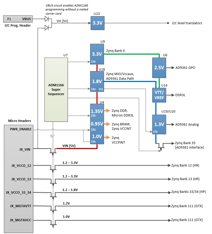
Eight regulators reside on the AD9361-Z7035 SOM that provide a variety of voltage rails required for the Zynq SoC, the AD9361, and their supporting circuitry. These regulators are powered from the end user carrier card through the VIN pins on the SOM Micro Headers - either by direct connection to VIN or derived by cascaded regulators on the SOM. The image below shows a simplified view of the overall power scheme.
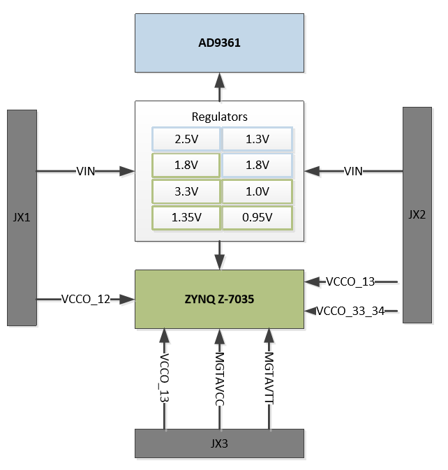
This image summarizes the voltage regulation and connections.
Monitor and Sequencing
AD9361-Z7035 2X2 uses the ADM1166 Super Sequencer (U7) to implement a complete supervisory and sequencing system to ensure all power rails are energized in the required order and maintain regulation. If the SOM detects any of its voltage rails are outside of normal regulation, it will disable all regulators to protect the module from damage.
This functionality is also valuable for designers needing built-in self-test (BIST) capabilities for the SOM once deployed in an end product. The system also makes available supply margining capabilities using the Analog Devices ADM1166. Margining can be useful for testing system regulation and for reducing voltage to certain components during low activity to reduce system power.
While the ADM1166 continuously monitors the critical SOM voltage rails, those not monitored directly by the ADM1166 are measured by an AD7291 ADC (U24). Both devices are connected via I2C to Zynq PL Bank 13 for monitor of all voltage rails with an embedded application. The I2C signals are also brought to the SOM JX micro headers for connection to a carrier card. The ADM1166 non-volatile memory can be re-programmed. The image below provides a detailed timing diagram of the system voltage sequencing, but rest assured that the carrier may supply voltages to the SOM in any order.
Zynq Power Supply Sensors: The Zynq SoC on-chip XADC includes a temperature sensor and power supply sensors that capture the voltage level of VCCINT, VCCAUX, VCCBRAM, VCCPINT, VCCPAUX, and VCCO_DDR. These values are captured in registers that may be read by the Zynq ARM processors. Please see Xilinx UG480 for details.
Power Good Signal: The SOM provides a PG_MODULE signal to the JX micro headers for use on the carrier card to indicate when all of the SOM power supplies are on line. For example, this may be used to enable other power supply circuits on the carrier. The PG_MODULE signal has a 10kΩ pull-up to VIN on the SOM. When PG_MODULE is released by the ADM1166 (U7), a power good LED (D3) will illuminate on the SOM. .
Power Good LED: The SOM uses the PG_MODULE signal to illuminate a green LED (D3) to provide visual status information about the ADM1166 sequencer state machine.
Table 23 - Power Good LED Status
Power cycle the board to reset the ADM1166 state machine
(1) Feature included on Rev D and later
Note: The toggling feature for PG_MODULE was introduced with REV D modules. If the toggling behavior of PG_MODULE is undesirable in your system, the ADM1166 firmware may be modified to remove it.
Power Enable Signal: The carrier card can provide a PWR_ENABLE signal to the module (a so-called “C2M” signal). When the SOM observes that this signal is pulled low, the ADM1166 state machine will not enable any power supplies. Only VIN will be energized on the module, but no downstream regulators will be enabled until PWR_ENABLE is released. This signal has a 10kΩ pull-up to VIN on the SOM.
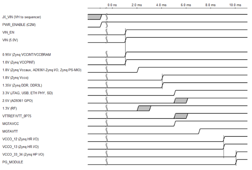
Power Sequencing (Rev D firmware)
Power Estimation
The total power consumption of the AD9361-Z7035 2X2 SOM depends on many factors, but not surprisingly the dependencies are mostly related to the way the Zynq SoC and AD9361 are programmed. The most difficult to predict is the Zynq SoC power consumption, which can vary widely depending upon the configuration of the Zynq PS and its peripherals, and the Zynq PL logic utilization and frequency of operation. Xilinx provides a suite of software tools and documentation to help you evaluate the thermal and power supply requirements of the entire Zynq SoC.
The Xilinx Power Estimator (XPE) is a spreadsheet-based tool that estimates the power consumption of your design. It accepts design information through simple design wizards, analyzes them, and provides a detailed power and thermal information. See Xilinx UG440 for details and download the XPE Tool here.
The Xilinx Vivado Design Suite power analysis feature performs power estimation automatically based on your implemented design. In addition, it can use simulation results to more accurately estimate power based on your expected toggle rates. See Xilinx UG907 and Xilinx UG997.
The SOM power system was designed to supply sufficient power to the Zynq Z-7035 SoC, the AD9361, and all on-board peripherals using demanding radio use case scenarios, including implementation of a full LTE Media Access Controller (MAC) in the Zynq PL. Of course, the carrier must supply VIN (5.0V) to power the SOM regulators, and therefore must be sized according to the demand of your design. The Zynq user bank I/O voltages are powered from the carrier, but only as needed by your design.
Battery Backup for Device Secure Boot Encryption Key
Zynq power rail VCCBATT is a 1.0V to 1.89V voltage, typically supplied by a battery. This supply is used to maintain an encryption key in battery-backed RAM for device secure boot. The encryption key can alternatively be stored in eFuse which does not require a battery.
As specified in the Zynq TRM, if the battery is not used, connect VCCBATT to either ground or VCCAUX. On the AD9361-Z7035, VCCBATT is connected through a 0 Ω resistor (R9) to the AD9361-Z7035 VCCAUX supply (VCCPCOM-1P8V), which is 1.8V. In parallel, the net FPGA_VBATT connects to the VCCBATT pin and is extended to the JX1 micro header for connection on a carrier card.
Important
To apply an external VCCBATT battery to Zynq from the end user carrier card, remove R9 from the AD9361-Z7035 System-On-Module.