AD-FMCOMMS11-EBZ Characteristics & Performance
Both Transmitter and Receiver were characterized independently. A comprehensive characterization suit of tests are reported upon herein. Characterization consists of SFDR, band flatness, IMD/ACLR and NSD measurements for each of the bands under consideration. These bands are 8 (925-960 MHz), 3 (1805 – 1880 MHz), 10 (2110 – 2170 MHz), 7 (2620 – 2690 MHz) and 22 (3510 - 3590 MHz).
Band |
TX Band (MHz) |
Expanded TX Band (MHz) |
|---|---|---|
8 (GSM) |
925-960 |
855-1030 |
3 (GSM) |
1805-1880 |
1655-2030 |
10 (LTE) |
2110-2170 |
1990-2290 |
7 (LTE) |
2620-2690 |
2480-2830 |
22 (LTE) |
3510-3590 |
3350-3750 |
The following equipment were used:
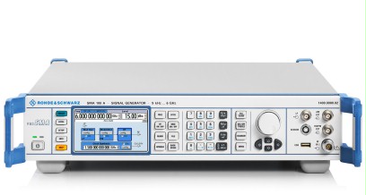
R&S SMA 100A signal gen (range:9kHz – 6GHz)
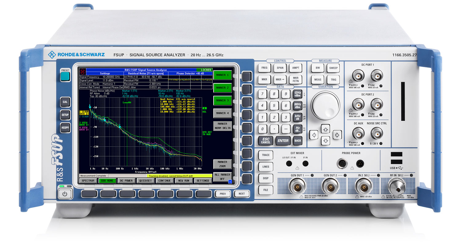
R&S®FSUP Signal Source Analyzer (upto 26.5GHz)
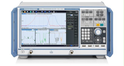
R&S ZND Vector Network Analyzer
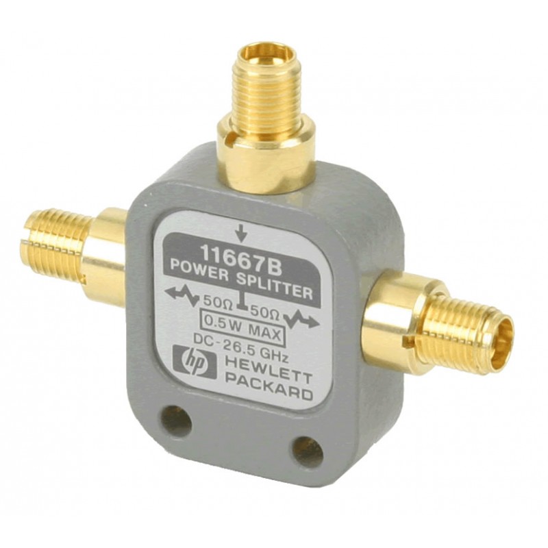
11667B Power Splitter, DC to 26.5 GHz
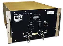
K&L SPCL-00310 Microwave Tunable Filter (15 MHz to 4 GHz)
Receive Channel
Digital Step Attenuator (DSA) Frequency Response Test
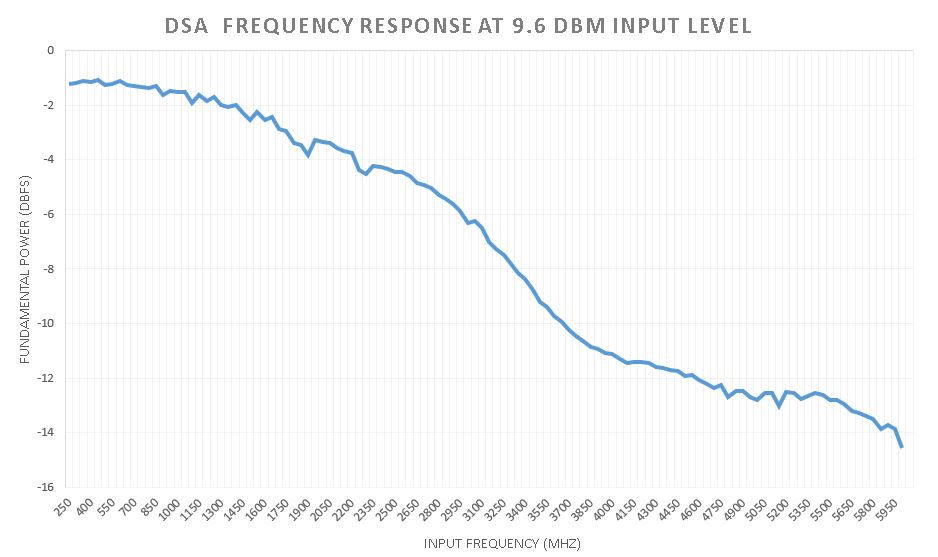
The following images show the DSA (HMC1119) response with respect to the frequency with fix input power 9dBm and varying input frequency range (200MHz-6000MHz) of the receive channel. The table and image shows the following results:
Case |
Response |
|---|---|
At -3dBFS Point |
2150MHz |
At 250MHz |
-1dBFs |
At 4GHz |
-11.4dBFs |
At 6GHz |
-14.5dBFs |
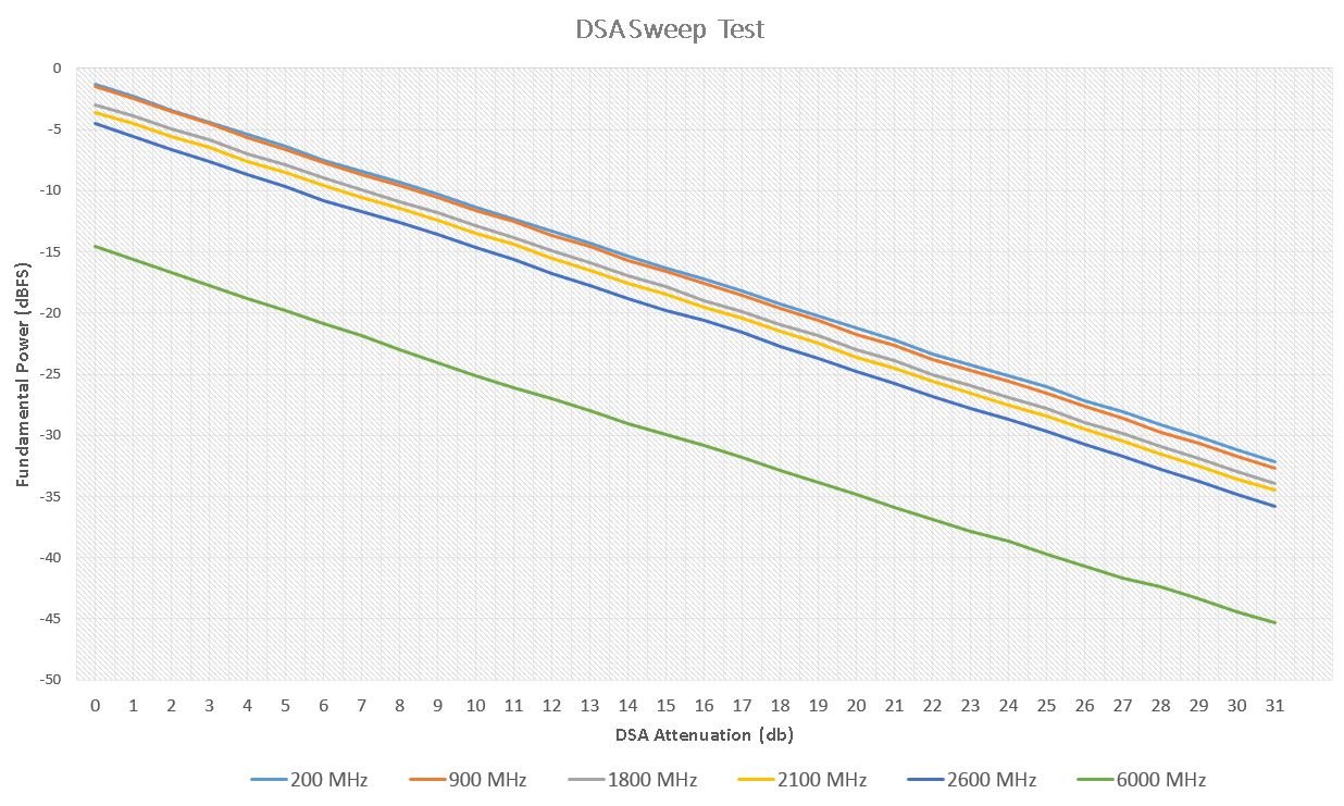
Another test was conducted by varying the attenuation level linearly with respect to a chosen input frequency from a signal generator. The table and image shows the following results:
DSA Sweep Frequency (MHz) |
(dBFS) |
|---|---|
200 |
0.256 |
900 |
0.337 |
1800 |
0.29 |
2100 |
0.384 |
2600 |
0.55 |
6000 |
1.505 |
Single Tone Test
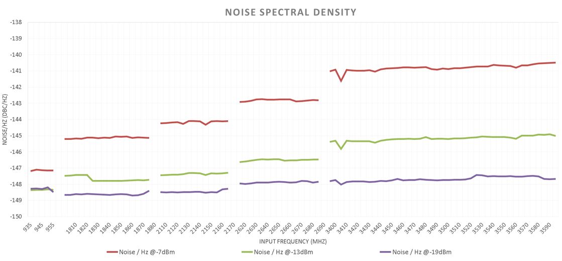
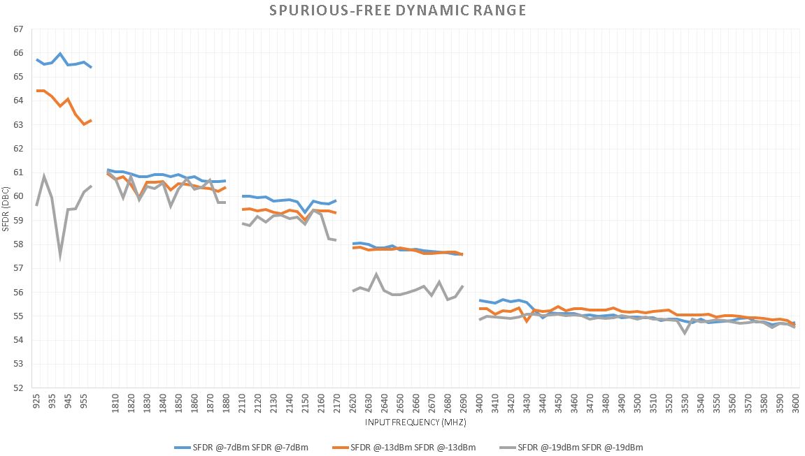
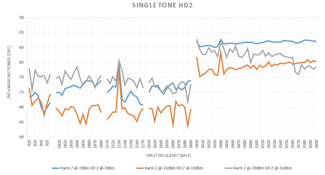
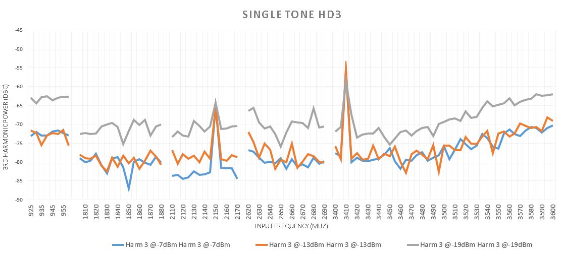
A single tone at three different power levels, -7, -13 and -19 dBm, is injected into a configurable band pass filter before going to the receiver input of the board to measure the NSD, SFDR, HD2 and HD3.

Noise Spectral Density (NSD) Test
The following figure shows the noise spectral density with varying input power in dBFs.
Spurious-Free Dynamic Range (SFDR) Test
The following figure shows the spurious-free dynamic range with varying input power in dBFs.
Single Tone 2nd Harmonic Distortion (HD2) Test
The following figure shows the 2nd harmonic distoriton with varying input power in dBFs.
Single Tone 3rd Harmonic Distortion (HD3) Test
The following figure shows the 3rd harmonic distoriton with varying input power in dBFs.
Two Tone Test
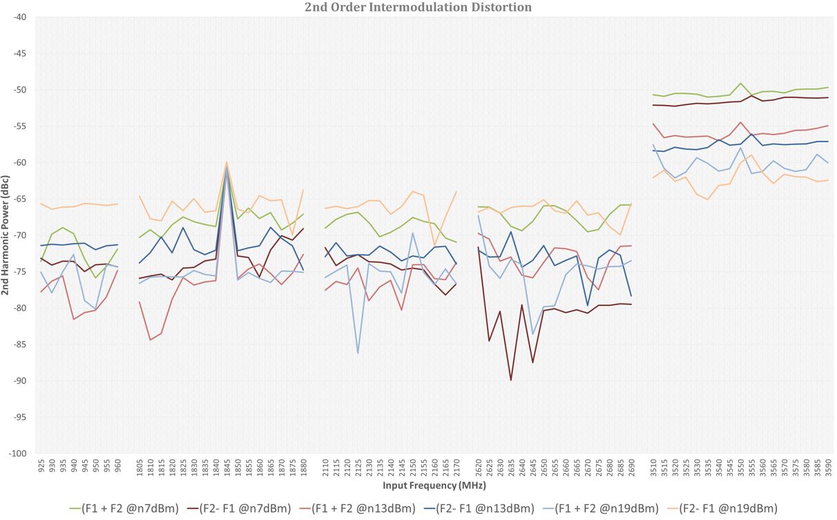
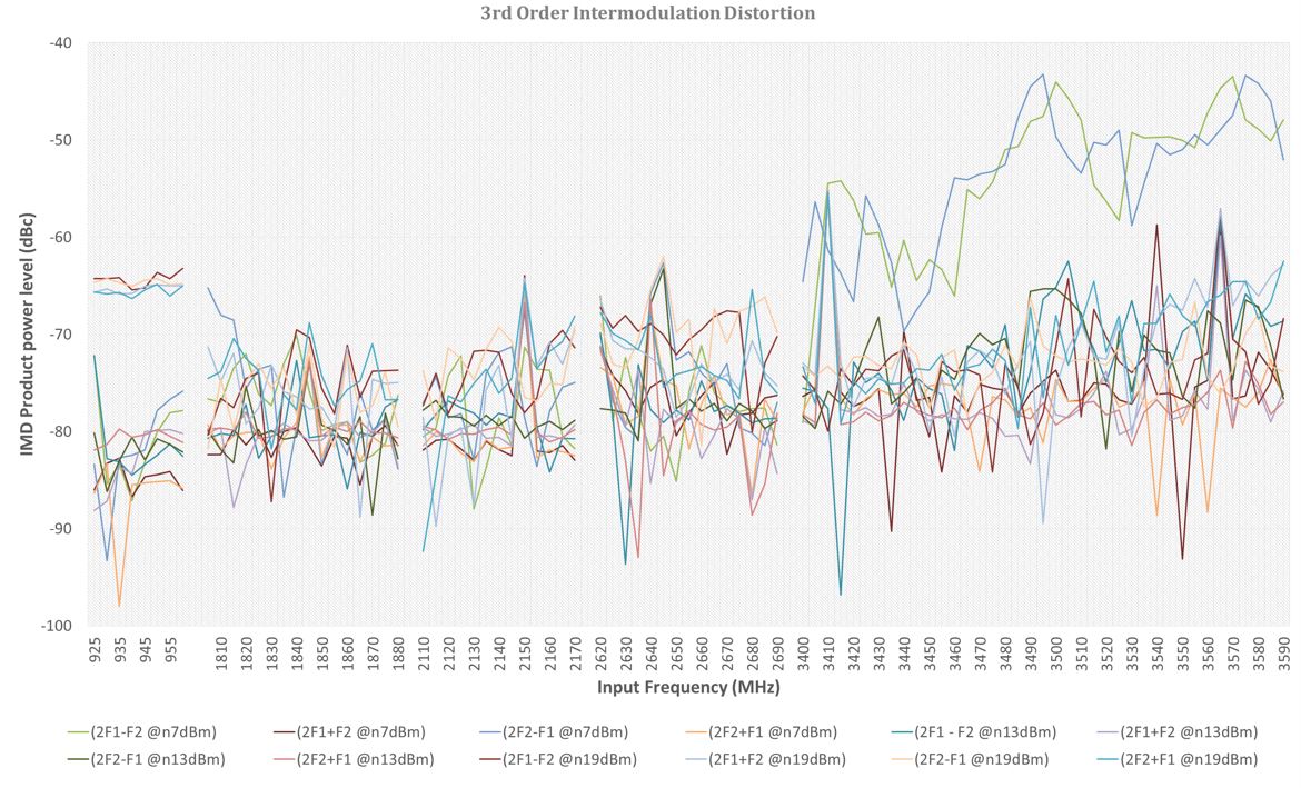
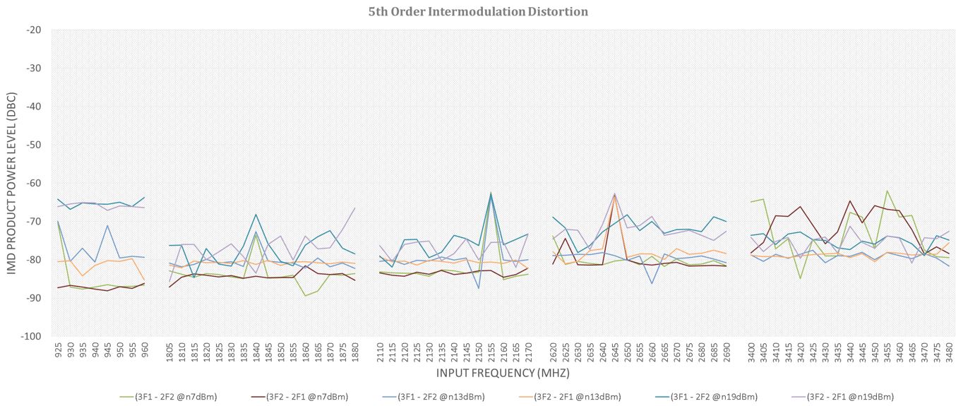
Two tones with 3 MHz in between spacing is swept across all bands at 5 MHz intervals at three different power levels -7, -13 and -19 dBm. The combined signal is the input to the K&L filter and the output of this filter will be the input to the ADC. IMD2, IMD3 and IMD5 performance is measured
Two SMA100A was used to produce the tones with 3 MHz spacing. These two tones are the inputs to the combiner which outputs the two tone signal combination. This two tone goes through the K&L filter to clean out any unnecessary noise before the ADC input.

Two Tone 2nd Order Intermodulation Distortion(IMD2) Test
The following figure shows the 2nd harmonic distoriton with varying input power in dBFs.
Two Tone 3rd Order Intermodulation Distortion(IMD3) Test
The following figure shows the 3rd harmonic distoriton with varying input power in dBFs.
Two Tone 5th Order Intermodulation Distortion(IMD5) Test
The following figure shows the 5th harmonic distoriton with varying input power in dBFs.
Return Loss (S11) Test
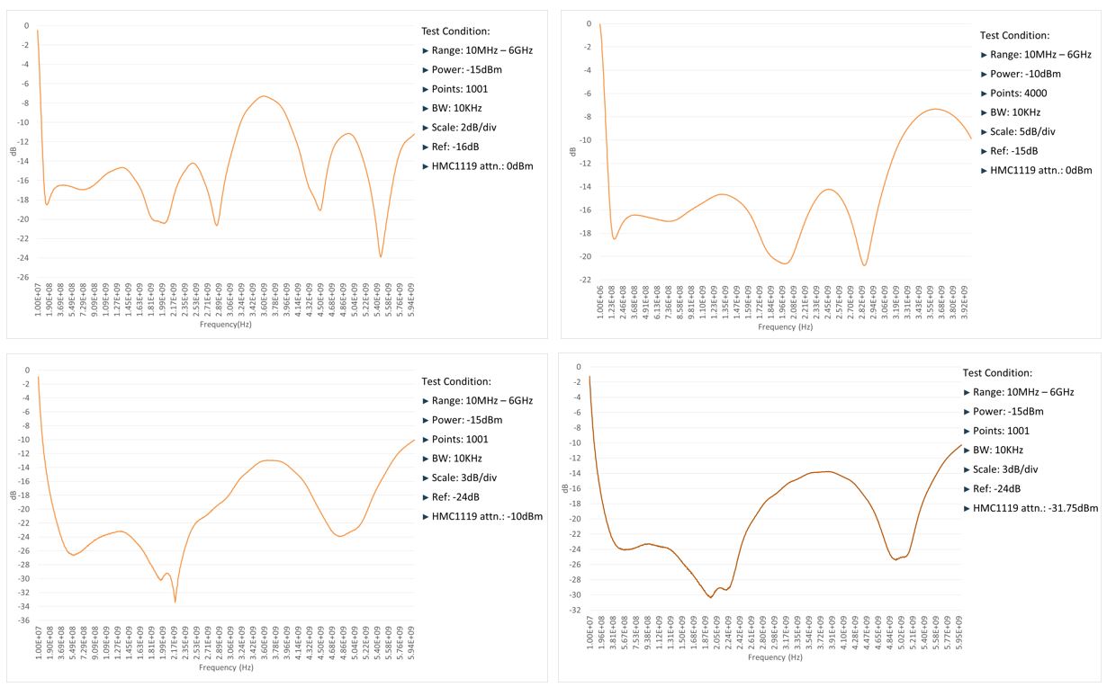
There are 4 test settings to be done and the VNA needs to be calibrated every time there is change in test settings. The settings for each test is shown in Table 1. These settings are for the VNA and DSA.
Test Parameters |
Test 1 |
Test 2 |
Test 3 |
Test 4 |
|---|---|---|---|---|
Range |
10 MHz – 6 GHz |
1 MHz – 4 GHz |
10 MHz – 6 GHz |
10 MHz – 6 GHz |
Power |
-15 dBm |
-10 dBm |
-15 dBm |
-15 dBm |
Points |
1001 |
4000 |
1001 |
1001 |
Bandwidth |
10 kHz |
10 kHz |
10 kHz |
10 kHz |
Scale |
2 dB/div |
5 dB/div |
3 dB/div |
3 dB/div |
Reference level |
-16 dB |
-15 dB |
-24 dB |
-24 dB |
DSA attenuation |
0 dBm |
0 dBm |
-10 dBm |
-31.75 dBm |
The following figure shows the return loss obtained using R&S ZND Vector Network Analyzer(VNA).
Transmit Channel
Dual band tests were conducted as well as this architecture is thought to be conducive to multiband transmission. A set of band pairs where investigated through band flatness, SFDR and IMD/ACLR.
The following table shows the DAC settings used during the test.
DAC Parameters |
DAC Settings |
|---|---|
F_dac_clock (MHz) |
4915.2 |
Mode |
DDR On, Mix off |
Interpolation |
4x, complex |
Bit rate per lane (Gbps) |
6.144 |
Lanes |
8 |
F_data(MSps) |
1228.8 |
NCO |
Tes/band dependent |
Output Frequency Band Flatness Test
The frequency response was analyzed. A single tone at -12 dBFS is swept from 20 MHz to 4.8 GHz in 2 MHz steps. For simplicity sake, the DAC was placed in NCO mode for this test.
Case |
Response |
|---|---|
At 3dB Point |
1.5GHz |
At 6dB Point |
4GHz |
Flatness Range |
1.5GHz - 3GHz |
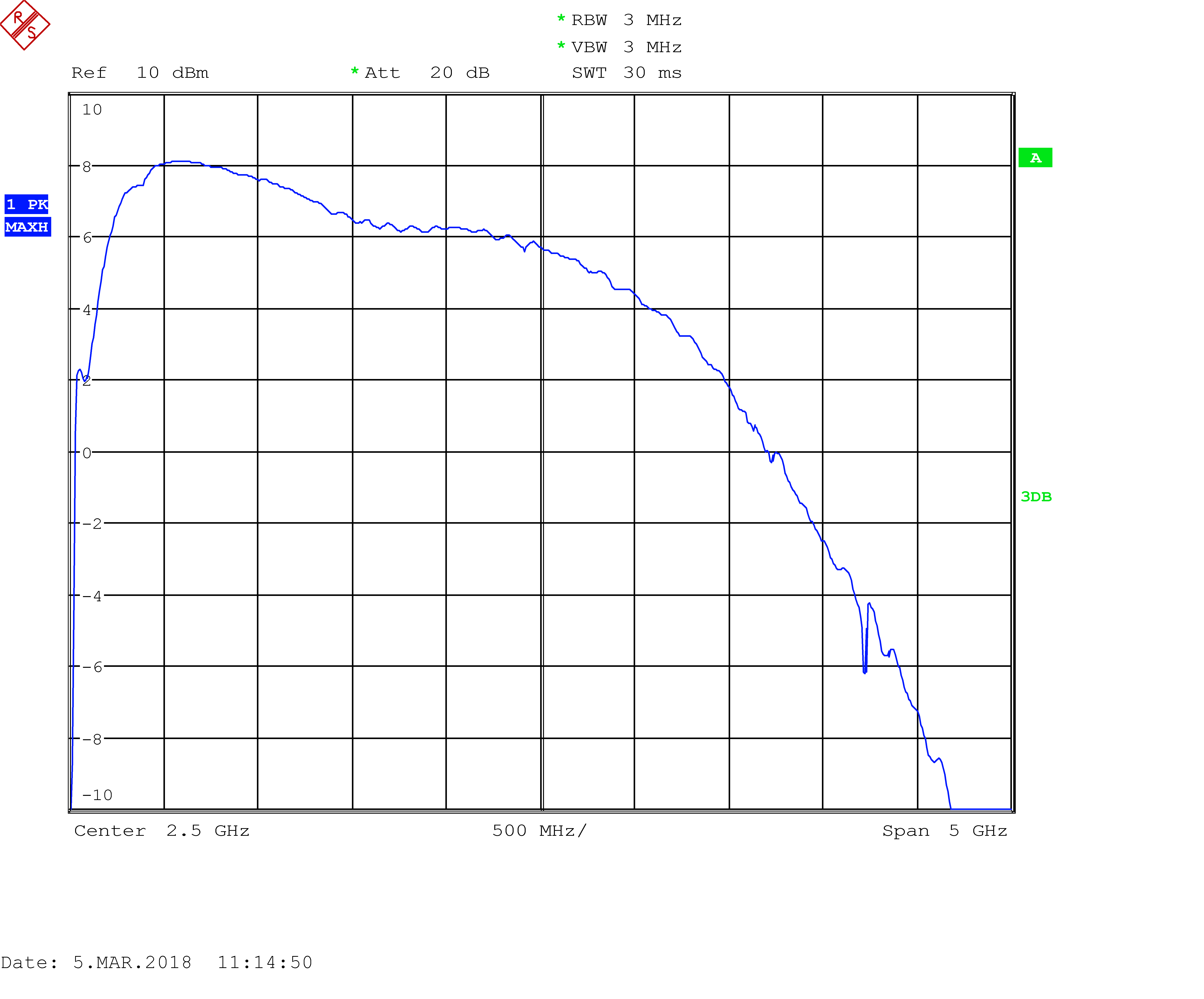
The following results show the flatness response of the DAC at different bands:
Band |
TX In-Band (dB) |
Expanded TX Band (MHz) |
|---|---|---|
8 |
0.1 |
0.3 |
3 |
0.1 |
0.3 |
10 |
0.1 |
0.5 |
7 |
0.2 |
1.0 |
22 |
0.7 |
4.0 |
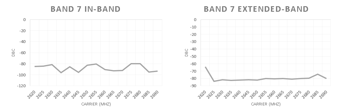
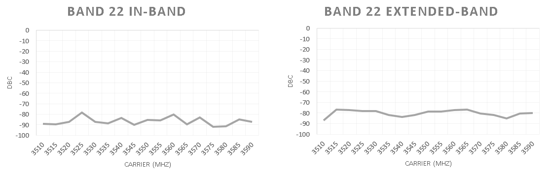
Spurious-Free Dynamic Range (SFDR) Test
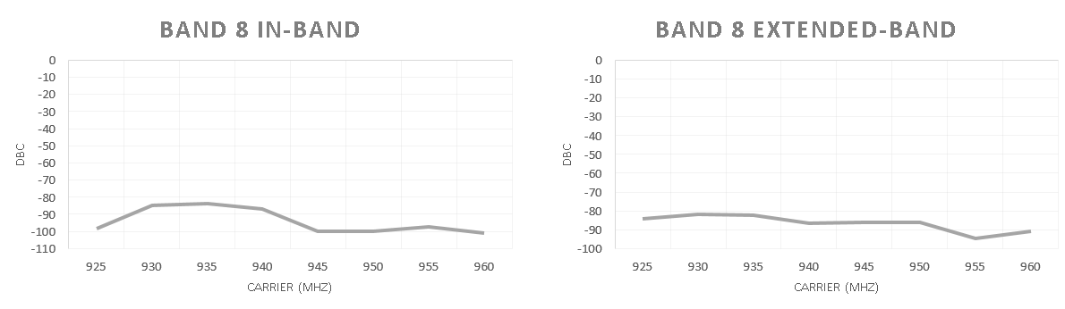
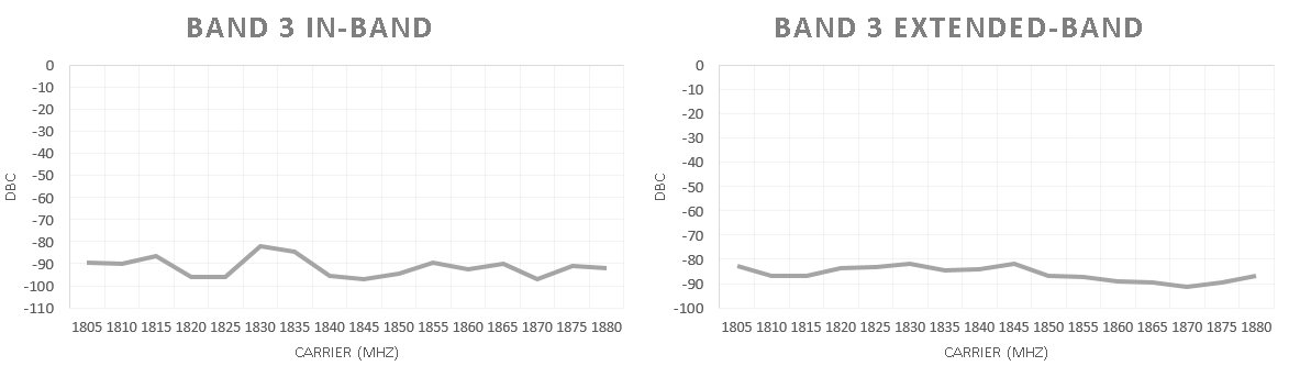
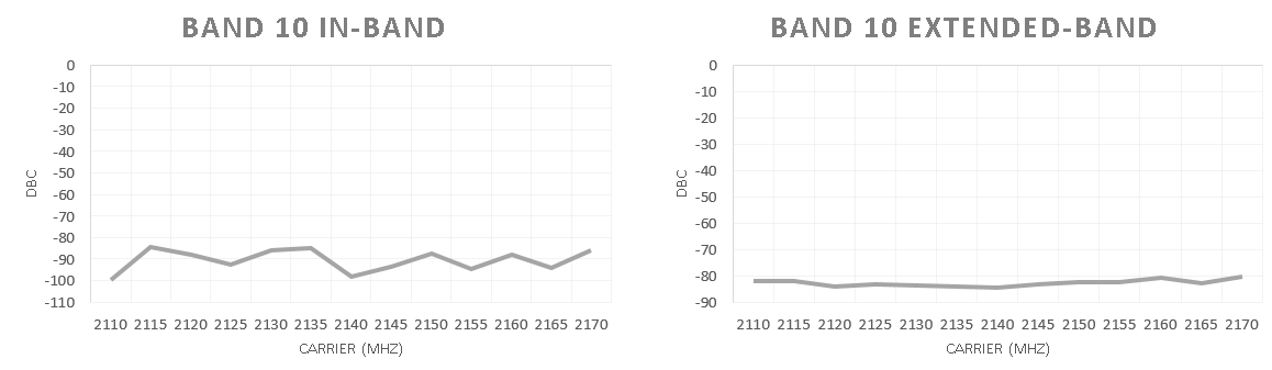
SFDR was measured by stepping an integration interval over the expanded band of interest in Table 7. The integration bandwidth is 100 kHz or 5 MHz for GSM and LTE, respectively. For each sweep, the fundamental is stepped in 5 MHz increments by changing the NCO.
EDGE GSM vector properties |
LTE vector properties |
|---|---|
Single carrier |
Single 5 MHz carrier |
Centered on 0 Hz |
Centered on 0 Hz |
PAR of 6.82 dB |
PAR of 10.52 dB |
Plus digital back-off of 5.14 dB for -12 dBFS |
Plus digital back-off of 1.6 dB for -12 dBFS |
Noise Spectral Density(NSD) Test
Block Diagram of the Test Setup

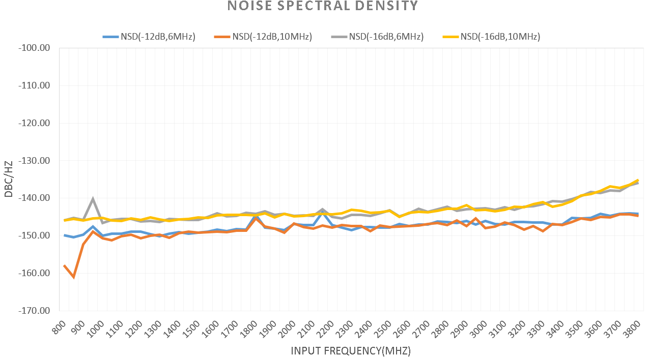
Noise spectral density was measured at an offset from a single tone, generated in NCO mode, at each band center. Measurement is done over an integration bandwidth of 500 kHz with a stock PXA without any special phase noise measurement module. Attenuation is set to 2-4 dB.
Inter-Modulation Distortion(IMD) Test
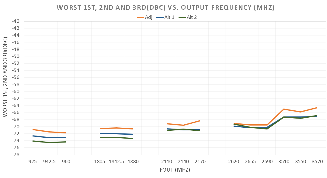
For IMD measurements, ACLR is used. The signals used are outlined in table below; they are the worst case IMD of each respective band. Only the band edges and the mid-band cases were measured. Graphs are shown below. Both the GSM and LTE vectors have a PAR of around 11 dB and are given one more dB of digital back-off to reach -12 dBFS. The NCO is used to place the signal to its final location.
Carrier Settings
Band |
# of TX Channel |
# of Adj channel |
Integration Bandwidth |
Carrier Separation |
|---|---|---|---|---|
GSM |
6 |
3 |
30KHz |
600KHz |
LTE |
2 |
3 |
18MHz |
40MHz |
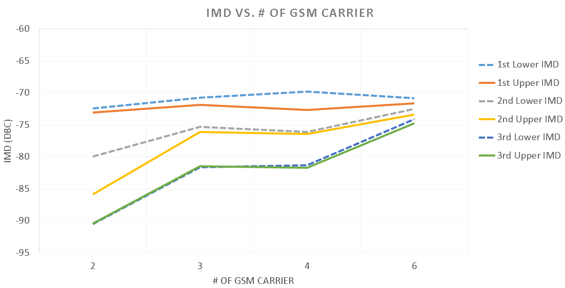
Shown below is the IMD performance with varying number of carrier for GSM band. This sweep was done at the center of band 8.