ADAQ23876/ADAQ23878 User Guide
Evaluating Using ZedBoard
Features
Evaluation Requirements
Hardware
EVAL-ADAQ23876FMCZ or EVAL-ADAQ23878FMCZ evaluation board
12V power supply
Host PC running Windows 10 or higher
SD Card (16GB or larger)
LAN Cable
SMA Cable
XLR to SMA adapter cable
Audio Analyzer (Audio Precision APX525) or other input source
Software
General Description
The EVAL-ADAQ23876FMCZ and EVAL-ADAQ23878FMCZ evaluation boards enable performance assessment of the ADAQ23876 and ADAQ23878 15 MSPS, 16-/18-bit, High Speed, Precision µModule Data Acquisition Solutions. These devices incorporate a low noise, fully differential ADC driver, a stable high resolution reference buffer, 16-/18-bit 15 MSPS SAR ADCs, and critical passive components for optimum performance.
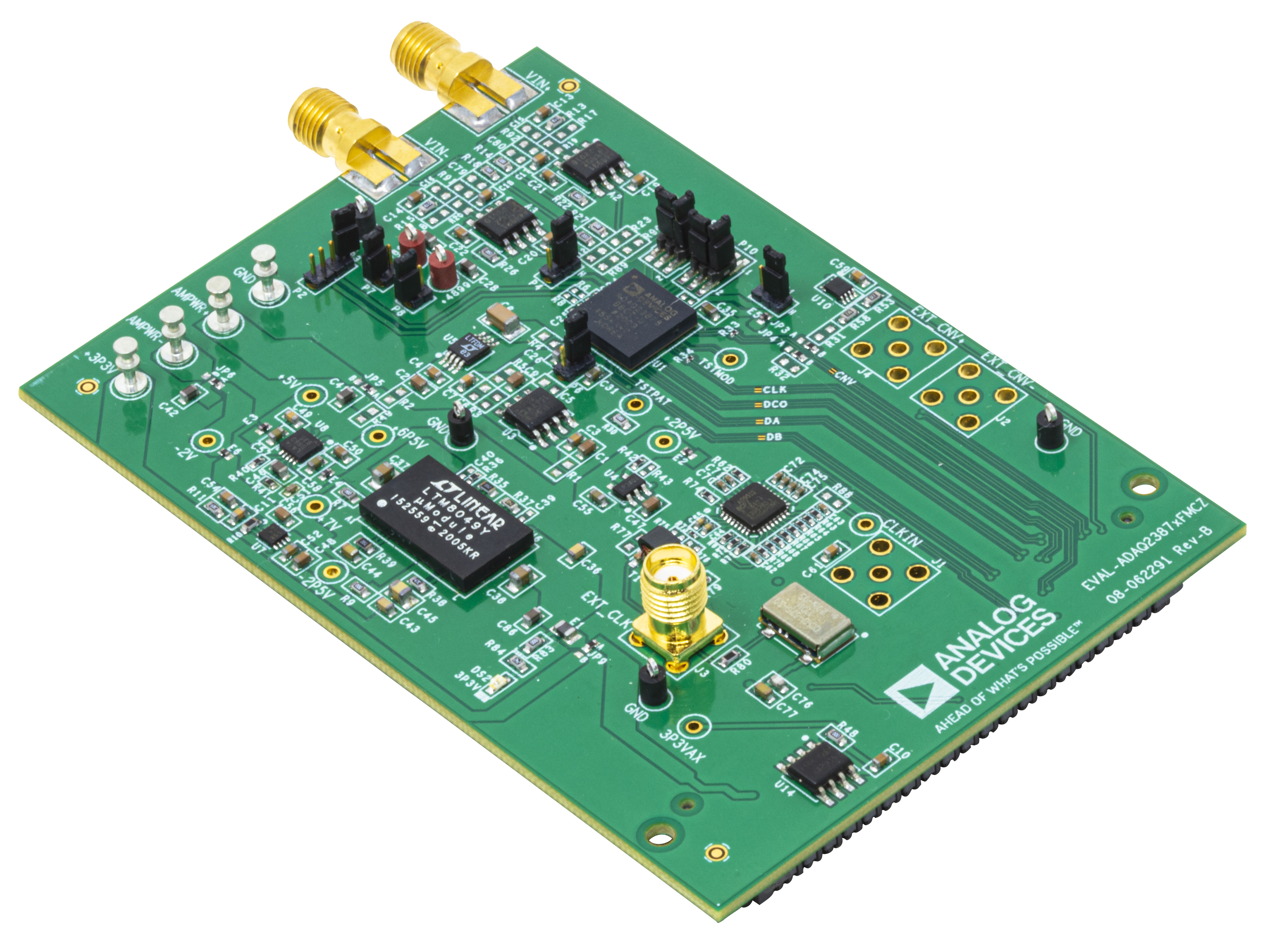
Figure 1 EVAL-ADAQ23876FMCZ / EVAL-ADAQ23878FMCZ Evaluation Board
Getting Started
Setting Up the Evaluation Board
The evaluation board consists of:
Power Supplies
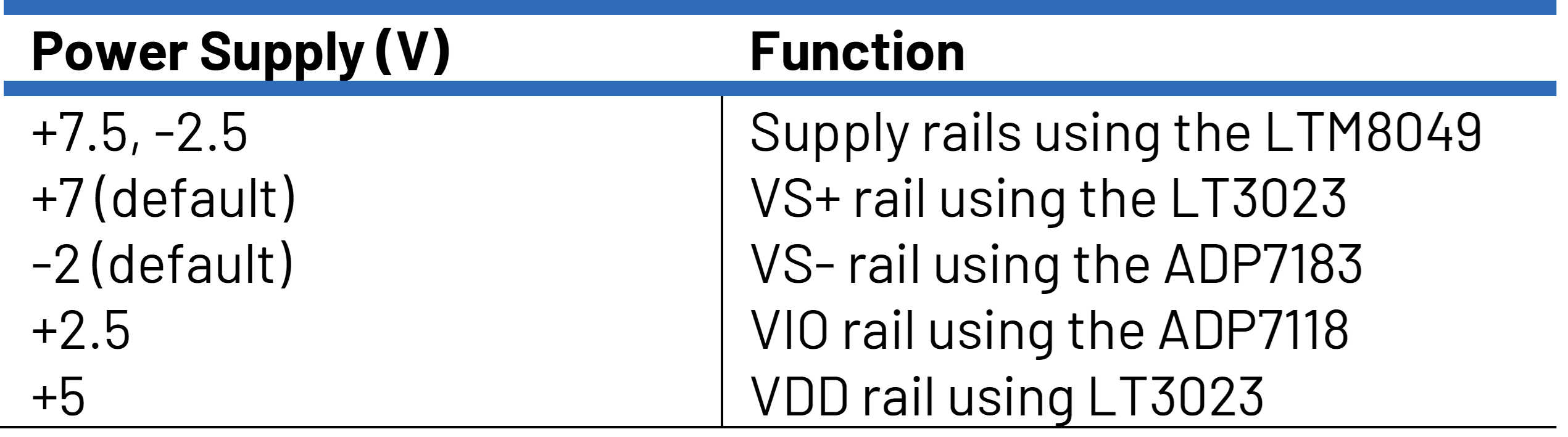
The positive supply rails generated are:
7V (+VS)
5V (VDD)
2.5V (VIO)
The negative supply rail generated is:
−2.0V (−VS)
Components used: LTM8049 (U6), ADP7118 (U4), LT3023 (U8), ADP7183 (U7).
Each supply rail has the necessary decoupling capacitors placed as close as possible to the device. A single ground plane is used to minimize the effect of high-frequency noise interference.
Analog Inputs
Subminiature Version A (SMA) connectors (VIN+ and VIN−) provide analog inputs from a low-noise, audio precision signal source (SYS-2700 or SYS-x555 series).
Two configuration options are available:
Direct signal feed to the ADAQ23876/ADAQ23878, bypassing A2 and A3.
Through the optional ADA4899-1 amplifiers (A2, A3) in unity-gain configuration, driving the ADAQ23876/ADAQ23878.
The default board configuration provides 4.096V on the REFBUF pin and a buffered 2.048V (midscale) at the VCMO (FDA) pin.
Note
For input frequencies below 100 kHz, use a low-noise audio precision signal source (SYS-2700 series) with outputs set to balanced floating.
Link Options

Figure 3 Link Options for the EVAL-ADAQ23876FMCZ and EVAL-ADAQ23878FMCZ
Multiple link options must be set correctly before applying power and signal.
Evaluation Board Connector Configuration
Figure |
Gain Setting |
|---|---|
Figure 2 |
Gain = 0.37 |
Figure 3 |
Gain = 0.73 |
Figure 4 |
Gain = 0.87 |
Figure 5 |
Gain = 1.38 |
Figure 6 |
Gain = 2.25 |


Note
User-defined signals: the P suffix denotes the positive pin of a differential pair; the N suffix denotes the negative pin. See the VITA 57 specification.
User-defined signals with the CC suffix are preferred for transmitting clock signals from the controller board to the daughter board. These are connected to global clock lines on the FPGA. See the VITA 57 specification.
Loading the Image onto the SD Card
To properly evaluate the EVAL-ADAQ23876FMCZ / EVAL-ADAQ23878FMCZ, the ADI Kuiper Linux must be properly flashed on the SD card. Complete instructions are available at Kuiper Linux.
Follow the directions for preparing the image specifically for the EVAL-ADAQ23876FMCZ / EVAL-ADAQ23878FMCZ.
SD Card Preparation
Download the ADI Kuiper Image
Follow the instructions at Kuiper Linux. The Kuiper Linux image is an open-source embedded Linux operating system based on Raspberry Pi OS, incorporating Linux device drivers for ADI products.
The ZedBoard can be accessed from a remote PC via LAN cable or Wi-Fi.
Format and Flash the SD Card on Windows hosts
Follow the Windows hosts instructions.
Format and Flash the SD Card on Linux hosts
Follow the Linux hosts instructions.
After flashing, ensure the SD card is configured for the correct FPGA project per the Kuiper Linux documentation.
Copy the following key files to the root folder of the SD card:
BOOT.BINdevicetree.dtbuImage(from thezynq-commonfolder)
Hardware Connection
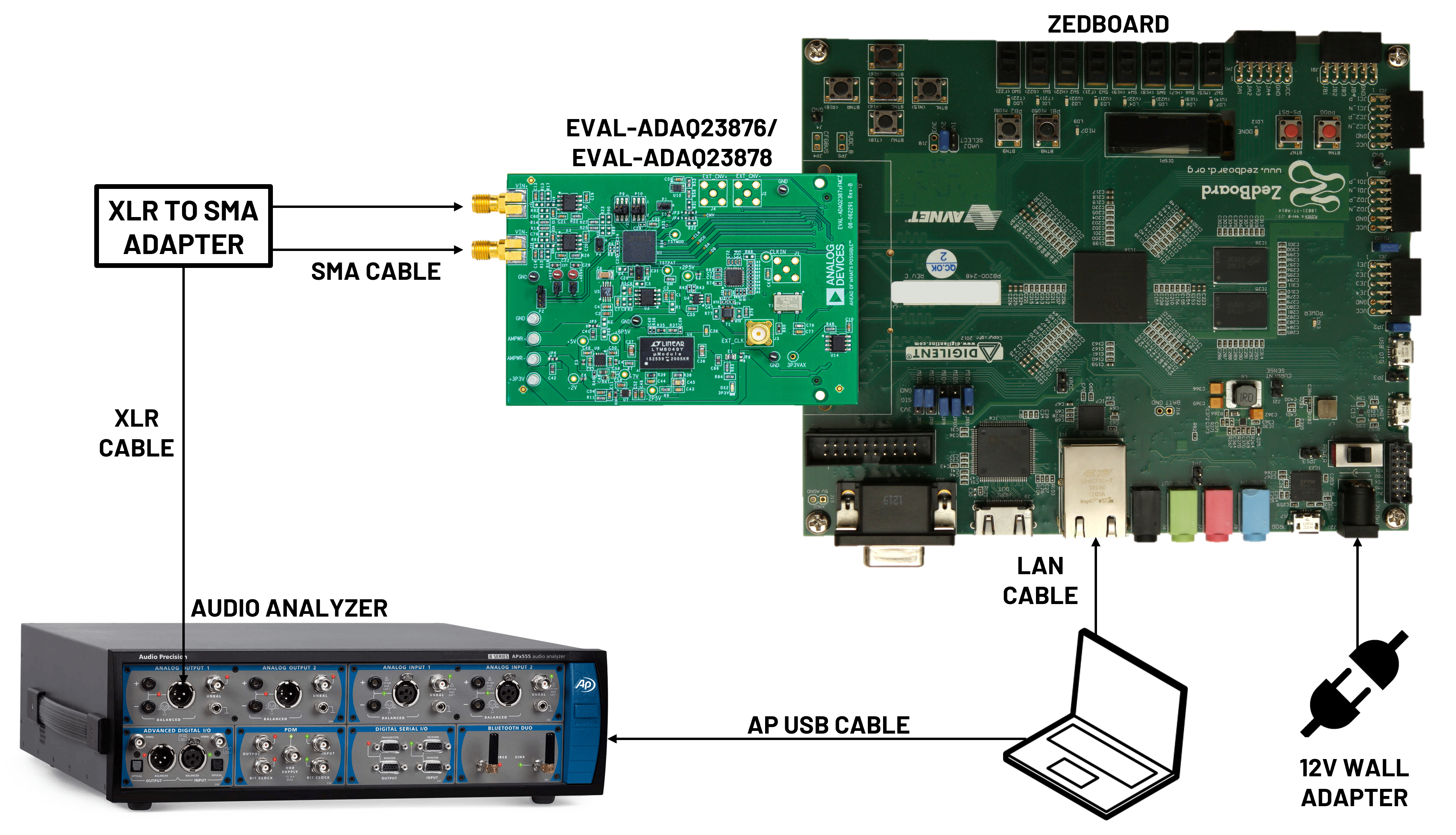
Setup steps (using the Audio Precision Audio Analyzer as input source):
Download and install the IIO Oscilloscope application on the host PC.
Flash the Analog Devices Kuiper Linux image on the SD card.
Properly configure the SD card for the EVAL-ADAQ23876FMCZ / EVAL-ADAQ23878FMCZ.
Insert the SD card into the ZedBoard.
Attach the evaluation board to the ZedBoard through the FMC pin connector.
Power up the ZedBoard using the 12V cable.
Connect the evaluation board to the Audio Precision Audio Analyzer using the XLR to SMA adapter cable.
Connect the Audio Precision Audio Analyzer USB cable to the PC.
Navigating the IIO Oscilloscope
Main Window

The main window displays a configuration panel (plugin) for each device recognized by the system. Additional plugins are loaded for device debugging and monitoring (Debug Tab/Plugin and DMM Tab/Plugin).
Each plugin can be detached by clicking the button on the right side of the plugin name. Close a detached window to re-attach it to the main window.
Debug Tab/Plugin
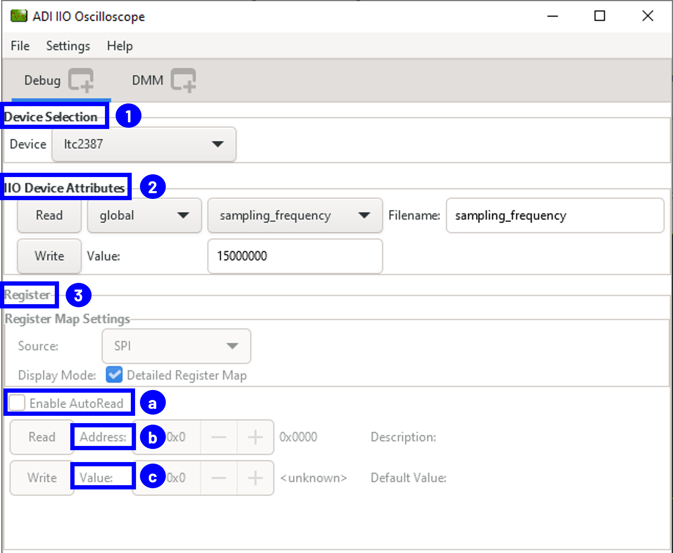
The Debug plugin is a tool for device debugging. Some features may not work unless the oscilloscope application is started as root.
Device Selection: Sets the active device.
IIO Device Attributes: Allows read/write operations for device attributes.
Register: Provides low-level access to device registers.
Enable AutoRead: Allows automatic register reading as the register address changes.
Address: Register address field.
Value: Register value at the given address.
DMM Tab/Plugin
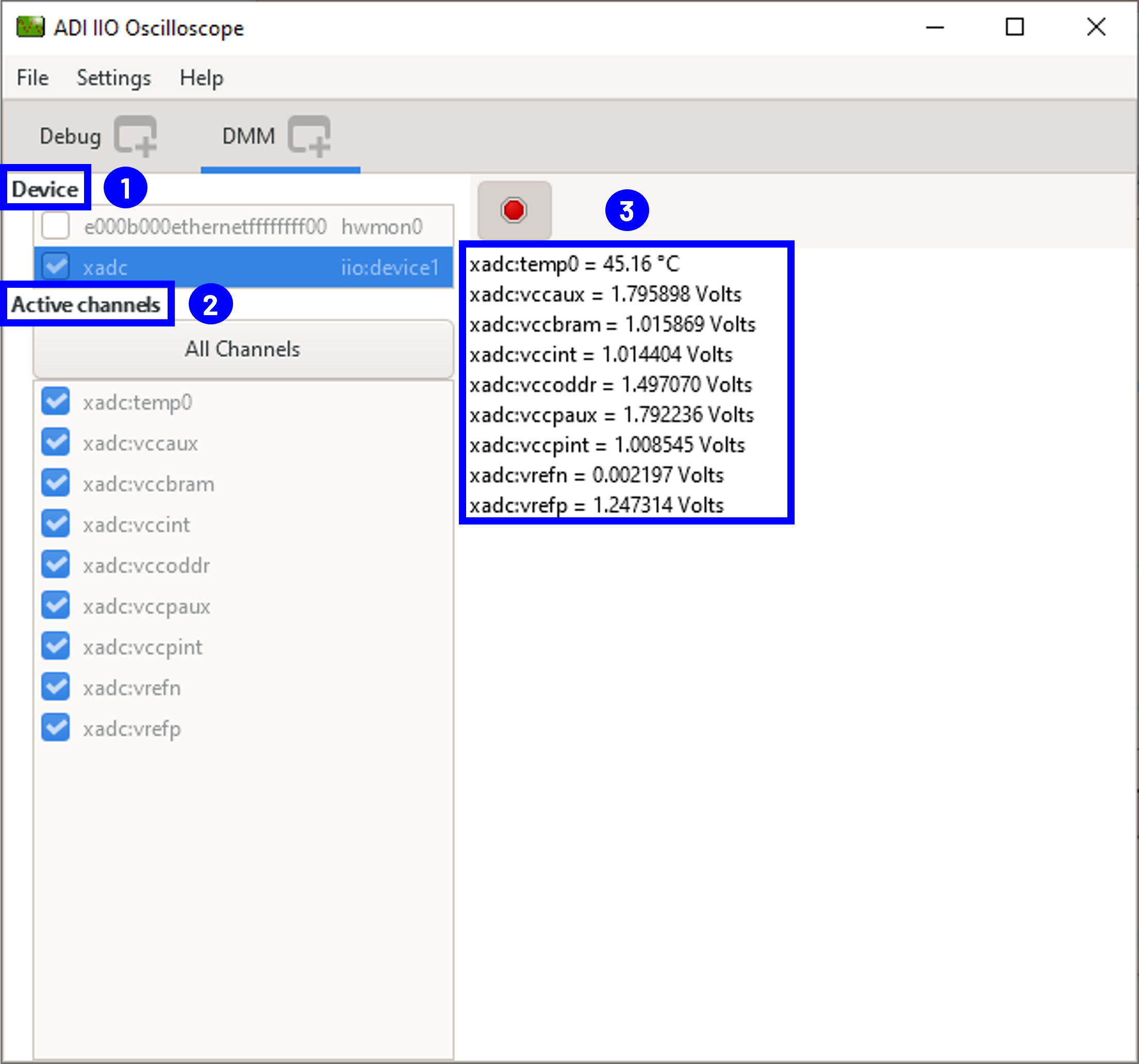
The DMM (Digital Multimeter) plugin displays device-specific data continuously once the start button is activated.
Device tab: Lists all available devices.
Active channels tab: Lists the channels of enabled devices. The “All Channels” button enables all channels simultaneously.
Right side tab: Displays data readings of the enabled channels.
Capture Window
Menu (along top):
File
Save As: Saves data to a file.
Quit: Closes the capture/plot window.
Edit
Plot Title: Changes the window name.
View
Show Settings: Shows/hides the settings panel on the left, allowing the plot to fill the entire window.
Full Screen: Makes the window full screen.
Plot options/icons (along top):
Capture/Stop: Start or stop data capture.
Zoom In: Zoom in on the plot region.
Zoom Out: Zoom out from the plot region.
AutoZoom: Automatic zoom to fit the screen.
Save As: Save data to a file.
FullScreen: Enter/leave fullscreen mode.
Auto scale: Automatically re-scale the visible area to fit the entire plot.
Show grid: Show or hide the grid in the plot window.
Y Max: Adjust the upper limit of the vertical axis (when Auto scale is disabled).
Y Min: Adjust the lower limit of the vertical axis (when Auto scale is disabled).
New Plot: Create a new plot of the same type.
Plot types:
Time Domain
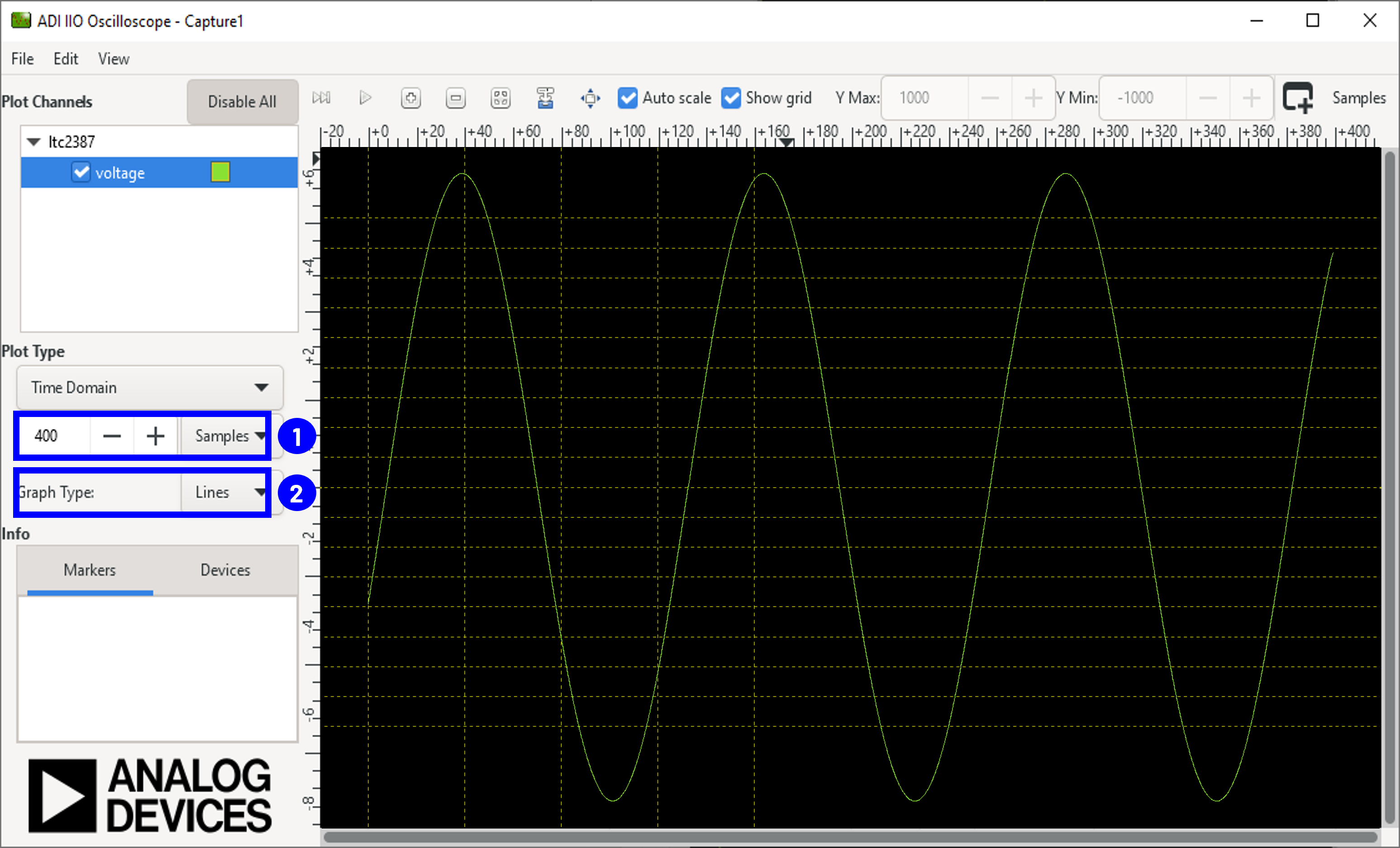
Plots the signal in the time domain. Displays raw samples.
Sample Count: Selects the number of samples for time domain, constellation, and cross-correlation plotting.
Graph Type: Selects the graph type (lines or dots).
Frequency Domain
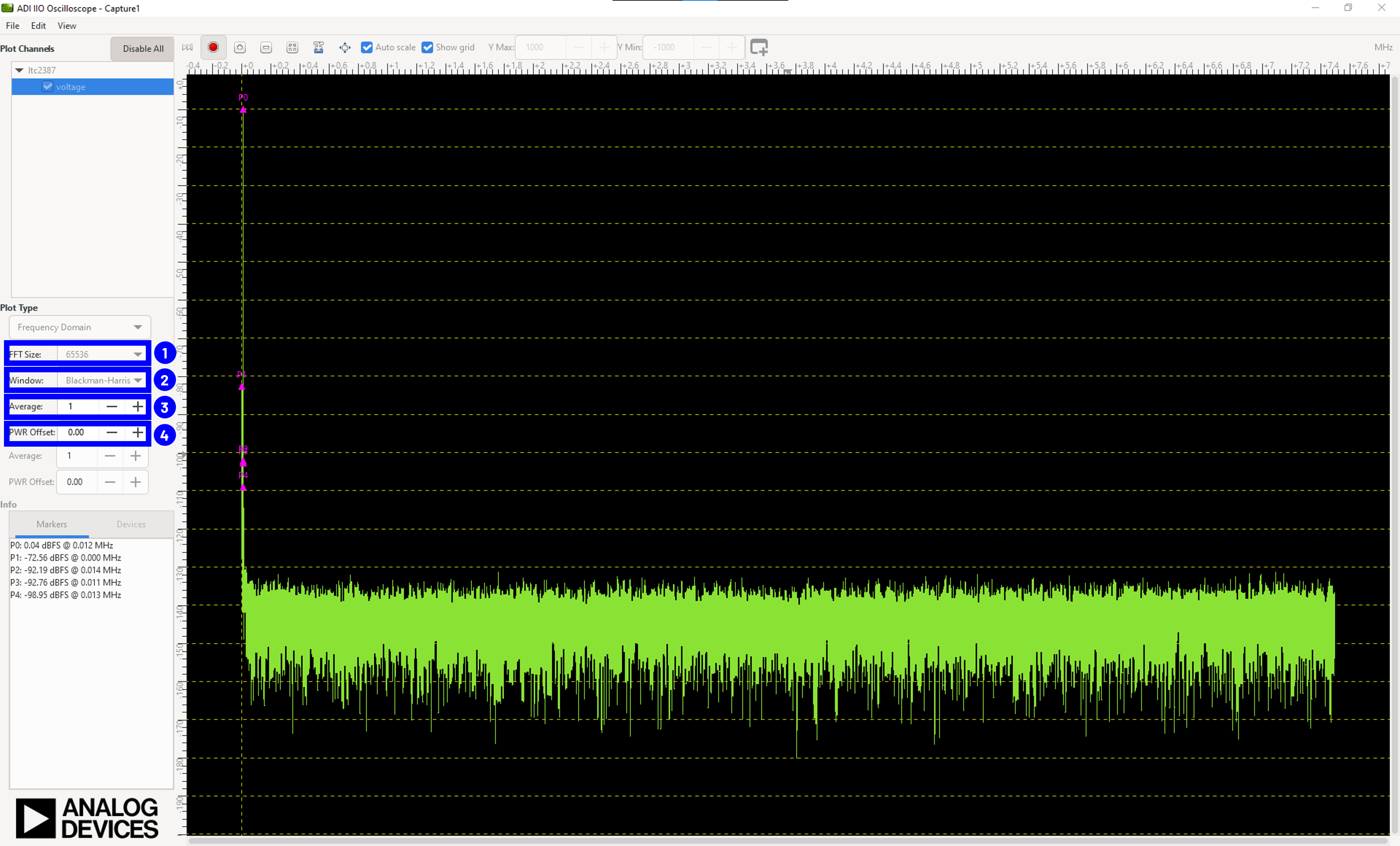
Plots the signal in the frequency domain. Performs an FFT on the signal.
FFT size: Selects the FFT size for frequency domain plotting.
Window: Selects the FFT window function. Each window has its own characteristics and suitability; see the window functions page.
FFT Average: Selects the average weight applied to FFT samples.
PWR Offset: Selects the FFT graph offset.
Constellation Plot
Plots the signal as a constellation plot, with the I-channel on the x-axis and the Q-channel on the y-axis.
Sample Count: Selects the number of samples.
Graph Type: Selects the graph type (lines or dots).
Cross Correlation Plot
Plots the signal as a cross-correlation plot.
Sample Count: Selects the number of samples.
Graph Type: Selects the graph type (lines or dots).
Activating Markers
Markers are used for plot data measurement in the frequency domain or during cross correlation. Right-click on the plot and select a marker type to enable.
Available marker types:
FFT domain (1 channel enabled): Peak, Fixed, Single Tone
FFT domain (2 channels enabled): Peak, Fixed, Single Tone, Image
Constellation: Peak Marker
Add more markers via Add Marker or remove via Remove Marker.
Saving Captured Data
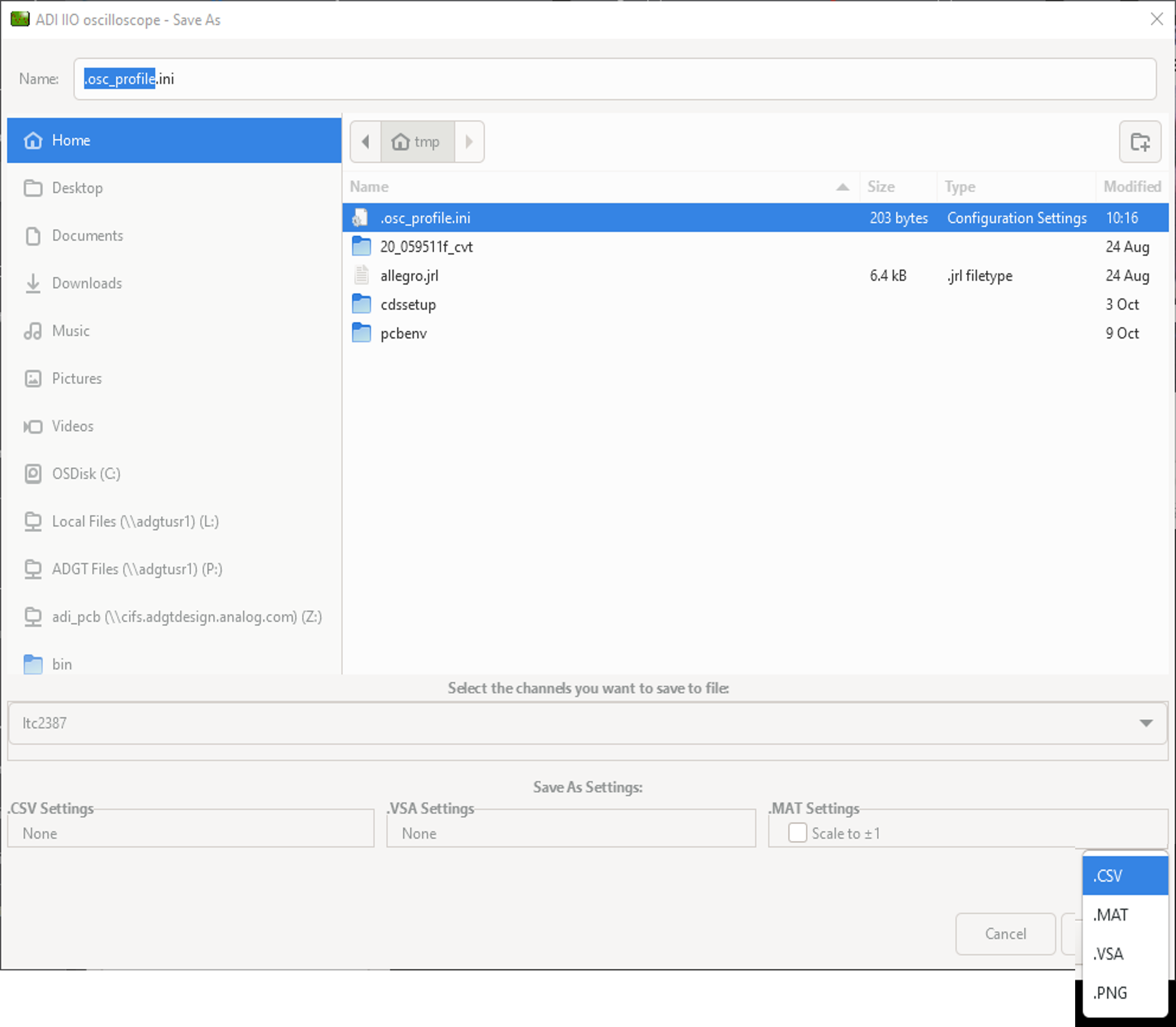
Captured data can be saved in the following formats:
Agilent VSA
CSV (.csv)
MATLAB (.mat)
PNG (.png)
Evaluating the EVAL-ADAQ23876FMCZ / EVAL-ADAQ23878FMCZ Using IIO Oscilloscope
Download the latest release of IIO Oscilloscope.
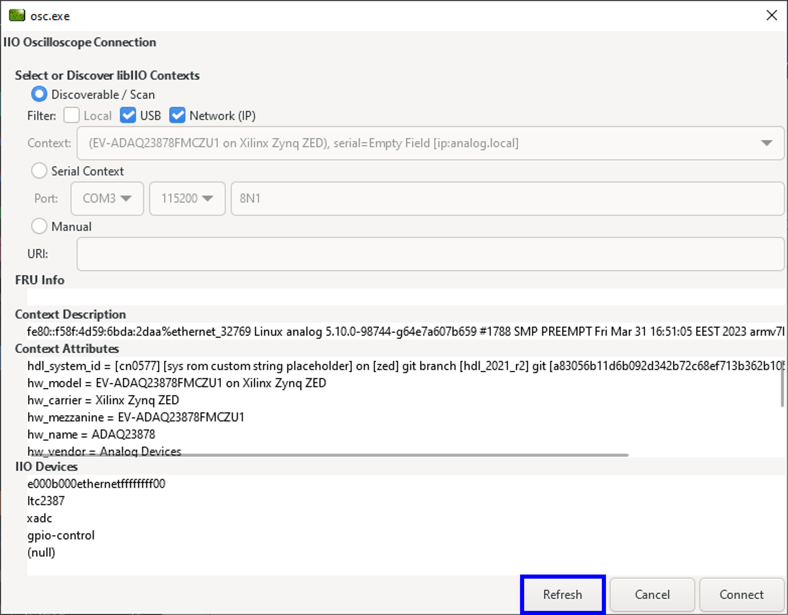
Select the Refresh button to display available IIO devices.
Once
ltc2387appears in the device list, select Connect.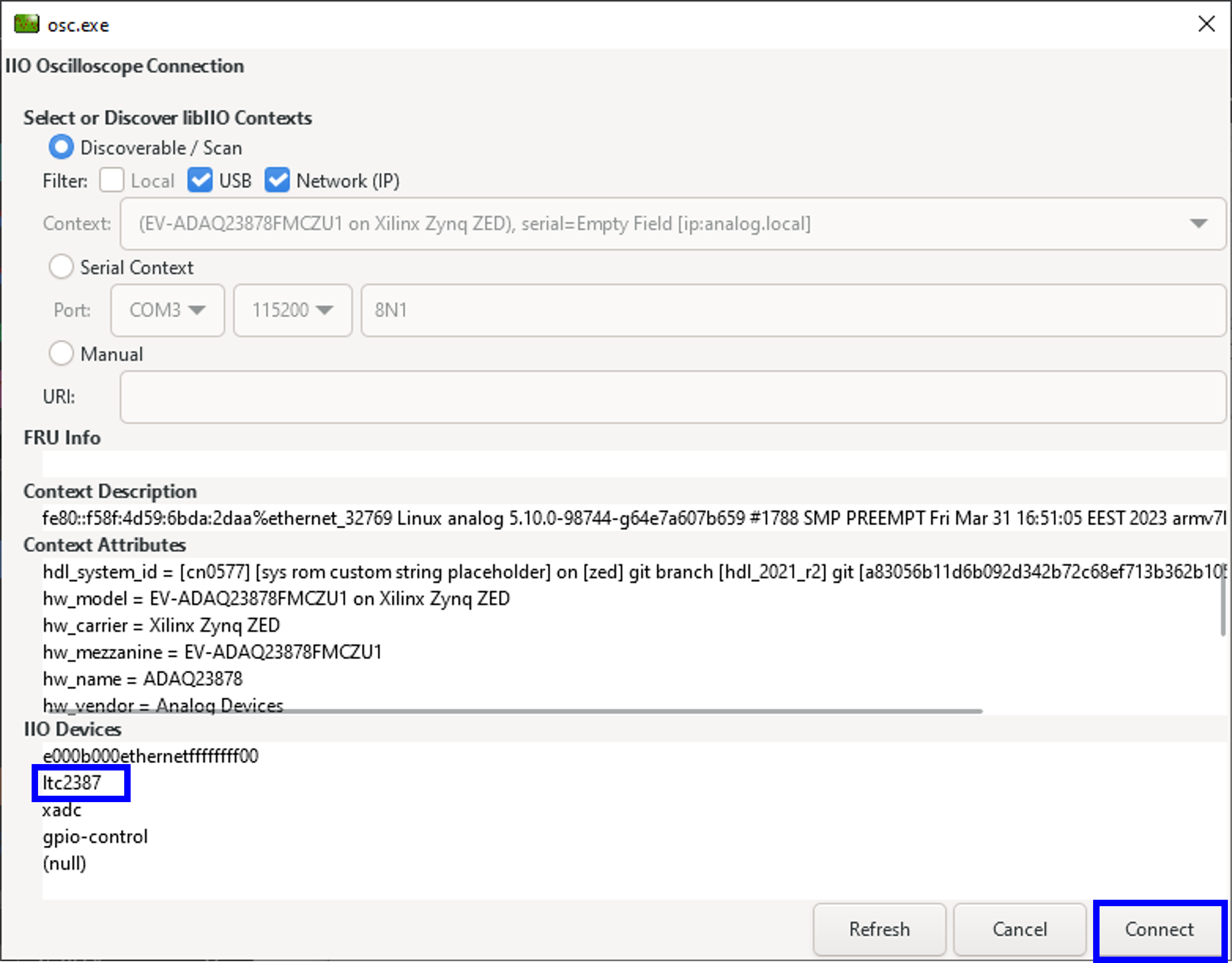
IIO Oscilloscope Capture Window
Waveform Plot:
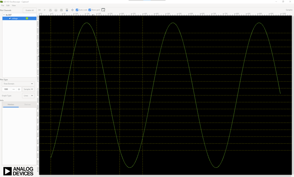
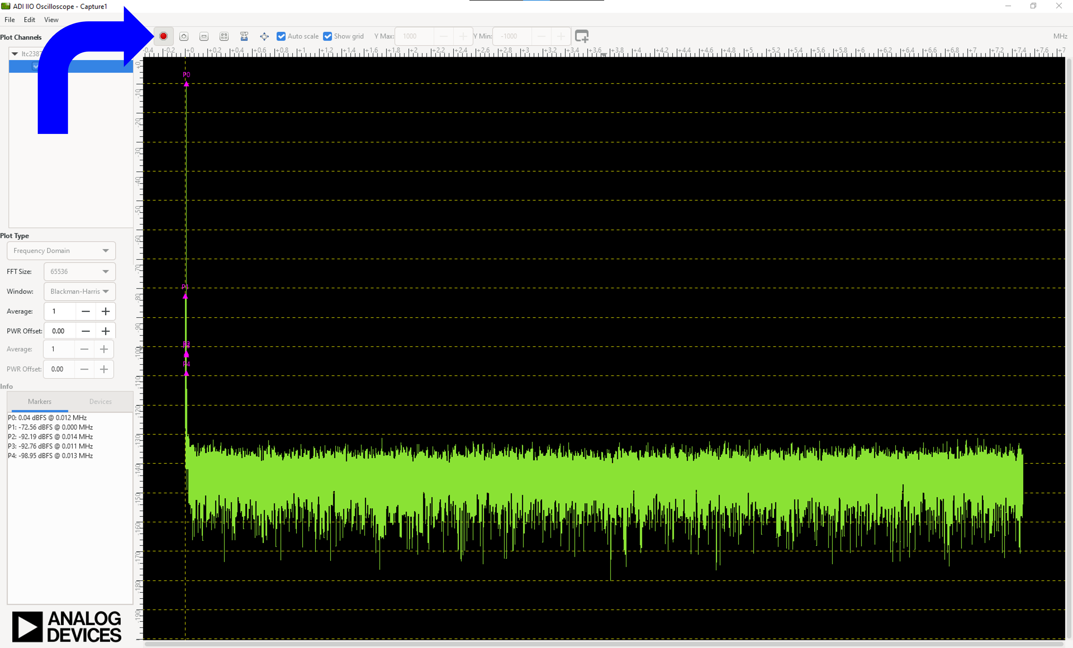
FFT Plot:
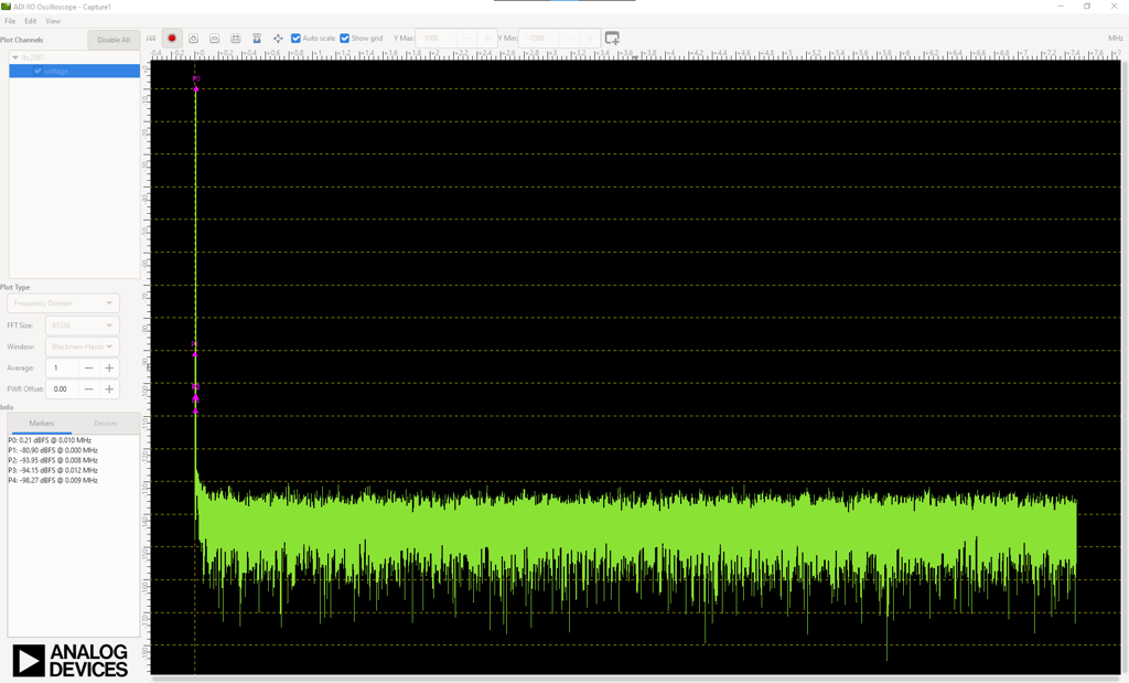
To obtain the FFT plot:
Select Frequency Domain for the plot type.
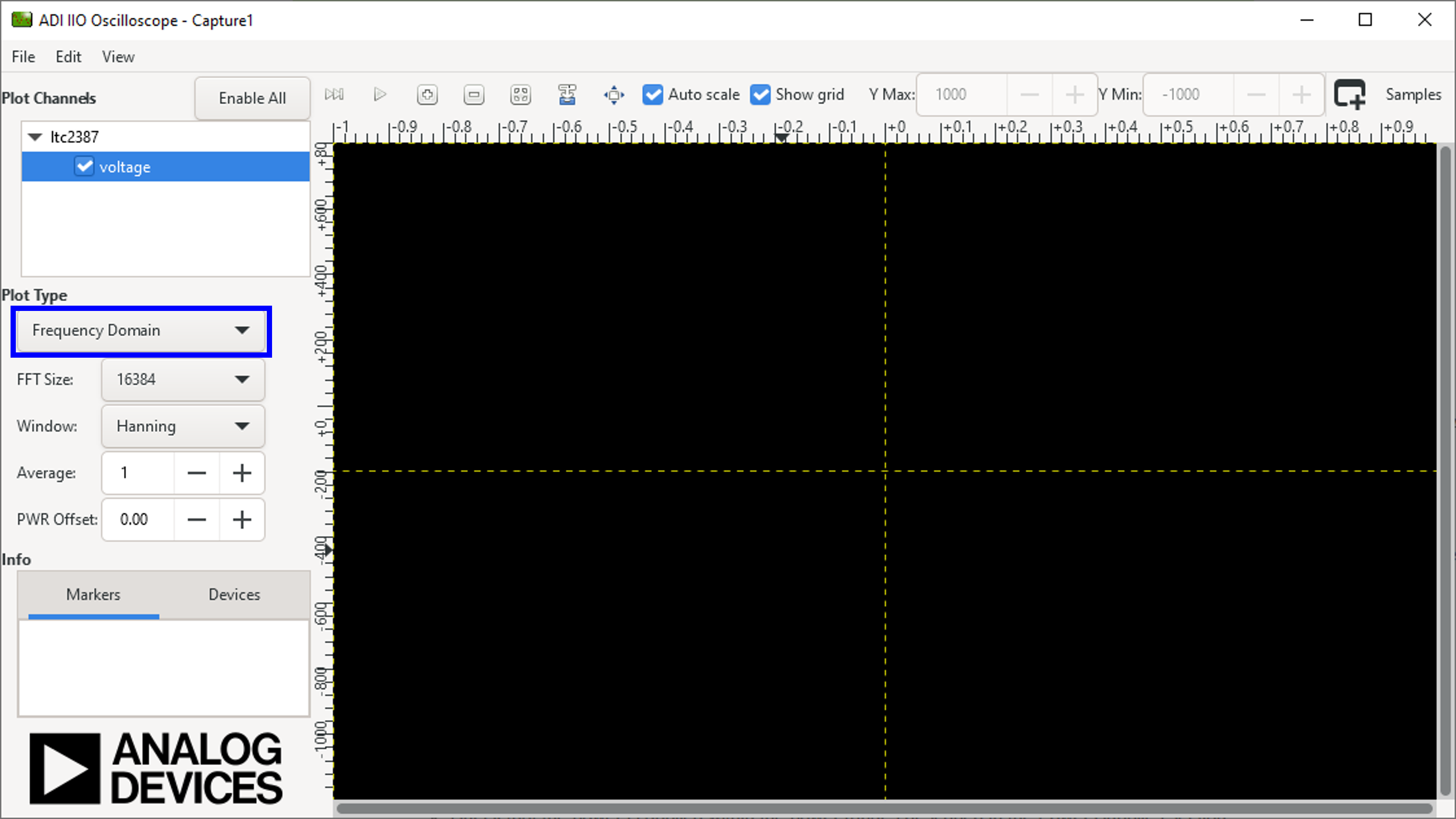
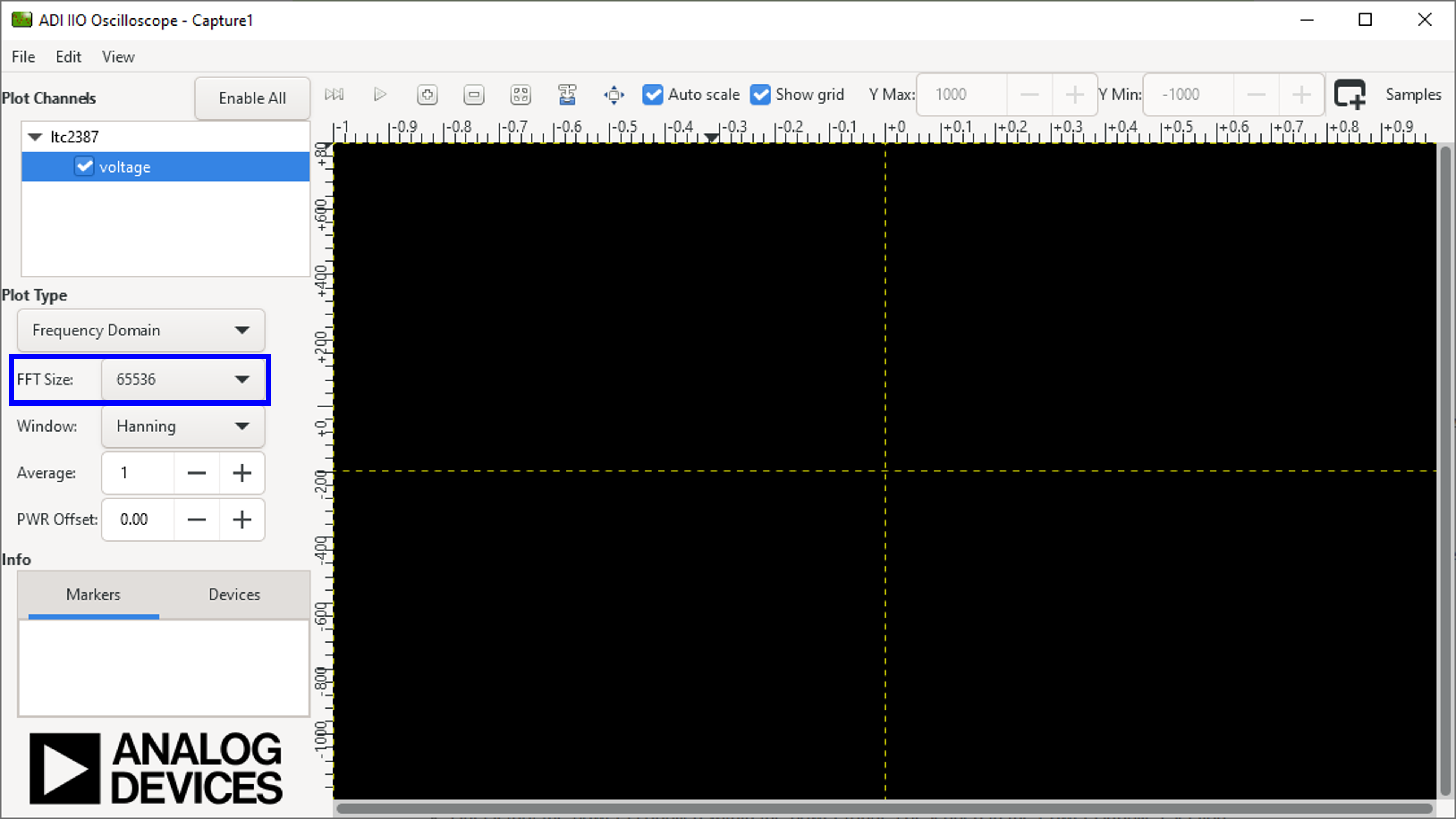
Designate the preferred number of samples under FFT size.
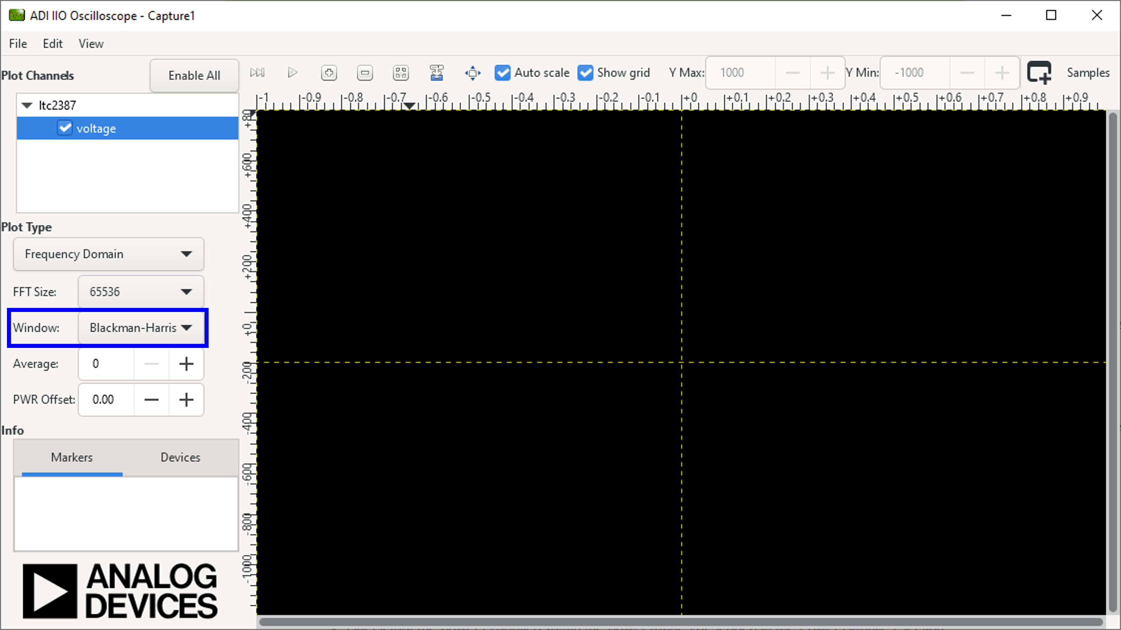
Specify the window type as Blackmann-Harris.
Press Run to view the result.
Board Layout Guidelines
PCB layout is critical for preserving signal integrity and achieving the expected performance from the ADAQ23876/ADAQ23878.
Use a multilayer board with an internal, clean ground plane in the first layer beneath the ADAQ23876/ADAQ23878.
Apply careful placement of individual components and routing of signals.
Route input and output signals symmetrically.
Solder the ground pins of the ADAQ23876/ADAQ23878 directly to the ground plane using multiple vias.
Remove ground and power planes under the analog input/output and digital input/output pins (including F1 and F2) to avoid undesired parasitic capacitance. Undesired parasitic capacitance impacts distortion and linearity performance.
Signal routing:
The pinout of the ADAQ23876/ADAQ23878 eases layout by placing analog signals on the left side and digital signals on the right side.
Separate sensitive analog and digital sections on the PCB.
Keep power supply circuitry away from the analog signal path.
Fast switching signals (CNV±, CLK±) and DA±, DB± digital outputs must not run near or cross analog signal paths.
Decoupling:
Use good-quality ceramic bypass capacitors of at least 2.2 µF (0402, X5R) at the output of each LDO regulator generating the µModule supply rails (VDD, VIO, VS+, VS−) to GND.
This minimizes electromagnetic interference (EMI) susceptibility and reduces glitch effects on the power supply lines.
All other required bypass capacitors are laid out within the ADAQ23876/ADAQ23878.
External decoupling capacitors on the REFIN, VDD, and VIO pins near the µModule can be removed with no significant impact on performance.
Mechanical Stress
Mechanical stress from mounting the device to the board can cause subtle changes to SNR and the internal voltage reference.
The recommended soldering method is IR reflow or convection soldering with a controlled temperature profile. Hand soldering with a heat gun or soldering iron is not recommended.
Board Schematic and PCB Layout
The complete design support package — including schematics, PCB layout, Bill of Materials, and Allegro project files — is available for download from the EVAL-ADAQ23876FMCZ and EVAL-ADAQ23878FMCZ product pages.