Activity: The Wien Bridge Oscillator
Objective
The objective of this exercise is to explore, understand, simulate, and finally construct a basic Wien bridge oscillator. As an added bonus, we will then build and test an alternate circuit with considerably lower distortion, approaching that of quality benchtop audio signal generators.
Design files for a printed circuit board version of this experiment are available so you can build one of your own as you follow the exercise.
A complete video run-through of the experiment, including circuit construction, testing, and measurements, is available in the video “A Low-Distortion Wien Bridge Oscillator You Can Build!”:
Background
The Wien bridge oscillator holds a significant place in electronics history. Hewlett Packard’s (HP) very first product, the model 200A audio signal generator, was based on Bill Hewlett’s 1939 master’s thesis at Stanford University. This groundbreaking device boasted impressive specifications for its time, including a 1 W output and distortion better than 1% over most of the audio range, powered by standard line voltage. Beyond testing telephone amplifiers and general audio circuits, one of its earliest and most notable applications was in the production of Disney’s Fantasia movie. You can even find a replica of Hewlett Packard’s original garage, complete with a model 200A, at Stanford University, commemorating its role as the birthplace of Silicon Valley’s “garage startup” culture. A link to a copy of Bill Hewlett’s original Master’s thesis is available for perusal in the Further Reading section, offering a fascinating glimpse into the circuit theory and design from that era. Another insightful reference is Linear Technology Application Note 43, Appendix C, “The Wien Bridge and Mr. Hewlett”.
What is an Oscillator?
Oscillators are circuits that generate periodic waveforms without requiring any input signal. They generally include some form of electronic amplifier stage — transistors, op amps, or vacuum tubes — with a frequency-selective feedback network consisting of a combination of passive devices such as resistors, capacitors, or inductors. The generality of this statement reflects the diversity of oscillator designs; there are plenty of other ways to make an electronic (or electric) oscillator. For example, the General Radio Type 213-B uses a mechanical tuning fork as the frequency selective component, and a carbon microphone as the amplification stage (See The General Radio Experimenter, Volume IV, number II) Regardless of the implementation details, in order to oscillate, a linear circuit must satisfy the Barkhausen stability criteria [1] , which in simple terms states that at the frequency of oscillation:
The loop gain is equal to unity in absolute magnitude
The phase shift around the loop is zero or an integer multiple of 2π
Consider the first requirement, and its consequences in an oscillator: If the loop gain is less than unity, the oscillations will die out. If the loop gain is greater than unity, the oscillations will increase in amplitude, either forever (which is possible in a simulation), or until something limits the amplitude (hopefully gracefully, and not as the result of a catastrophic failure.) If the end application is not very sensitive to distortion (output frequencies at multiples of the desired fundamental frequency), then simple gain limiting methods can be employed - this could be as simple as allowing the amplifier output to “clip” at the supply rails. But if the application requires a pure sine wave, then carefully controlling the amplifier’s gain is absolutely critical.
Consider the second requirement; there are various feedback elements employed to generate the required frequency-dependent phase shift — quartz crystals, mechanical resonators, L-C (inductor-capacitor) networks, or - R-C (resistor-capacitor) networks, including the Wien bridge.
The Wien Bridge
The Wien bridge was developed by Max Wien in 1891, as an extension of the Wheatstone bridge. Whereas the Wheatstone bridge consists of purely resistive elements, the Wien bridge can be used to measure capacitors. While initially intended as a measurement circuit, at balance, the phase shift of a Wien bridge is zero, so including a gain element with a phase shift of zero will satisfy one part of the Barkhausen criterion.
(It would have been impossible, or at least exceedingly difficult, to make an oscillator based on the Wien bridge in 1891 as no linear electronic gain elements existed — the audion tube was invented in 1906.)
There are several advantages to using a Wien bridge as the feedback element in an oscillator:
Simplicity
Low distortion
- Ease of frequency adjustment, via either:
variable resistors
variable capacitors
A Fully Operational “Classic” Wien Bridge Oscillator
With the gain and phase shift requirements satisfied, the next step is to ensure a loop gain of exactly unity. At resonance, the reactive arm of the Wien bridge has an attenuation of 1/3, so the amplifier must have a gain of 3. The circuit shown in Figure 1 is a simple Wien bridge oscillator with a 1.0 kHz output that illustrates this principle.
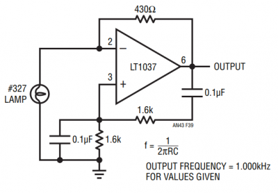
Gain control is achieved with an incandescent light bulb (as it is in Bill Hewlett’s configuration.) An incandescent bulb’s resistance increases with power dissipation, and as a rough rule of thumb the hot resistance is often about 10 times the cold resistance. The #327 lamp shown has an operating voltage of 28 V and operating current of 40 mA, for a hot resistance of about 700 Ω and a cold resistance of around 70 Ω, which matches the actual measurements of a few bulbs. To achieve a noninverting gain of 3, the lamp’s resistance must be half of the feedback resistance, or about 215 Ω.
Once the circuit is oscillating, the amplitude control can be intuitively understood as:
If the gain is a bit less than 3, the lamp cools down, its resistance drops, tending to increase the gain.
If the gain is higher than 3, the lamp heats up, its resistance increases, tending to reduce the gain.
Eventually, the gain settles to a value that is likely very close to 3 — whatever is required to maintain oscillation — and the amplitude stabilizes. Now we have a practical circuit.
Simulation of a Wien Bridge Oscillator with Ideal Elements
Before working with real components and all of their imperfections, a useful exercise is to “build” a few conceptual circuits in LTspice, just to get a taste of what life would be like in an ideal world. The LTspice files can be downloaded here: Wien Bridge Active Learning Exercise LTspice files.
LTspice can be downloaded for free at the LTspice Product Page.
Wheatstone Bridge Simulation
In order to become familiar with the operation of a bridge circuit in general, open the wheatstone_bridge.asc simulation in LTspice and run it. The output should be similar to Figure 2.
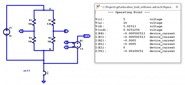
Note that the bridge is initially unbalanced, and a small, but nonzero voltage appears at Vcd. (A Voltage-controlled voltage source with a gain of unity is a convenient way to measure the difference between two nodes such that it appears directly in the simulation results.) Experiment with different values for R3, noting that a value of 10 kΩ should balance the bridge and give a zero output. Try reducing R1 and R2 to 1 kΩ — does this have any effect on the output voltage?
AC Wien Bridge Simulation
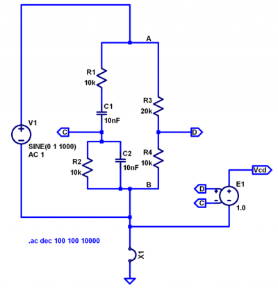
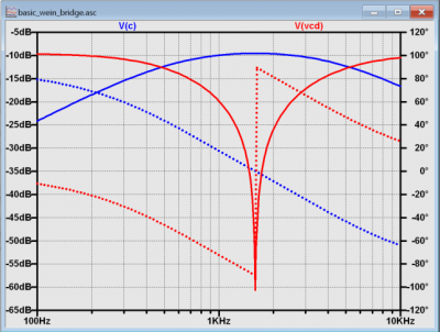
Let’s explore the operation of the Wien bridge, which has frequency dependent elements. Open the basic_wein_bridge.asc simulation in LTspice, shown in Figure 3. The simulation is set up as an AC sweep from 100 Hz to 10 kHz, with the result shown in Figure 4. Note that a DC bridge supply would produce a fairly obvious output; after an initial transient, node C would settle to ground potential, and node D would be at 1/3 of the supply. Run the simulation and probe node C, the output of the reactive arm of the bridge. Notice the gentle hump in response, peaking somewhere slightly less than 2 kHz. Probe node Vcd next. Notice the extremely sharp null in response, making it very easy to locate the exact resonant frequency of 1.59 kHz.
Simulated Wien Bridge Oscillator
Now let’s amplify the bridge’s output and pipe it back to the input. Open the wien_bridge_vcvs_gain.asc LTspice simulation shown in Figure 5. This is a circuit that is impossible to build in real life—the gain stage is essentially perfect: infinite input impedance, zero output impedance, and no offset or gain error. But it allows us to experiment with ideal cases, to gain some intuition into the Barkhausen criterion and test out some assertions made in the background information.
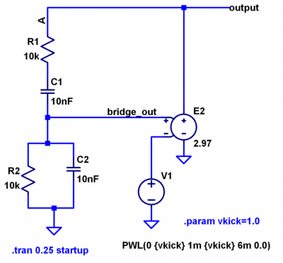
Ignoring V1 for the moment, note that when this simulation is started, all voltages are zero. There is no reason for it to do anything other than stay at zero forever. V1 is there to “kick” the circuit into operation by providing a step to the gain stage when the simulation is first started, then it ramps back to zero and has no further effect on the circuit’s operation. Run the simulation, and probe the output node. Results should look similar to Figure 6.
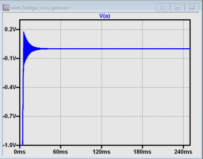
Note that the circuit oscillates for a few milliseconds, but the amplitude exponentially decays to zero. This is because the gain is set 1% too low (as you might expect if you built an amplifier with 1% resistors and got unlucky in the low gain direction). Next, set the value for E2 to 2.997, or about 0.1% too low, as shown in Figure 7. Oscillations continue longer, but still decay.
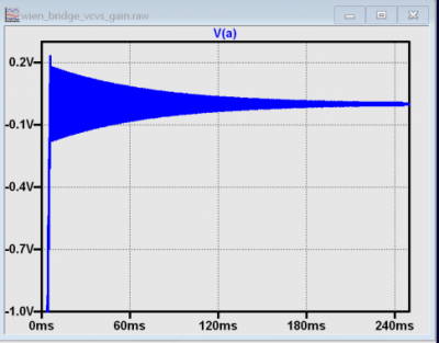
Since we know that the gain needs to be exactly 3 to sustain oscillation, set the gain to 3.0 as shown in Figure 8 and run the simulation.
Notice that the operation is exactly as predicted, with a steady amplitude for the entire 250 ms simulation time. Such behavior is purely theoretical and wouldn’t occur in real-world circuits or realistic simulations using a model of a real amplifier; the finite open-loop gain, finite input impedance, offset, and other imperfections will always cause the gain to be slightly more or less than 3.
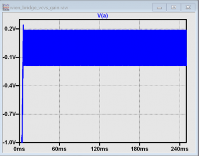
As a final illustration that simulations can model situations that would be impossible in the real world, set the gain to 3.03 (1% too high, as you might expect if you built an amplifier with 1% resistors and got unlucky in the high-gain direction), as shown in Figure 9, and run the simulation.
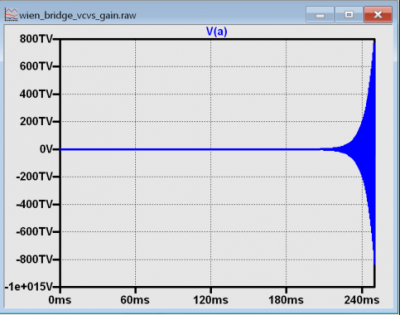
The output amplitude hits 800 teravolts after 250 ms, with no end in sight. Again, this simulation is only to build intuition about the Barkhausen criterion and has no basis in reality. If you were to build this circuit with an op amp configured with a gain of 3.03 and powered by ±5 V, oscillations would build until they approached 5 V amplitude, then simply clip (producing a distorted waveform).
Simulation and Construction of a Complete, Practical Wien Bridge Oscillator
We’ve informally discussed using a light bulb as a gain control element. While this does work, you can’t just choose any old light bulb and expect the circuit to operate properly, the bulb must be chosen carefully. Let’s first explore a practical implementation using antiparallel diodes to “gently” control the amplifier’s gain.
Materials
ADALM2000 (M2K) Active Learning module OR:
Two-channel oscilloscope, signal generator, and/or network analyzer functionality
±5 V bipolar tracking power supply
ADALP2000 Parts Kit Items:
Solderless Breadboard
Jumper Wire Kit
2 - 10nF Capacitor
2 - 1 µF Capacitor
3 - 10 kΩ Resistor
2 - 4.7 kΩ Resistor
1 - 5 kΩ Single-turn potentiometer
2 - 1N4148 Silicon Diode
Alternatively, printed circuit board files with matching LTspice simulations are available to fabricate a PCB version of this experiment, available at Wien Bridge PCB files and LTspice files.
The circuit shown in Figure 10 is a complete (and practical) Wien bridge oscillator circuit that can be built on a breadboard. Rather than using an incandescent bulb (which has a positive coefficient of resistance) for the amplifier’s input resistor, this circuit shunts part of the feedback resistance with diodes, which have a negative coefficient of resistance. Ignoring the diodes, the gain would be 1+(10k+4.7k)/(4.7k+2k)), or about 3.19. But as the voltage across D1 and D2 approaches 600 mV or so, the effective resistance of R2 is reduced, dropping the gain.
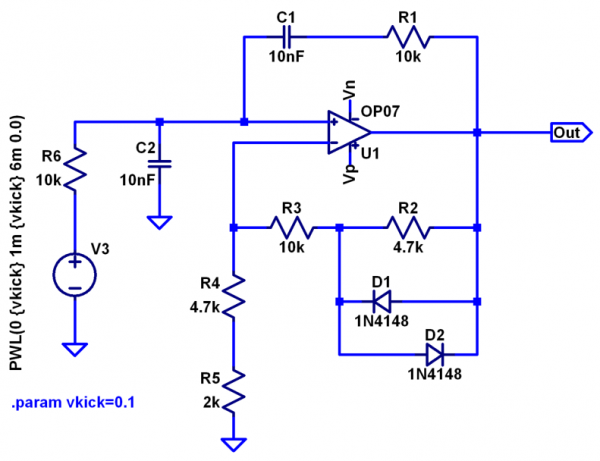
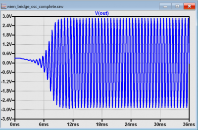
Open wien_bridge_osc_complete.asc in LTspice, and run the simulation; the output should resemble Figure 11. The “kick” circuit is not actually necessary to get the simulation to start; it will start… eventually. But the amplifier’s offset in the model is quite low, so the kick helps the simulation start up much faster. Startup time is also a concern in some real-world applications, and circuits similar to V3, such as a pulse generator made from logic gates can be employed. Experiment with different values for vkick (including zero).
Next, construct the circuit as shown in Figure 12.
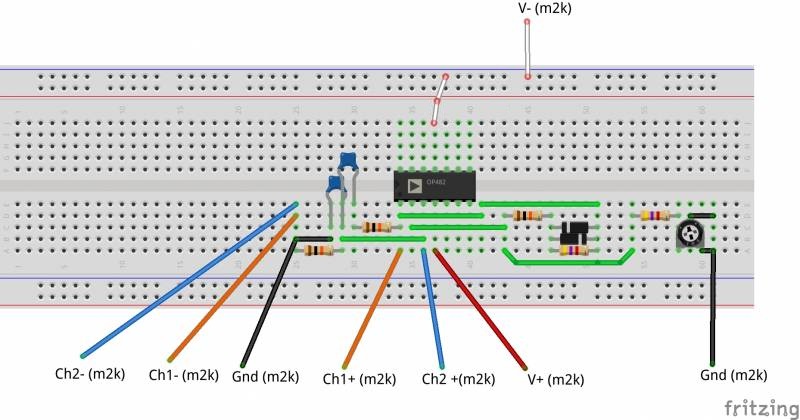
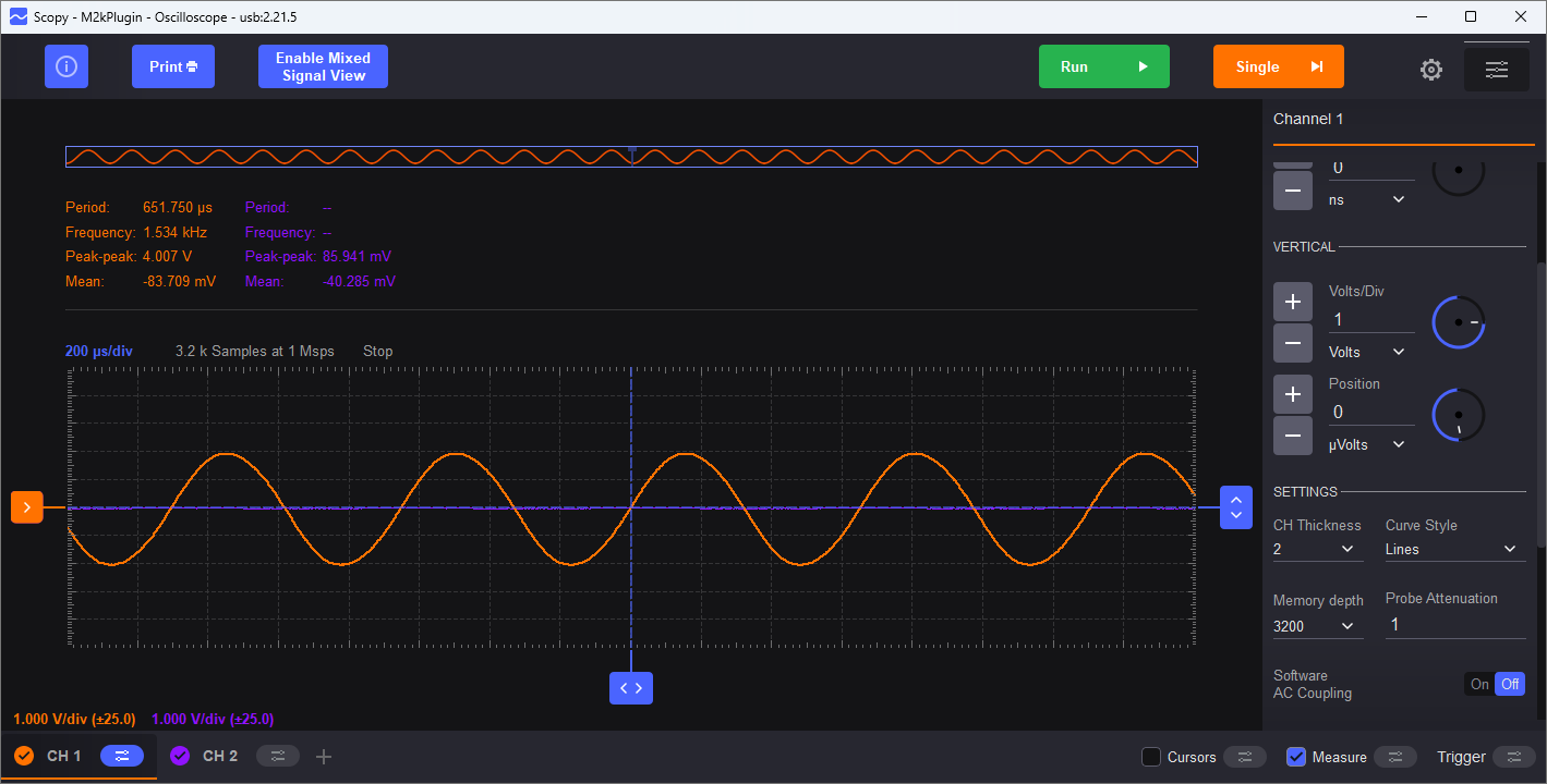
Note that R5 is a potentiometer, allowing the gain of the circuit to be “dialed in” to where oscillation just starts. Measure the output with Scopy’s oscilloscope; set the vertical to 1 Volts/Div and the timebase to 200 µs/Div. The results should be similar to Figure 13.
That is a “pretty nice” looking sinewave, but how nice is it? Can your eye detect any distortion at all? It is nearly impossible to visually detect distortion in a time-domain (oscilloscope) plot - even with a perfect reference sinewave to compare against, distortion less than 1% is difficult to see. To truly analyze low-level distortion components, Fourier Transform techniques are required, and that is exactly what Scopy’s spectrum analyzer does. Open up the spectrum analyzer, and set the start frequency to 0 kHz, Stop frequency to 20 kHz, Top to 0 dB, and Bottom to -120 dB. IMPORTANT: Click the channel 1 settings, select Blackman-Harris window, and set the Gain Mode to High.
Note
The ADALM2000 has two input ranges, ±2.5 V and ±25 V. These are selected automatically in the oscilloscope as you adjust the vertical gain, but not in the spectrum analyzer. If you increase the oscillator’s gain to the point where the output exceeds ±2.5 V, you will need to set the Gain Mode to Low to avoid clipping, which will not damage anything but will result in excessive distortion.
Observe the spectrum of the oscillator’s output, as in Figure 14.
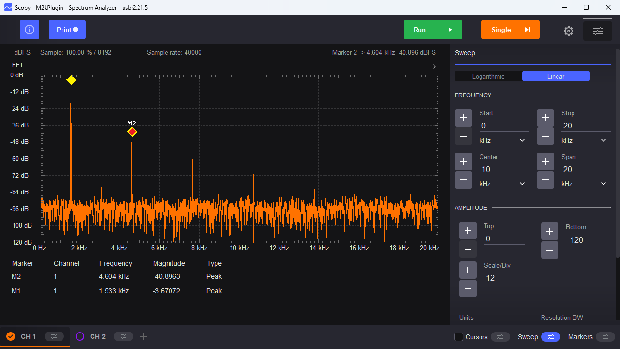
While the diode clamp method of limiting the gain is simple, it’s difficult to get better than approximately -40 dB (about 1%) distortion.
Questions
What is the relationship between the gain control elements and distortion?
What would happen to the distortion components (harmonics) if you replaced one of the diodes in the diode clamp circuit with a Schottky diode, which has a lower forward drop than a silicon diode?
A Much Lower Distortion Version of the Circuit
Let’s build up a variant of the circuit shown in Figure 1. The #327 incandescent bulb is a 28 V indicator lamp with a cold resistance of approximately 130 Ω and a hot resistance of approximately 650 Ω. This can be modeled as a resistor in LTspice, with resistance being a function of the power dissipation. But the resistance can’t change instantaneously—if it did, then as the output sine wave went from zero, to full-amplitude, back to zero, and to full negative amplitude, the amplifier’s gain would change in concert, distorting the output waveform; this is NOT what we are after.
The operation of the circuit relies on the bulb’s thermal time constant being much longer than half the output period. Why half the output period? Recall that the formula for power dissipated in a resistor is V²/r, so both positive and negative output swings produce positive power dissipation. This time lag is modeled by translating the bulb’s power dissipation into a current, which drives a parallel R-C network (R100 and C100), with a resulting time constant of 50 ms—much longer than the 628 μs half-period of the 1.59 kHz output. Thus the bulb’s resistance is dependent on the average power dissipation over many cycles.
Open the wien_bridge_osc_experimenter.asc simulation, shown in Figure 15. Note that this simulation file is in the PCB design files folder.
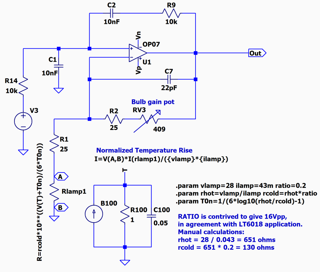
Figure 15 LTspice Simulation of Incandescent Bulb Amplitude Control
Run the simulation and probe the output, as shown in Figure 16.
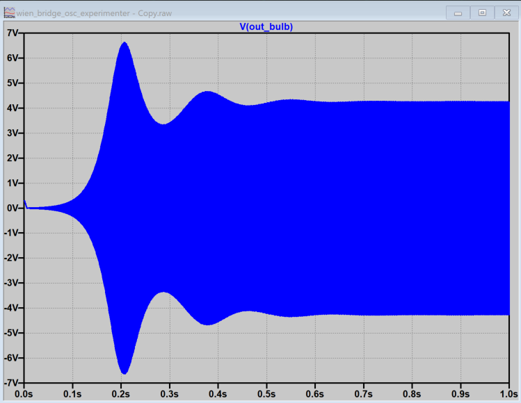
Figure 16 Output from an LTspice simulation of incandescent bulb amplitude control
Note the initial transient, where the circuit is “hunting” for just the right amplitude to sustain oscillation. While this circuit may be built up on a breadboard, if you have made it this far into the exercise, you might want to have something a bit more reliable and permanent. Figure 17 shows the completed PCB with the ADALM2000 connected.
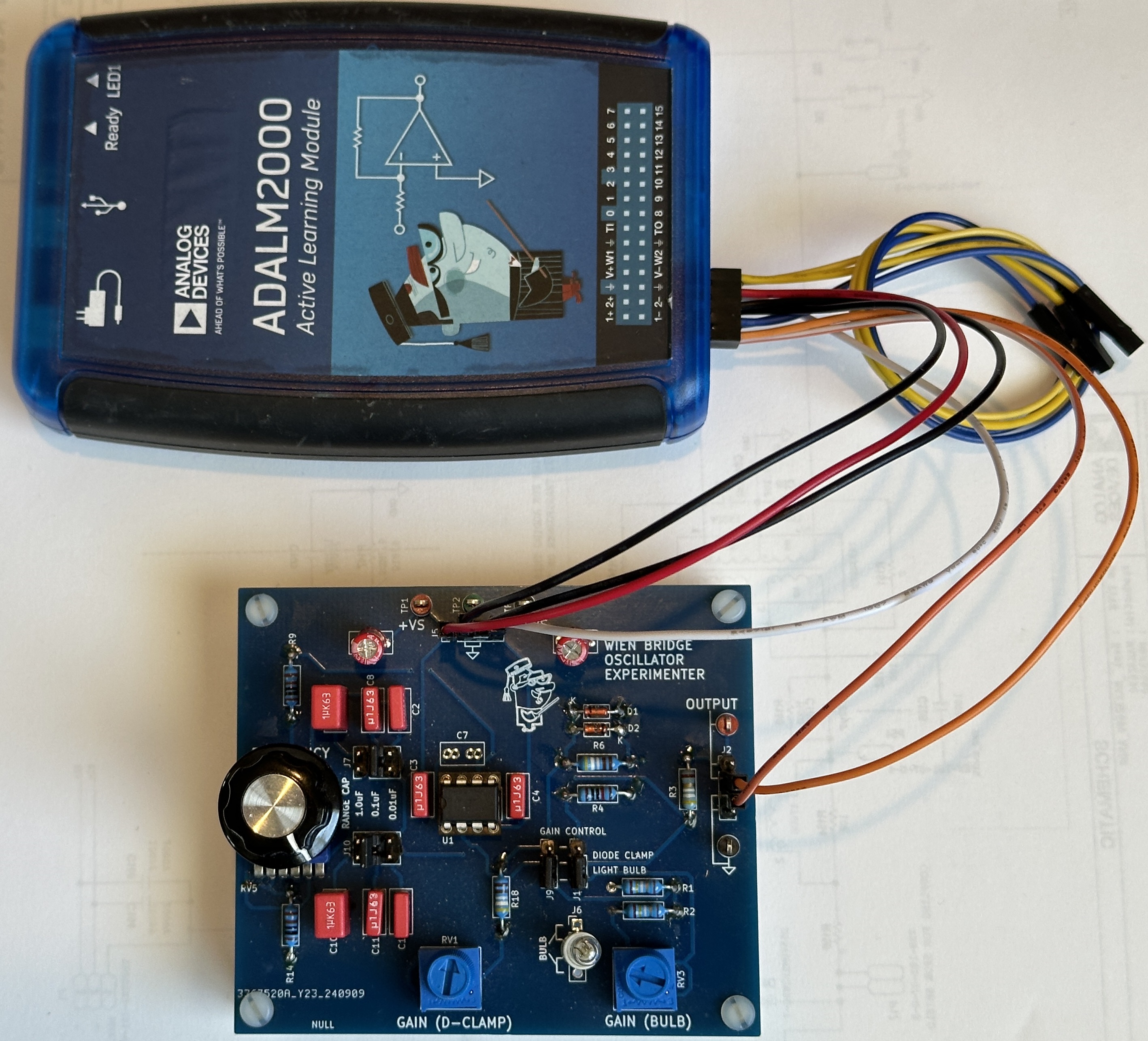
Figure 17 Assembled Wien Bridge Oscillator Experimenter Board
Figure 18 shows the output spectrum of the Wien bridge oscillator experimenter board set to bulb control. Note that the third harmonic is better than –60 dB, or 0.01% — 10 times lower than typically achievable with the diode-clamp circuit. In fact, this is pushing the distortion floor of the ADALM2000 itself! While the exact number varies, there’s an axiom that a measurement instrument should be 4 to 10 times better than the device under test. We have reached the limit of the ADALM2000; the only option for confidently measuring this circuit’s distortion is to use a better test instrument.
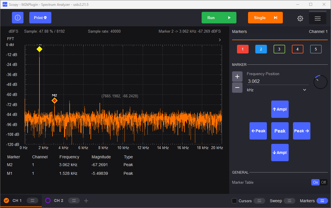
Figure 18 Output Spectrum, Incandescent Bulb Amplitude Control
Questions
What is the state of the art for distortion measurement instruments in the audio range?
If you can’t afford a state of the art benchtop distortion analyzer, are there other options?
(Hint: Watch the video at the start of this article!)
Further Reading
Acknowledgements
This exercise was inspired by an ASEE 2022 conference workshop presented in partnership with Dr. Robert Bowman, author of the book “EE Freshman Practicum”. The full workshop video is available here:
Resources
Footnotes
Warning
All the products described on this page include ESD (electrostatic discharge) sensitive devices. Electrostatic charges as high as 4000V readily accumulate on the human body or test equipment and can discharge without detection. Although the boards feature ESD protection circuitry, permanent damage may occur on devices subjected to high-energy electrostatic discharges. Therefore, proper ESD precautions are recommended to avoid performance degradation or loss of functionality. This includes removing static charge on external equipment, cables, or antennas before connecting to the device.