User guide
Hardware guide
Hardware configuration
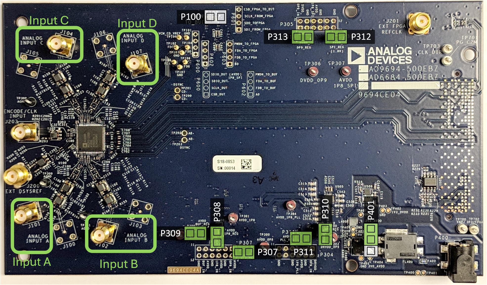
Connector layout
Tip
For more information on Sysref, see the JESD204B Survival Guide.
Jumper configuration
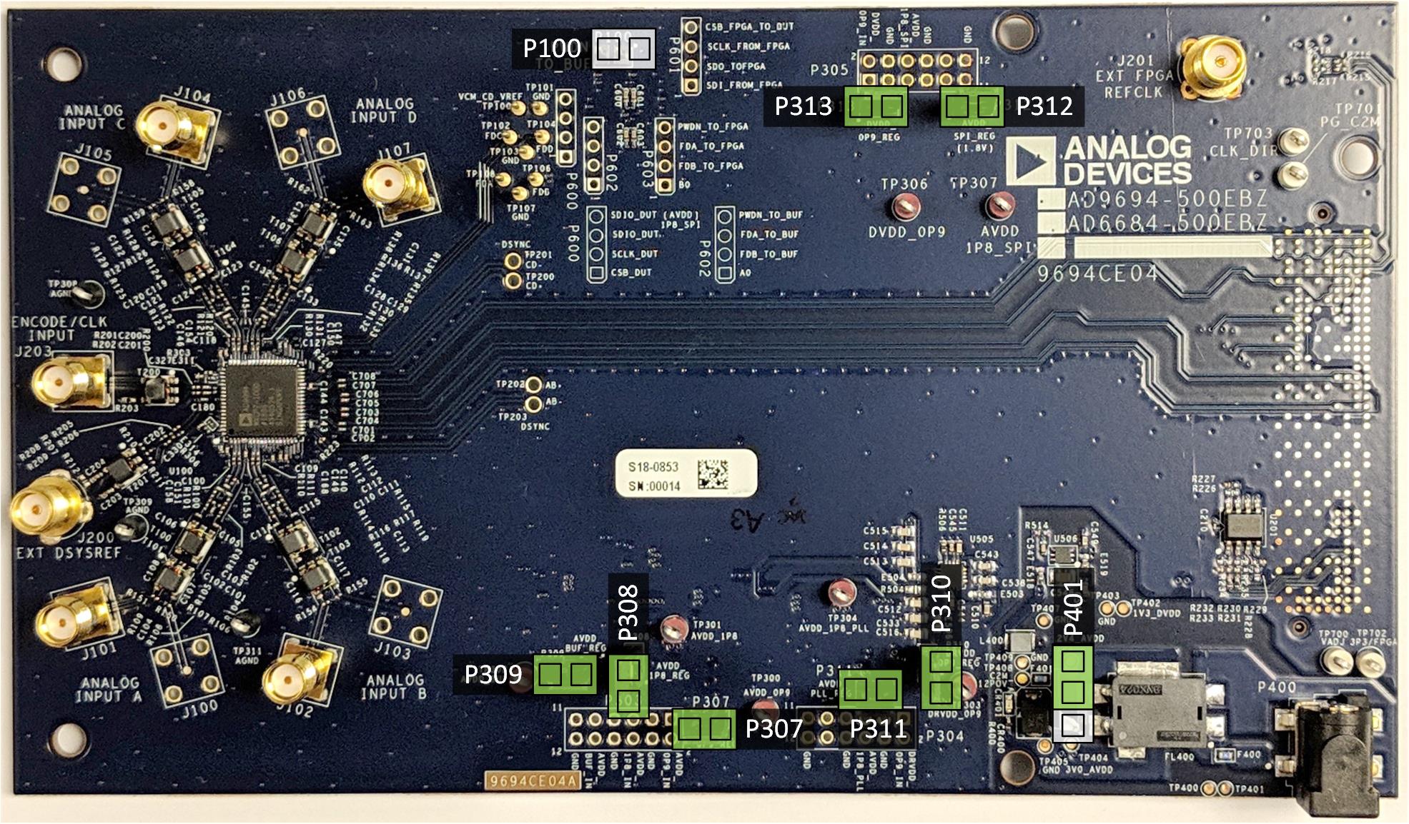
Before using the evaluation board, configure the jumpers as highlighted in green in the evaluation board figure. Refer to the ad9694-500ebz legacy page for detailed jumper positions for both old and new board revisions.
Power supply
The AD9694-500EBZ can be powered externally or through the FMC connector from the FPGA carrier board. It supports 12 V-1 A and 3.3 V-3 A supplies from FMC. The evaluation board VADJ range is 1.2 V to 2.5 V.
Warning
Removing jumpers or the board while powered via FMC may damage the board and/or chip. Always power down before making changes.
Analog inputs
The AD9694 has four analog input channels organized as two pairs:
J101 — Channel A input
J102 — Channel B input
J104 — Channel C input
J107 — Channel D input
Connect a clean, low-jitter signal source to the desired channel via coaxial cable. It is recommended to use a narrow-band band-pass filter with 50 Ohm terminations.
For the ADC sample clock, connect a low-jitter clock source to connector J203 (up to 1 GHz, 50 Ohm coaxial cable, 14 dBm).
Schematic, PCB Layout, Bill of Materials
Design and integration files (schematic, PCB layout, BOM) are available from the AD9694 product page under the Design Resources tab.
Helpful documents:
AN-835 Application Note, Understanding ADC Testing and Evaluation
Software guide
The AD9694-500EBZ is supported through the Libiio library on ADI Kuiper Linux, which runs on the FPGA carrier board (ZCU102). Applications that interface via libiio include:
IIO Oscilloscope — graphical waveform and spectrum analyzer
Analog Devices Hardware Python Interfaces — Python interface
For a step-by-step walkthrough, see the ZCU102 Quickstart guide.