User guide
The complete user guide of the evaluation board can be found at EVAL-AD4884 User Guide.
Hardware guide
Input stage
The input stage for each AD4884 channel consists of a pair of LT6236 op amps. The LT6236 is selected for its wideband (90 MHz), low noise, favorable distortion performance and low power consumption. The op amps are set up as unity-gain buffers, ensuring that a preceding signal source or sensor is presented with a high impedance. With supply rail values of +5 V and -5 V, the valid range at each input of this stage is -3 V to +3.7 V.
The input stage is designed to take in a fully-differential signal. With a differential voltage span of +/-2.91 V, the full span of the ADC is exercised. A single-ended signal can also be applied at the input, but modifications such as adding gain or a bias level to one of the op amps might be needed to exercise the full span of the ADC.
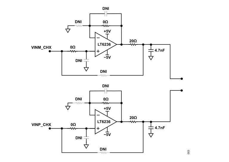
The following can be configured in the input stage:
Stage bandwidth
Additional band limiting through RC input filter and/or capacitors across amplifier feedback
Stage gain (unity gain by default, non-inverting gain setting available)
Stage bypass (no bypass by default, bypass via amplifier mezzanine card is an option for Channel A only)
Gain configuration
By default, the EVAL-AD488X-FMC is configured with a gain of 1.03x, and 220 pF capacitors fitted for noise filtering across the feedback network of the AD4884 on-chip FDAs. In this default configuration, an SNR of around 91.9 dB is typically expected.
Changing the gain at the AD4884 FDA stage requires light rework on the PCB (removing or adding 0402 SMD resistors and/or shorting 0402 solder pads). For the possible gain options and node shorting requirements, refer to the AD4884 data sheet.
Voltage reference
The AD4884 requires an external 3 V voltage reference. The ADC includes an internal reference buffer and capacitor, which simplifies reference selection and eliminates the need for an external buffer.
The following references are available on the evaluation board:
Power supply
The EVAL-AD488X-FMC is designed to operate from the 12 V and 3.3 V supplies provided from the host controller board via the FMC connector. The FMC supplies are regulated down using a combination of switching regulators and low dropout (LDO) regulators to generate the necessary power rails for the on-board circuitry.
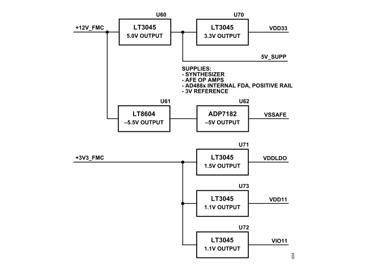
ADC power supplies
The AD4884 requires three major power supplies:
VDD33: 3.3 V analog supply rail
VDD11: 1.1 V ADC core supply
IOVDD: 1.1 V digital interface supply
The 1.1 V rails can be sourced from:
On-board LT3045 LDO regulators (default)
Internal AD4884 LDO regulator
Off-board external supply
The 3.3 V rail can be sourced from:
On-board LT3045 LDO regulator (default)
Off-board external supply
Amplifier power supplies
A +5 V rail (VDDAFE) and a -5 V rail (VSSAFE) are generated on the evaluation board. These rails power all analog front-end circuitry, which includes the four LT6236 discrete operational amplifiers in the input stage as well as the on-chip fully differential amplifiers inside the AD4884 (via the +VS and -VS pins).
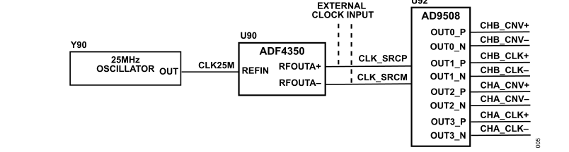
Clock generation
The EVAL-AD488X-FMC contains the necessary circuits to generate low jitter data (CLK+/CLK-) and conversion (CNV+/CNV-) clocks across the full operating range of the AD4884.
The circuit consists of:
The synthesizer takes in the 25 MHz signal and produces a higher frequency output with a programmable multiplication factor. The output is then fed to the clock buffer, which generates the CLK and CNV signals with separate programmable frequency division factors.
Digital interface
The EVAL-AD488X-FMC utilizes the FMC connector from the ZedBoard to support ADC device configuration via 4-wire SPI, conversion result access using the LVDS interface, and conversion control in LVDS mode.
The AD4884 operates with a 1.1 V digital interface supply voltage. To translate between this 1.1 V level and the digital interface voltage level of the ZedBoard (VADJ), SN74AVC1T45DCKR bidirectional level translators are used on the evaluation board.
Schematic, PCB layout, bill of materials
Description |
Download |
|---|---|
Design files (schematics, PCB layout, bill of materials) |
Software guide
The EVAL-AD488X-FMC hardware is controlled and configured through the ACE Software. ACE is a desktop software application that allows the evaluation and control of multiple evaluation systems. The controller board supported by ACE with the EVAL-AD488X-FMC is the ZedBoard.
The evaluation board is also supported with the Libiio library. This library is cross-platform (Windows, Linux, Mac) with language bindings for C, C#, Python, and others. Applications that can be used with it are:
ADI IIO Oscilloscope
The IIO Oscilloscope is a cross-platform application for interfacing with IIO devices, enabling you to configure device parameters and visualize data.
Important
Make sure to download/update to the latest version of IIO Oscilloscope.
For Linux
Remote run on host
The IIO Oscilloscope application can be used to connect to another platform that has a connected device, to configure the device and read data from it. This application is not for performance testing, but rather showcasing the basic features.
Please see IIO Oscilloscope documentation for installation steps and more details.
Build and start osc on a network-enabled Linux host.
For Windows computers, open the application from the start menu.
Once the application is launched, go to Settings > Connect > URI and type “ip:” then the IP address of the target in the pop-up window. This IP can be found out with a command from the previous section of this documentation.
Scopy
Scopy is a cross-platform software toolbox for interfacing with ADI devices, enabling you to configure device parameters, visualize data, and perform advanced signal analysis.