

System Architecture
Every HDL design of a reference project can be divided into two subsystems:
Base design - contains an embedded processor (soft or hard) and all the peripheral IPs that the carrier board supports.
Board design - direct integration of all the necessary IPs used to support an FMC I/O board.
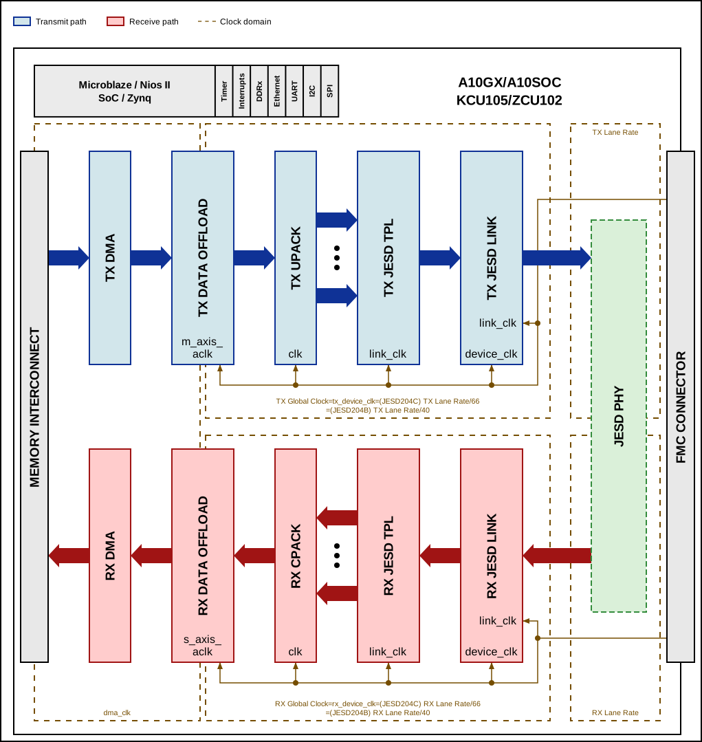
DAQ2 Hardware Architecture
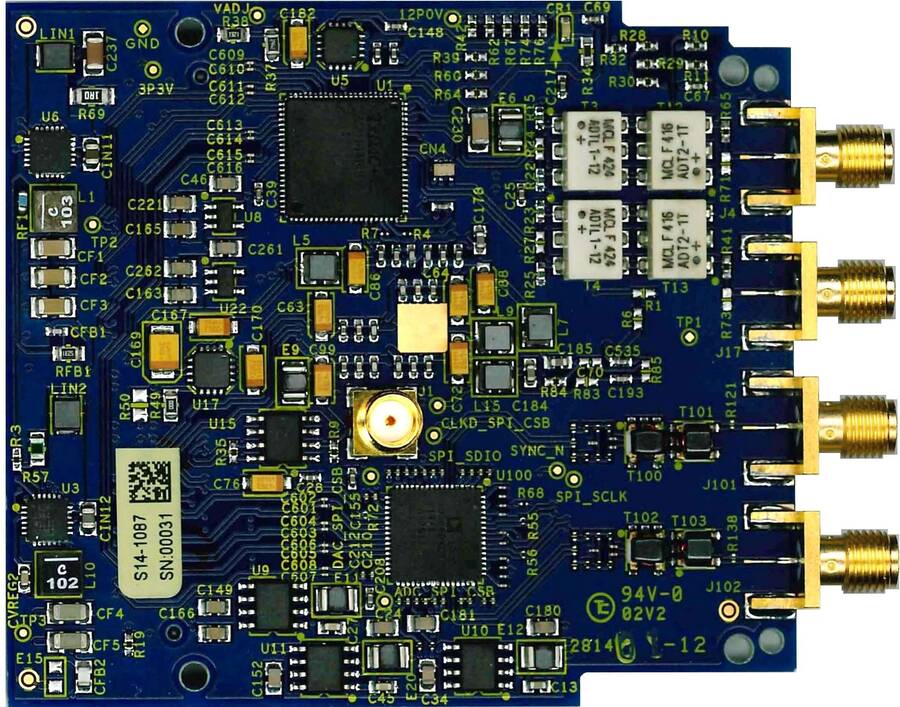
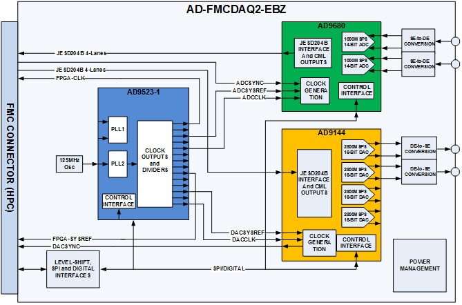
The AD-FMCDAQ2-EBZ module is used here as an example to illustrate how a JESD204B-based system is structured. The module comprises:
AD9680 dual, 14-bit, 1.0 GSPS, JESD204B ADC
AD9144 quad, 16-bit, 2.8 GSPS, JESD204B DAC
AD9523-1 low jitter clock generator
The hardware can be divided into four functional partitions: transmit path, receive path, clocking, and control/power management.
Transmit Path
The reference design generates digital signals for the AD9144 using the JESD204B interface. The physical layer consists of 4 lanes running at 10 Gbps. The device is configured and controlled via SPI and directly active GPIO signals.
Receive Path
The reference design captures data from the AD9680 using the JESD204B interface. The physical layer consists of 4 lanes running at 10 Gbps. The device is configured and controlled via SPI and directly active GPIO signals.
Clocking
The clocking architecture uses a 125 MHz onboard crystal as input to the AD9523-1. The clock generator upconverts this to approximately 3 GHz using an internal VCO, with an integer multiplier of 24x producing 3000 MHz.
The VCO output is then divided to provide:
1000 MHz sample clocks for both the DAC and ADC
500 MHz reference clocks for the FPGA transceivers
SYSREF signal for deterministic latency (Subclass 1)
The AD9523-1 provides a clean, low-jitter clock distribution network that is essential for achieving optimal JESD204B link performance.
References
DAQ2 HDL Project - AD-FMCDAQ2-EBZ HDL reference design
Generic JESD204 block designs - Generic JESD204 block designs
JESD204 Interface Framework - JESD204 Interface Framework