ADRV2CRR-FMC Carrier Board Hardware Overview
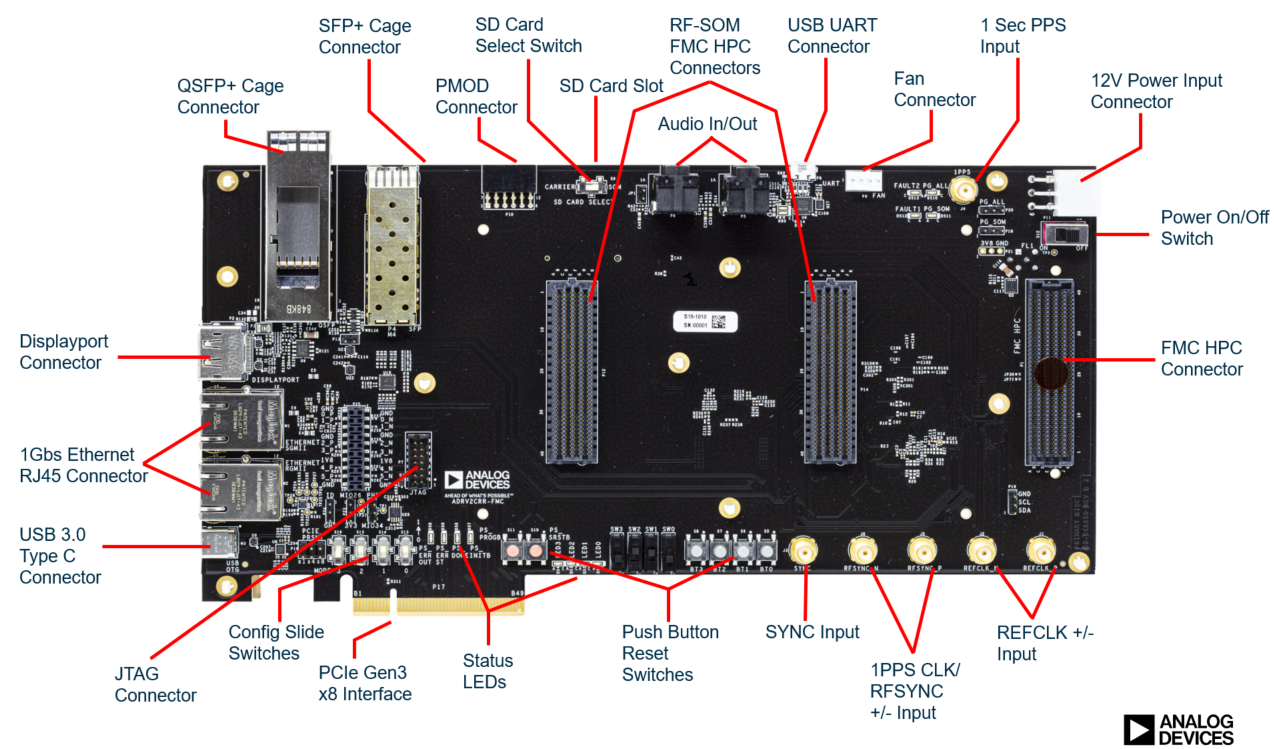
The ADRV2CRR-FMC is the carrier board to allow users evaluate the functionality of the ADRV9009-ZU11EG RF-SOM. It contains common high speed I/O ports to give flexibility in what connectivity option the user needs. It comes with a power supply that powers up the full system, heatsink that the user fits to the RFSOM heat spreader plate and necessary cables and adapters to get up and running.
Information on getting started and links to access the system software provided is contained on the main RF-SOM page.
Power Input
The ADRV2CRR-FMC has a single 12V supply input, distributed to the internal power supplies and interface connectors. Included in the package is a 12V, 145W power supply, which powers the complete prototyping platform built out of ADRV9009-ZU11EG, ADRV2CRR-FMC and AD-FMCOMMS8-EBZ. There are four LEDs that show the status of the power supplies: PG_ALL, PG_SOM, PWR_FAULT1 and PWR_FAULT2. A detailed description of these signals is available in the ADRV9009-ZU11EG RF-SOM Hardware Overview page.
ZU11EG Ultrascale+ Configuration
Boot Mode Pins
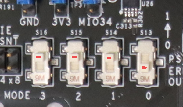
Slide switches (S13 - S16) select the boot source of the Xilinx ZU11EG Ultrascale+.
Mode Pins [3:0] 0000 JTAG
Mode Pins [3:0] 0010 Quad-SPI (32b)
Mode Pins [3:0] 1110 SD1 (3.0)
SD Card
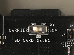
SD card selection S9 switches between carrier and SOM SD card connector
JTAG
The JTAG connector P7 is a 2x14 pin header intended to fit the Xilinx Platform Cable.
RF-SOM Interface Connectors
The interface to the ADRV9009-ZU11EG consists of two SAMTEC SEARAY™ 400-pin connectors (P12 and P14). For a detailed description of the signal interface visit the ADRV9009-ZU11EG RF-SOM Hardware Overview page.
FMC Connector
The ADRV2CRR-FMC includes a standard ANSI/VITA 57.1 FMC high-pin count connector P1, which is partially populated. Following signals are present:
10 serial transceiver lanes FMC_HPC_DPx, 2x serial transceiver reference clock FMC_HPC_GBTCLKx
34 differential IO pairs FMC_HPC_LAx, 2 differential clocks FMC_HPC_CLK0/1_M2C
JTAG, I2C interfaces
FMC HA and HB differential signals are not populated with user-defined digital IOs as specified in the FMC HPC standard. Instead, RF reference clock signals, synchronization signal, and ADRV9009 IOs are connected to these positions to enhance the capability of the P1 connector by providing the possibility:
to add extra ADRV9009 transceivers to the system, and synchronize these with the RF-SOM. This is accomplished with the AD-FMCOMMS8-EBZ
to design custom RF boards that make use of the analog and digital ADRV9009 IOs.
Important
All the previous mentioned ADRV9009 IOs, and reference clocks are connected to P1 through 0 Ohm jumpers (JP8-JP91). If an FMC mezzanine card is connected, which conflicts with these signals remove the 0 Ohm jumpers. For the synchronization signal SYNC_OUT2 remove R21
IO Expansion Connector
IO expansion connector P25 is a 2.54mm pitch 2x10mm female connector that gives access to 12 single-ended (6 differential pairs) general purpose IOs, connected to high-performance ZU11EG PL bank 65. The expansion IOs are referenced to 1.8V. If other levels are needed voltage level translators need to be used.
PMOD Connector
PMOD connector P10, is a 2x6 pin, low-speed host interface, referenced to 3.3V.
Important
Fairchild FXLA108 bidirectional voltage level translator is used on the PMOD signals, to connect these to the 1.8V referenced ZU11EG PL banks. The FXLA108 has auto direction sensing, and might not work properly with some signals, like bidirectional SPI data lines, or open-drain signals.
Interfaces
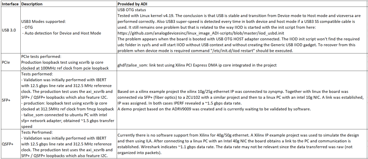
The following table outlines levels of functionality provided in software for the I/O interfaces on the carrier board.
Download
The Footprint is located here:
Revision Options
These are X-GRADE options.
Download
Download
Download
Download
Switches/Jumpers
USB PHY configuration (the only supported configuration)
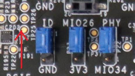
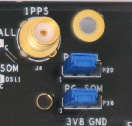
Power good jumpers (P18, P20) (the only working configuration)