ADRV9009-ZU11EG RF-SOM Hardware Overview
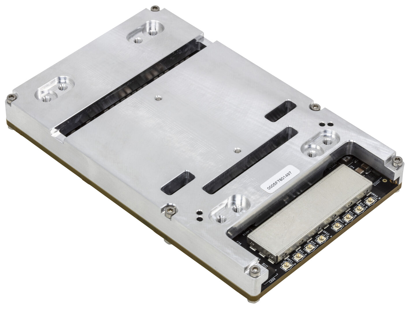
The ADRV9009-ZU11EG RF-SOM package includes:
ADRV9009-ZU11EG board with heat spreader plate mounted on top
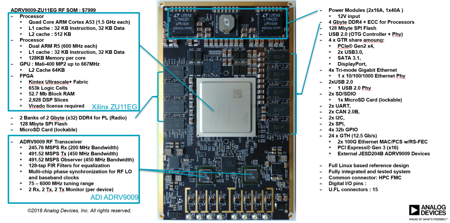
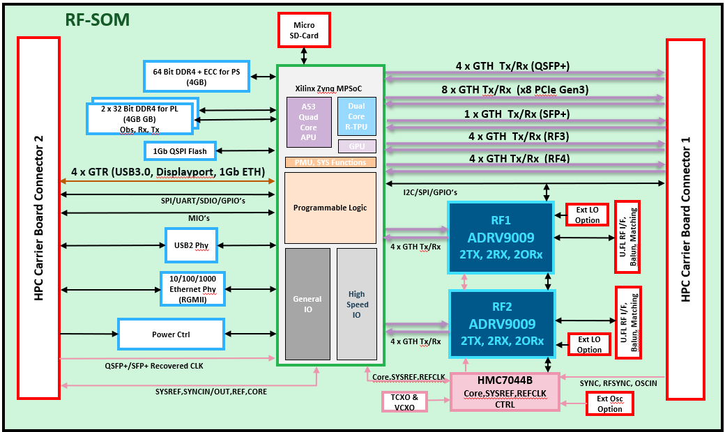
High level block diagram showing key components and IO routing
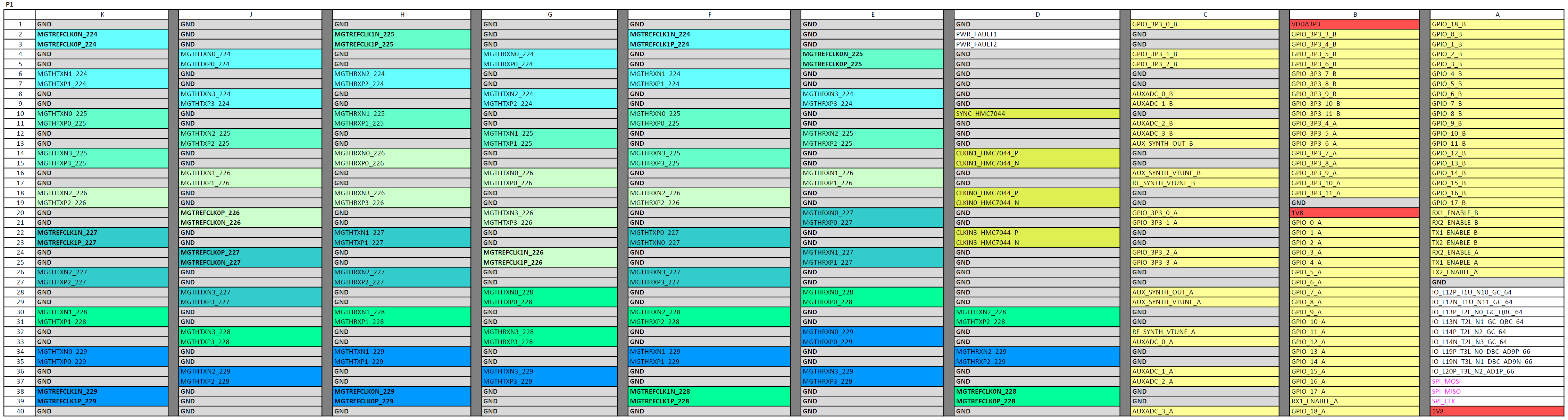
Connector Interface
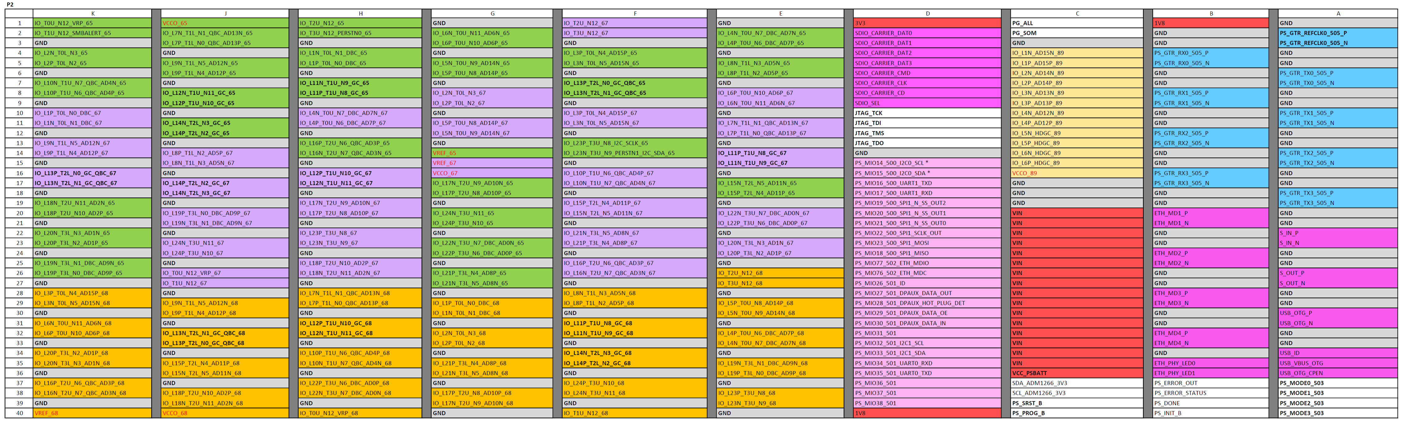
The interface of the ADRV9009-ZU11EG consists of two SAMTEC SEARAY™ 400-pin female connectors P1 and P2. Following signals are present:
P1 Connector:
24x GTH transceiver lanes MGTHTX_N/P, MGTHRXN/P; GTH Reference clock inputs MGTREFCLKN/P
Reference clock inputs for the on-board HMC7044B clock generator
Synchronization input signal for the on-board HMC7044B clock generator
Analog IO signals from the two on-board ADRV9009 transceivers GPIO_3P3_x, AUXADC_x, RF_SYNTH_VTUNE, AUX_SYNTH_OUT, AUX_SYNTH_VTUNE
Digital IO signals from the two on-board ADRV9009 transceivers GPIO_x, RX_Enable, TX_Enable. These signals are also connected internally to the ZU11EG PL.
Dedicated SPI bus for the two on-board ADRV9009 and HMC7044B
Xilinx Ultrascale+ ZU11EG programmable logic GPIOs
Power fault signals: PWR_FAULT1, PWR_FAULT2
1.8V digital supply output. Should be used only for powering IO buffers.
ADRV9009 auxiliary 3.3V voltage output VDDA3P3
P2 Connector:
ZU11EG programmable logic GPIOs
ZU11EG PS MIO pins
ZU11EG GTR lanes
SD 3.01 memory card interface, MDI interface to the on-board Marvell 88E1512 Ethernet PHY, USB 2.0 interface to the on-board Microchip USB3320C PHY
ZU11EG JTAG interface; dedicated configuration pins: mode pins, PS_DONE, PS_INIT_B, PS_ERROR_OUT, PS_ERROR_STATUS, reset signals
I2C interface for programming the on-board ADM1266 power sequencer
Power good signals: PG_SOM, PG_ALL
12 V power input
ZU11EG PL bank IO supply inputs VCCO_x, bank reference inputs VREF_x
1.8V, 3.3V digital supply outputs. Should be used only for powering IO buffers.
Download
A detailed description of the connector interface for the complete system ADRV9009-ZU11EG and ADRV2CRR-FMC is located here:
Power Input
The ADRV9009-ZU11EG is powered from a single 12V supply. Requirements for the supply are 12V +/-8%, 120W.
Hot Swap Controller
ADRV9009-ZU11EG features a hot-swap controller ADM1177 that allows safe board insertion from a live back-plane. ADM1177 also comes with digital current and voltage monitoring via on-chip 12-bit analog-to-digital converter communicating through I2C interface with the processor. ADM1177 is available in Linux as a hardware monitor device and could be accessed using python to measure SOM’s current consumption.
Download
Python script to read ADRV9009-ZU11EG RF-SOM power consumption:
Power Monitoring
The ADM1266 voltage sequencer/supervisor is used to handle following tasks:
Monitors 12V voltage input. If it exits the +/-4% (11.5V…12.5V) window PWR_FAULT2 signal will be asserted, if it exceeds +/-8% (11V…13V) the power to the RF-SOM will be switched off.
Controls the power-up voltage sequence of the internal supplies. Asserts PG_SOM and monitors the incoming PG_ALL signal.
Supervises internal voltage supplies during operation. If any of the internal supplies exceeds under/over voltage limits power to the RF-SOM will be turned off
Supervises on-board temperature. If the on-board temperature exceeds 65 °C PWR_FAULT1 signal will be asserted, if it passes 90 °C power to the RF-SOM will be switched off.
Turns power off in any of the previous mentioned cases, deasserts PG_SOM and records the event in a non-volatile Blackbox.
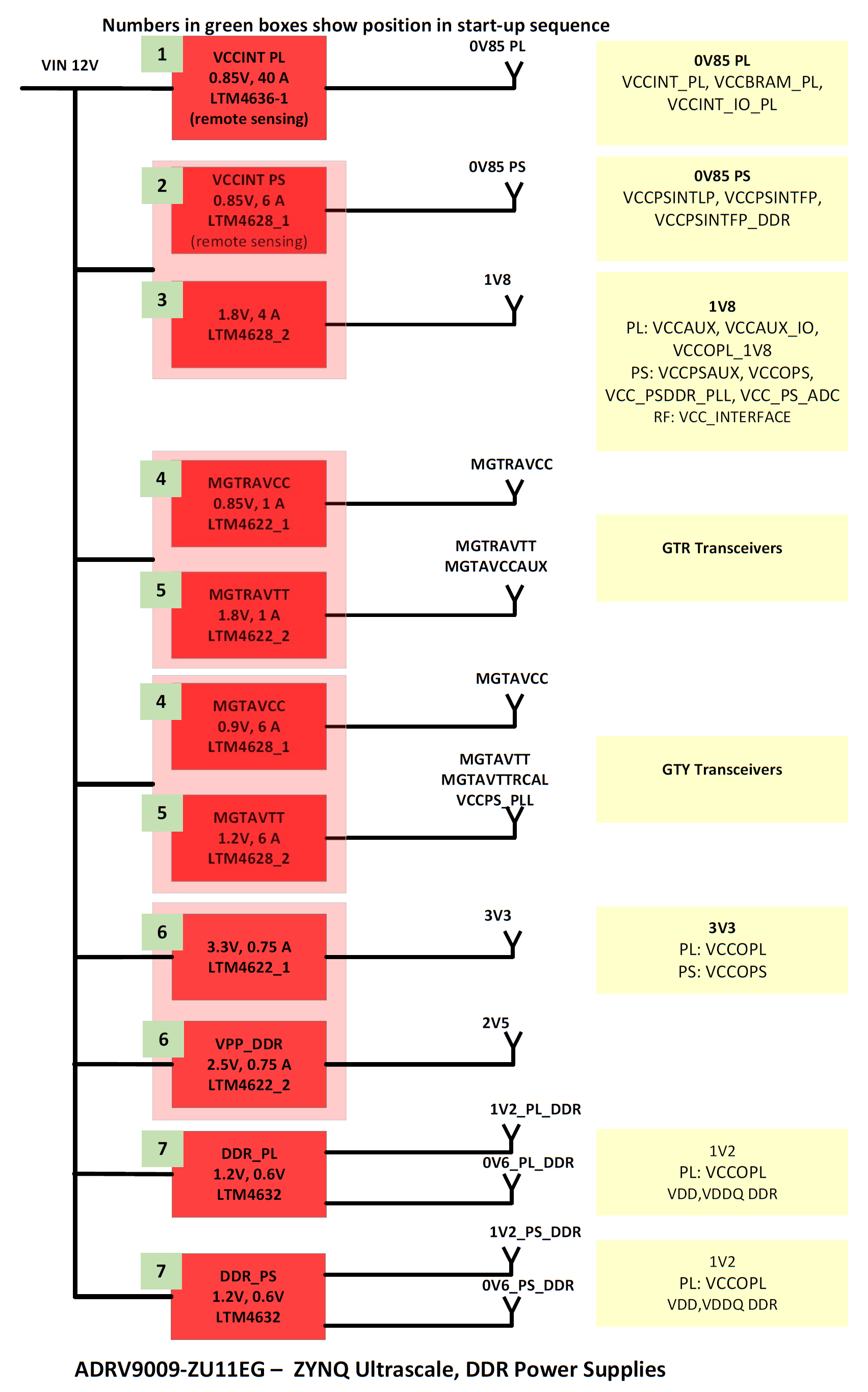
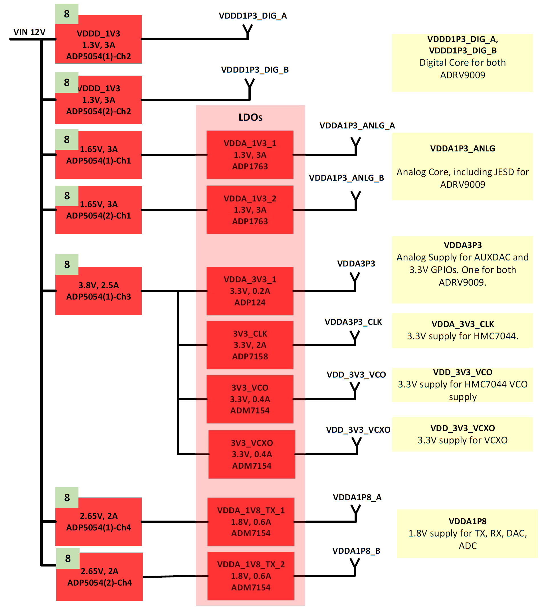
Power Tree
The diagrams below show the full power rail distribution for the ADRV9009-ZU11EG RF-SOM.
Power Fault Signals
The two fault signals PWR_FAULT1 and PWR_FAULT2 are open-drain active high signals with internal 4.7K pull-ups to 1.8V. These are controlled by the ADM1266 as previously mentioned. The purpose of the fault signals is to prompt that either temperature or input voltage are close to the limit, and a power down is imminent. Once power is turned off the state of the fault signals will reset, and the cause of the shutdown can be found only by accessing the ADM1266 Blackbox.
Power Good Signals
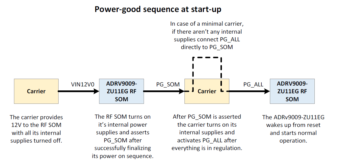
The RF-SOM uses the two power good signals, PG_SOM and PG_ALL, to ensure a correct power-up timing for the internal circuitry. While PG_SOM is an output controlled by the on-board ADM1266, PG_ALL is an input and must be asserted by the carrier. Both signals are active high open drain signals, with on-board pull-ups to 1.8V. The diagram below shows the power good sequence at start-up:
Reading the ADM1266 Blackbox Memory
Following tools are needed to read the Blackbox records:
ADI Power Studio GUI Software
EVAL-ADP-I2C-USB I2C USB dongle.
The I2C dongle connects to the ADM1266 dedicated I2C interface signals SCL_ADM1266_3V3, SDA_ADM1266_3V3 accessible in connector P2.
The image below shows how to connect the I2C USB dongle to P19 on the ADRV2CRR-FMC carrier board.
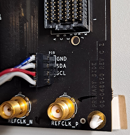
After connecting the I2C cable open the ADI Power Studio software, connect to the dongle and open the ADRV9009-ZU11EG RF-SOM project located below. The Blackbox Records can be accessed from the Monitor menu.
Download
ADRV9009-ZU11EG RF-SOM ADI Power Studio project:
Note
The .ssp file is an ADI Power Studio project file. Open it with
ADI Power Studio.
The System Power Map Diagram is located here:
Important
Troubleshooting power down issue on X-GRADE: EngineerZone
Interfaces
RGMII Ethernet
The RF-SOM has an on-board Marvell 88E1512 10/100/1000 Mbps Ethernet PHY connected to the GEM3 Controller in the PS on the Xilinx ZU11EG. The MDI signals are available in the interface connector P2.
USB
The ADRV9009-ZU11EG features both USB 2.0 and USB 3.0, configured in host, device or OTG mode. For USB 2.0 there is an on-board USB3320 ULPI transceiver connected to USB0 controller on the ZU11EG Zynq Ultrascale+. For USB3.0 the I/O path runs through the PS-GTR transceivers.
Gigabit Serial Interfaces
PS-GTR transceivers support data rates up to 6Gb/s and provide I/O path for USB3.0, SGMII Ethernet, DisplayPort.
GTH transceivers run up to 12.5Gb/s and being highly configurable, support a wide range of application like additional JESD lanes for synchronizing multiple ADRV9009 transceivers, 100Gb Ethernet, PCIe
Low Speed Interfaces
The PS Multiplexed IOs (MIO) give access to the low speed interfaces inside the Zynq Ultrascale+. The IO voltage level on all MIO pins is 1.8V. For other voltages external voltage level are required.
2x I2C buses. I2C0 is connected as well to the internal I2C bus and has 2.2K pull-ups to 1.8V.
1x SPI bus
2x UART buses. UART1 is used for debug messages and should be always connected.
Programmable Logic GPIOs
High Performance GPIOs
Programmable logic high performance banks 65, 67 and 68 are fully accessible in connector P2. Prior of using these signals the bank supply VCCO must be provided, with a voltage between 0.95V and 1.9V. A reference voltage must be applied as well, if the IO standard requires one. To use the internal VREF voltage a 500 or 1KOhm resistor needs to be connected from VREF pin to ground.
High Density GPIOs
Programmable logic High density bank 89 is partially available in connector P2. Connect a voltage between 1.14V and 3.4V to the bank supply voltage VCCO_89.
ADC inputs
Alternatively, some of the IOs in bank 89 AD12P/N to AD15P/N can be used as ADC inputs for the ZU11EG on-chip System Monitor. The internal 1.25V reference is used. The analog input range for unipolar operation is 0… 1V. For bipolar operation the differential voltage is between -0.5V … 0.5V, with the common-mode voltage 0.5V.
SD card
The ZU11EG on-chip SD Controller is compatible with SD memory card specification version 3.01, supporting UHS-I speeds and SDXC capacity format. The RF-SOM includes an on-board uSD card connector, but provides the possibility to place an SD card connector on the carrier. An on-board multiplexer is able to switch between the two connectors. SD IOs and SDIO_SEL signal are available in connector P2. Leave SDIO_SEL floating for uSD on RF-SOM. Pull SDIO_SEL to ground for using the SD on the carrier.
Minimal Carrier Setup
This chapter shows the connections to the ADRV9009-ZU11EG RF-SOM, that are mandatory for a minimum functional RF-SOM and carrier system.
Power Input and Power Good signals
Connect 12V, 120W voltage supply. Connect PG_ALL to PG_SOM.
Xilinx Zynq Ultrascale+ ZU11EG Configuration
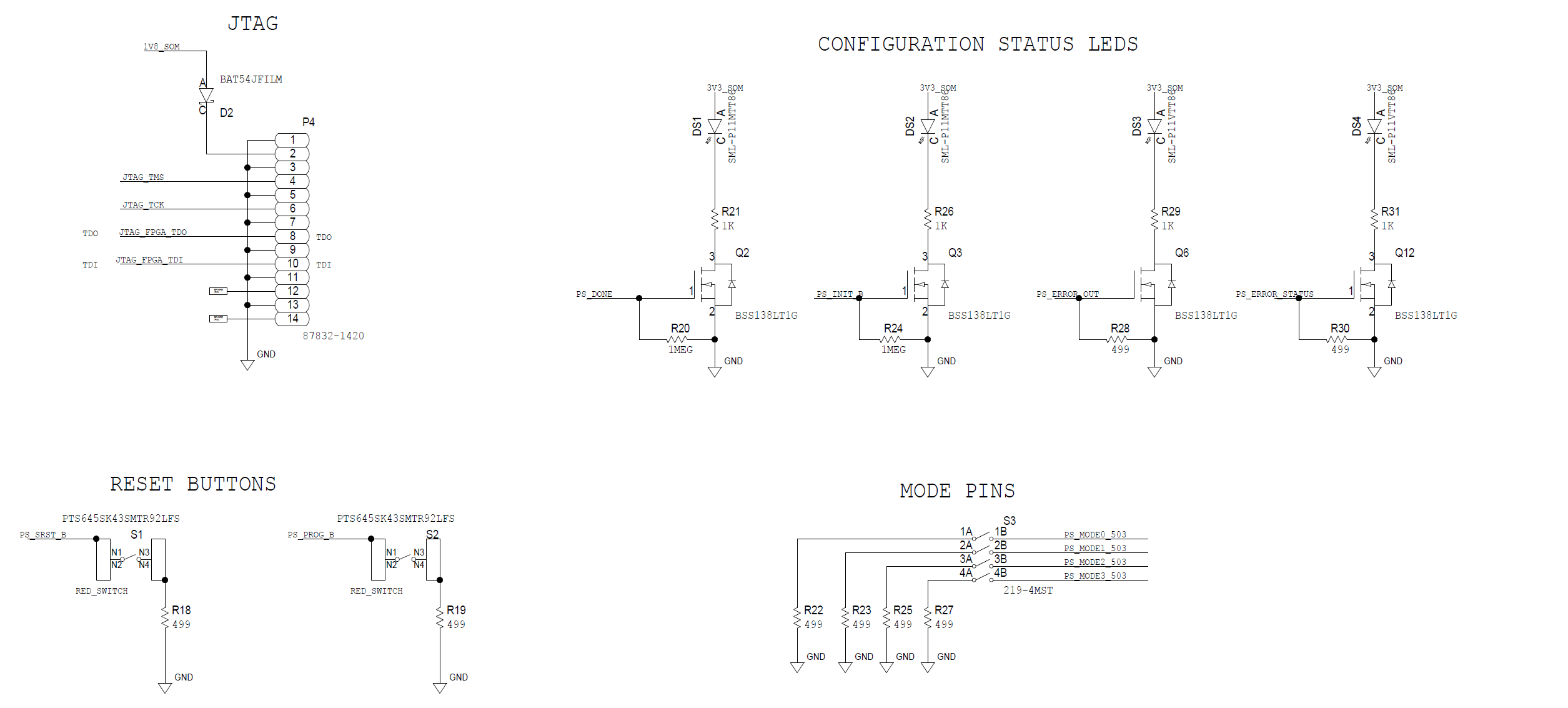
Reset Pins, Status LEDs, Mode Pins, JTAG connector
The carrier needs to include reset buttons, LEDs for status signals, slide switches for selecting the configuration mode and JTAG connector as shown here:
SD Card
If the mechanical setup requires, place an SD card on the carrier and pull SDIO_SEL to ground.
UART Interface for Debug
Connect UART1 interface in the carrier (MIO pins 16 and 17). The IO voltage level on these pins is 1.8V, so if a USB to UART interface like the FTDI FT232R is used, a voltage level translator from 3.3V to 1.8V must be used.
RGMII Ethernet
For a minimal setup it is recommended to use the RGMII Ethernet, since it requires only the RJ45 connector with magnetics on the carrier.
Clock and Synchronization Signal Inputs
Place BNC connector to provide access to input clock signals CLKIN0_HMC7044B_P/N, CLKIN1_HMC7044B_P/N and synchronization SYNC_HMC7044B. These signals are required for synchronizing multiple ADRV9009-ZU11EG RF-SOMs.
ADM1266 Power Sequencer I2C Interface
In order to be able to access the Blackbox memory the ADM1266 I2C interface needs to be accessible. Place a 1x4pin, 2.54mm pitch, male header to mate with the EVAL-ADP-I2C-USB dongle. Consult the Power Monitoring section for the connector pinout. The 4-th pin is VBUS and can be discarded.
Active Cooler
The ADRV9009-ZU11EG RF-SOM requires active cooling. The heat spreader plate is designed to accommodate an active cooler with an AMD type SP3/TR4/sTRX4 socket. For more details consult the Mechanical Reference Material section.
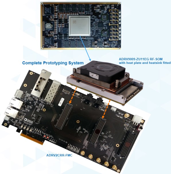
ADRV9009-ZU11EG RF-SOM Complete Prototyping System
Synchronizing multiple ADRV9009-ZU11EG RF-SOMs
The following link includes detailed description on synchronization hardware and software:
The synchronization of multiple ADRV9009 is accomplished by phase aligning the SYSREF and REFCLK fed into the transceiver and the deterministic latency of the JESD204B data path interface. The phase aligning mechanism is built around the HMC7044B, a high-performance jitter attenuator, capable of generating 14 ultralow phase noise output frequencies. Phase alignment is achieved by the pulsed SYNC or RFSYNC inputs, giving the possibility to extend the clock tree to multiple stages.
The complete prototyping system built out of ADRV9009-ZU11EG, ADRV2CRR-FMC, AD-FMCOMMS8-EBZ acts as a proof of concept for synchronizing multiple ADRV9009 transceivers. The diagram below shows the clock tree for a synchronized system consisting of eight ADRV9009 (2 carriers). With a single HMC7044B synchronization board there is the possibility of extending the number of carriers to three, totaling twelve ADRV9009 transceivers. For extending this number multiple HMC7044B synchronization boards need to be cascaded.
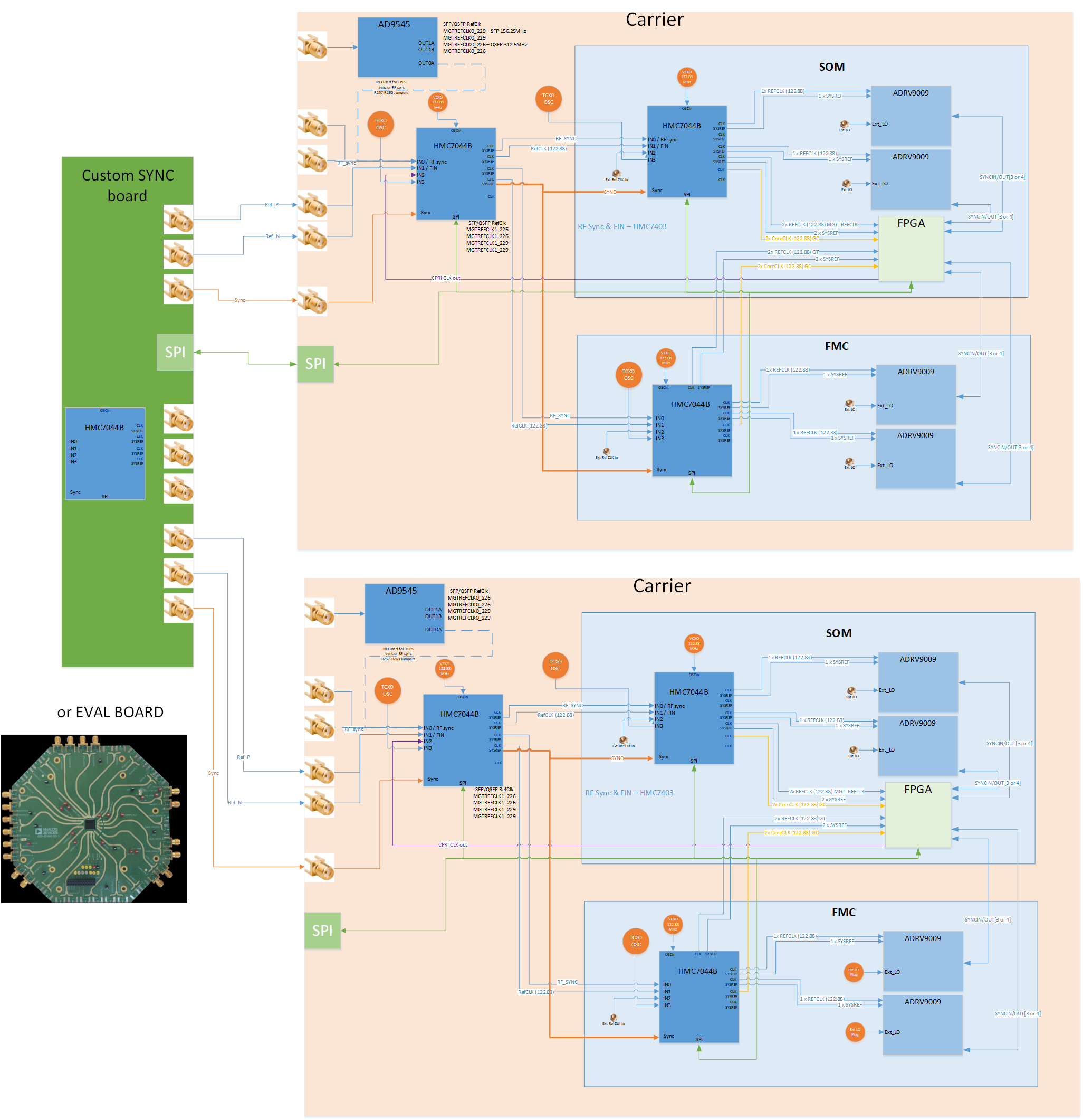
Clock Distribution
The clock generated by the first stage HMC7044B is distributed throughout the clock tree. The HMC7044B in the lower stages are acting only as fanout buffers. The synchronization is accomplished by pulses on the RFSYNC input. This architecture is easier to manage and is lower power, since only the first stage PLL and VCO are active. Since the high frequency clock signal needs to be distributed it might create routing problems.
Reference Distribution
In reference distribution the PLLs inside the HMC7044B stages are active and work as clock generators and jitter cleaners, being synchronized by the SYNC input. This architecture provides ultralow jitter and removes the risk of coupling of unwanted signals in the clock chain.
The clocking map below shows the path for both clock and reference distribution. An example is shown for VCXO of 122.88MHz and internal VCO frequency of 2919.12MHz.
Download
The System Clock Map is located here:
Thermal Considerations
Important
The ADRV9009-ZU11EG RF-SOM requires active cooling. It includes overtemperature protection, which interrupts power to the RF-SOM when board temperature reaches 90 °C. Without a fan the RF-SOM will turn off in a few minutes under normal operating conditions (25 °C ambient, Linux machine running).
The ADRV9009-ZU11EG RF-SOM comes equipped with a custom designed heat spreader plate, that acts as a mounting base for an active cooler. Panasonic EYG-T7070A10A thermal pad is used between RF-SOM and plate.
The heat spreader is designed to accommodate an active cooler with an AMD type SP3/TR4/sTRX4 socket. There are two sets of threaded holes. When thermal sheet is added between heat plate and fan the set of holes with the smaller thread depth should be used for mounting the fan.
The ADRV2CRR-FMC kit includes a heatsink with fan for the ADRV9009-ZU11EG RF-SOM, and Würth Elektronik 39410 EMI gasket sheet, that acts both as thermal transfer material between plate and heatsink, and RF Shield/Absorber.
Supplementary Testing
Download
EMC testing has been carried out on the SOM. This may be useful as a reference for validation or qualification of custom designs. The report can be found here:
Mechanical Reference Material
Download
The X-Y Footprint is located here:
The RF-SOM 3D model is located here:
The Heat spreader plate 3D model is located here:
ADRV9009-ZU11EG Schematics, BOM & Errata
Rev G is the latest hardware revision. The schematics and BOM available for download below are for earlier revisions.
Download