AD9152-EBZ Evaluation Board Quick Start Guide
Getting Started with the AD9152-EBZ Evaluation Board and Software
What’s in the Box
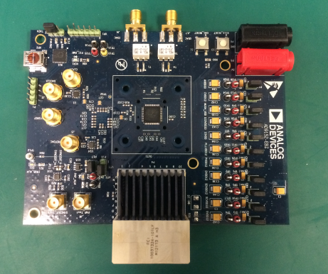
AD9152-EBZ Evaluation Board
Evaluation Board CD
Mini-USB Cable
Recommended Equipment List
+5Vdc, Power Supply
1 Sinusoidal Clock Source
Spectrum Analyzer
Data Pattern Generator Series 3 (DPG3)
Introduction
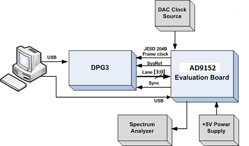
The AD9152-EBZ connects to a DPG3 for quick evaluation of the AD9152, a high-speed, signal processing Digital to Analog Converter. The DPG3 automatically formats the data and sends it to the AD9152-EBZ, simplifying evaluation of the device. The Evaluation Board (EVB) runs from a +5V supply. A clock distribution chip AD9516 is included on this EVB as a clock fan-out and frequency divider for the DACCLK, REFCLK and DPG3 input clock. Figure 2 is an image of the top side of the AD9152-EBZ.
AD9152 Evaluation Software
The AD9152 Evaluation Board software includes the ACE software application and DPGDownloader software. There is an easy-to-use legacy graphical user interface (GUI) available on the DPG website at http://www.analog.com/dpg, but ACE is the preferred evaluation method for the AD9152. ACE is included on the Evaluation Board CD or can be downloaded from the ACE website at http://www.analog.com/en/design-center/evaluation-hardware-and-software/ace-software.html. The legacy GUI and DPGDownloader software are available on the DPG website at http://www.analog.com/dpg. This will install DPGDownloader (for generating and loading vectors into the DPG3) and AD9152 SPI software.
Hardware Setup
Connect +5.0V to P5, GND to P6. A low phase noise high frequency clock source should be connected to the SMA connector, J1. This is the DACCLK input. The spectrum analyzer should be connected to the SMA connector, J4. A +1.0V power supply must be connected to the VTT probe point near SMA connector J9, along with a GND connection to the GND probe point next to it. The evaluation board connects to the DPG3 through the connectors P4. The PC should be connected to the EVB using the mini-USB connector XP2 after installation of the Evaluation Board software. Figure 1 shows the block diagram of the set-up.
Getting Started
The PC software comes on the included Evaluation Board CD, but may also be downloaded from the DPG Web site at http://www.analog.com/dpg and the ACE website at http://www.analog.com/en/design-center/evaluation-hardware-and-software/ace-software.html. The installation will include the ACE application software and the DPG Downloader software as well as all the necessary AD9152 files including schematic, board layout, datasheet, AD9152 SPI, and other files.
Initial Set-Up
Install the DPG Downloader and the ACE application software, which is preferred, or the AD9152 SPI software and support files on your PC. Follow the instructions in the installation wizard and use the default (recommended) installation settings.
Use a USB cable to connect the EVB to your PC and connect the lab equipment to the EVB.
Connect the DGP3 unit to your PC and turn on the unit.
Single-Tone Test
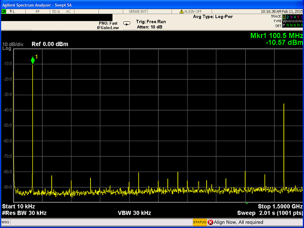
These settings configure the AD9152 to output a sine wave using the DPG3 and allow the user to view the single-tone performance at the DAC output, under the condition: Fdata = 375MHz, 4X interpolation, Fout = 100MHz.
Using ACE
Configure DPG Vector Software
To begin, turn on the external +5V supply.
Open DPG Downloader if you have not done so. (Start > All Programs > Analog Devices > DPG > DPGDownloader). Ensure that the program detects the AD9152, as indicated in the “Evaluation Board” drop-down list, and select it.
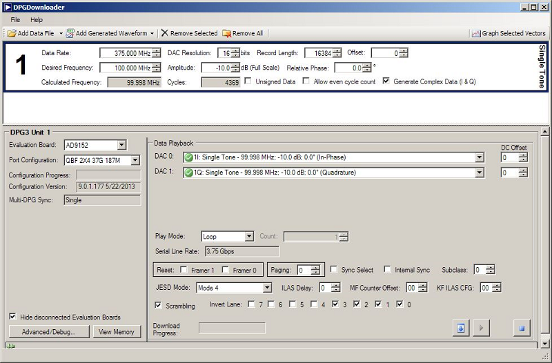
Set “Port configuration” to “2X4 37G 187M ” in the DPG Downloader panel and select Mode 4 in the JESD Mode drop-down box.
Click on “Add Generated Waveform”, and then “Single Tone”. A Single Tone panel will be added to the vector list. Enter the Data Rate, in this case 375MHz and the desired frequency, 100MHz. Enter the digital amplitude. In this case we use -10dBFS. Uncheck the “Unsigned Data” box, check the “Generate complex data (I & Q)”, as in Figure 3.
Select the data vector of 100MHz desired frequency ’in-phase’ data in the “DAC0” drop down menu and the ‘Quadrature’ data in the “DAC1”. At this point, the DPG Downloader panel should look like Figure 3.
Configure the ACE Software
Open ACE from the start window. It can be found by following the file path to the program or by searching in the windows search bar for “ACE.” The
 icon indicates the ACE software.
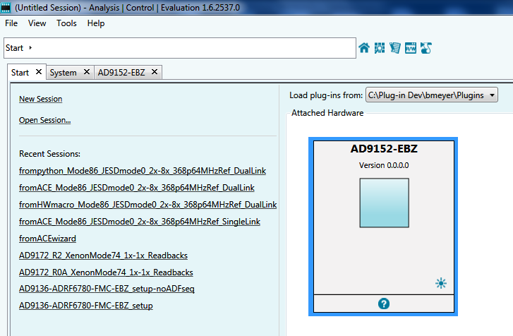
If the board is connected properly, ACE will detect it and display it on the Start page under “Attached Hardware.” Double click this board.
Ensure that the
 button is green in the subsystem image under the “System” tab. If not, click it, select the AD9152, and click “Acquire.” Double click on the subsystem image.
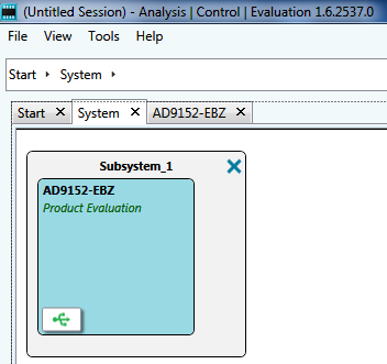
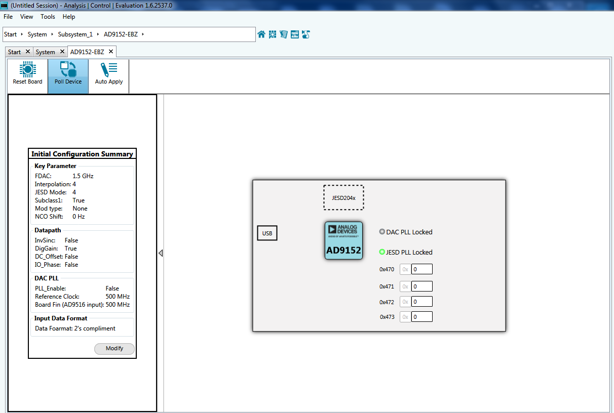
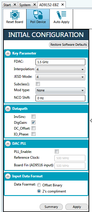
Figure 6 Inputs for the Initial Configuration of the AD9152.
At this point the data clock frequency on the LED panel of the DPG3 should read 187MHz and the Serial Line Rate in the DPG3 software panel should read 3.75Gbps. Click Download (
 ) and Play (
 ) in the DPG Downloader screen.
The current on the 5V supply should read about 1256mA. If you do not see the output, gently push the board toward the DPG3. This ensures that the board is firmly connected to the DPG3. The four registers codeGrpSync, FrameSync, GoodCheckSum and Initial LaneSync should all read 0F indicating the lanes are working correctly.
Using the Legacy SPI Application
Configure DPG Vector Software
To begin, turn on the external +5V supply.
Open DPG Downloader if you have not done so. (Start > All Programs > Analog Devices > DPG > DPGDownloader). Ensure that the program detects the AD9152, as indicated in the “Evaluation Board” drop-down list, and select it.
Set “Port configuration” to “2X4 37G 187M ” in the DPG Downloader panel and select Mode 4 in the JESD Mode drop-down box.
Click on “Add Generated Waveform”, and then “Single Tone”. A Single Tone panel will be added to the vector list. Enter the Data Rate, in this case 375MHz and the desired frequency, 100MHz. Enter the digital amplitude. In this case we use -10dBFS. Uncheck the “Unsigned Data” box, check the “Generate complex data (I & Q)”, as in Figure 3.
Select the data vector of 100MHz desired frequency ’in-phase’ data in the “DAC0” drop down menu and the ‘Quadrature’ data in the “DAC1”. At this point, the DPG Downloader panel should look like Figure 3.
Configuring SPI
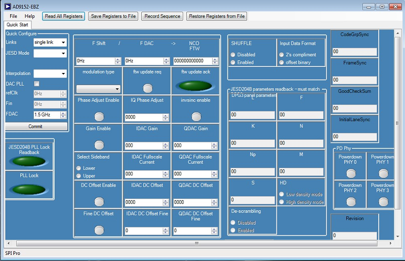
Open the AD9152 SPI application (Start > All Programs > Analog Devices > AD9152 > AD9152 SPI). The screen should look similar to Figure 11.
Configure the hardware according to the hardware set-up instructions given in the Hardware Setup section above. Set the frequency of the DAC clock signal generator to 1.5GHz, and the output level to +3dBm. The spectrum analyzer can be configured with Start Frequency = 10 MHz, Stop Frequency = 1.5GHz, and Resolution Bandwidth of 30 kHz. Choose Input Attenuation to be 10dB. This can be adjusted later if indications are that the analyzer is causing degradations.
Follow the sequence below to configure the AD9152 SPI registers.
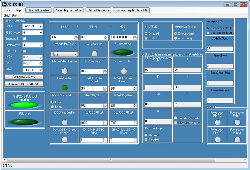
The Links should be set to single link. The JESD Mode is set to 4, Interpolation set to 4, and FDAC set to 1.5GHz. Click “Commit” button to initialize the AD9152. The JESD204B PLL should be locked indicated with bright green JESD204B PLL readback LED.
At this point the data clock frequency on the LED panel of the DPG3 should read 187MHz and the Serial Line Rate in the DPG3 software panel should read 3.75Gbps.
Click “Read All Registers” in the top menu bar. You should see “JESD204B PLL Lock Readback” LED readback is bright green indicating that the SERDES PLL is locked.
Click Download (
) and Play () in the DPG Downloader screen.The current on the 5V supply should read about 1256mA. If you do not see the output, gently push the board toward the DPG3. This ensures that the board is firmly connected to the DPG3. The four registers codeGrpSync, FrameSync, GoodCheckSum and Initial LaneSync should all read 0F indicating the lanes are working correctly.
ACE Software Features
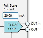
The ACE software is organized to allow the user to evaluate and control the AD9122A evaluation board. The “Initial Configuration” wizard, which is only available for certain boards, controls the DAC and PLL setups. Block diagram views of the board and chip contain elements that can be used to vary parameters like ref current and data format. These parameters can be changed using check boxes, drop down menus, and input boxes. Some parameters do not have settings shown in the diagram. Double click on the parameter to view the available settings, seen with the NCO settings below.
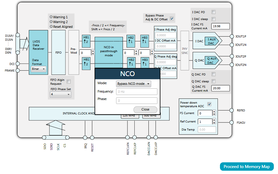
NCO settings for the AD9122
In addition, some parameters can be enabled or disabled. This feature is evident by the color of the block parameter. For example, if the block parameter is dark blue, the parameter is enabled. If it is light grey, it is disabled. To enable or disable a parameter, click on it.
Enabled parameter
Disabled parameter
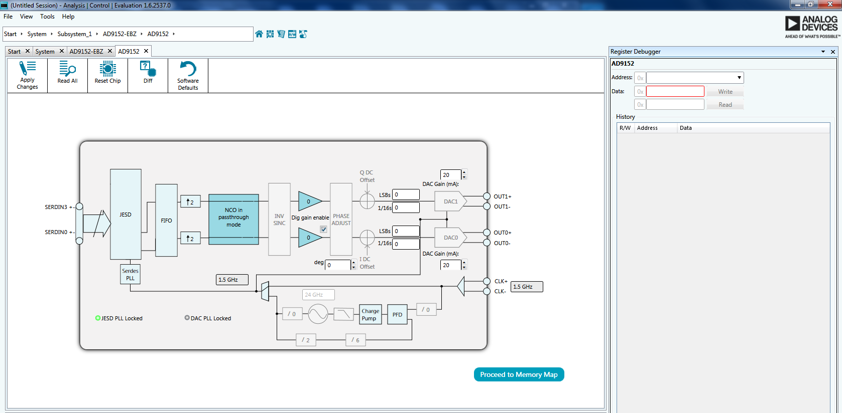
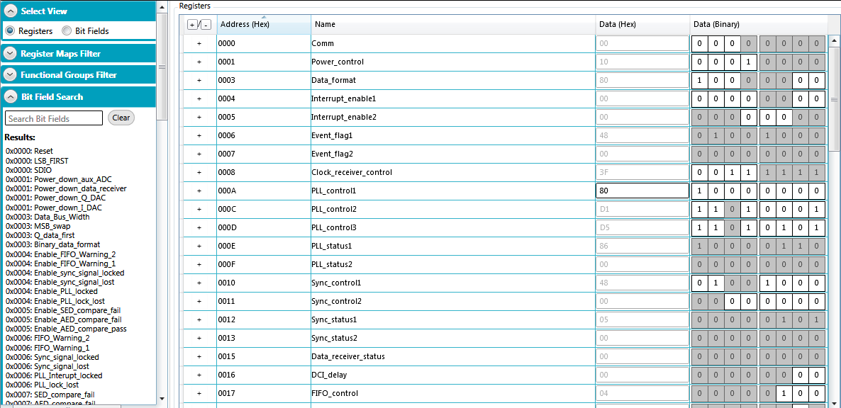
More direct changes to registers and bit fields can be made in the memory map, which is linked from the chip block diagram through the “Proceed to Memory Map” button. In this view, names, addresses, and data can be manually altered by the user.
Bench Set-Up
ACE also contains the Macro Tool, which can be used to record register reads and writes. This is executed in the memory map view or with the initialization wizard. To use, check the “Record Sub-Commands” checkbox and press the record button. Changes in the memory map, which are bolded until they are applied to the part, are recorded as UI commands by the macro tool once the changes are made. Changed register write commands for the controls are also recorded. Hit “Apply Changes” to execute the commands and make changes in the memory map. To stop recording, click the “Stop Recording” button. A macro tool page with the command steps will be created. The macro can be saved using the “Save Macro” button so that it may be loaded for future use.
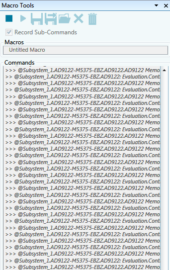
Macro tool in ACE. The Stop Recording, Record, and Save Macro commands are located at the top of the macro tool.
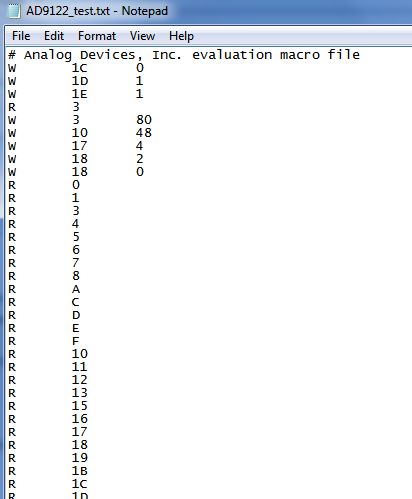
The raw macro file will be saved using ACE syntax, which is not easily readable. To remedy this, the ACE software download includes the Macro to Hex Conversion Tool. The user can choose to include or exclude register write, reads, and/or comments in the conversion. The file pathways for the source and save paths should be the same, except that one should be an .acemacro file and the other should be a .txt file. The “Convert” button converts and opens the converted text file, which is easier to read. The conversion tool can also convert back to an .acemacro file if desired.
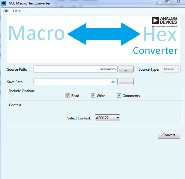
Conversion set-up for macro to hex
Converted text file
For more information about ACE and its features, visit https://wiki.analog.com/resources/tools-software/ace.
Note
In single link JESD204B mode 4,5,6,7,9,10, the Serdes line cross-bar setting as shown below, are added in this software to match the data mapping the DPG3 requires. They are not required if the data source is not a DPG3. write(0x308,0x08) write(0x309,0x1A)