

ADMX6020M HDL Project
Overview
The ADMX6020M is a dual-channel HMCAD15xx ADC data acquisition system targeting Xilinx Zynq-7000. It supports synchronous capture from both ADCs in all supported resolutions (8/12/14-bit) for up to 64KB of data per channel.
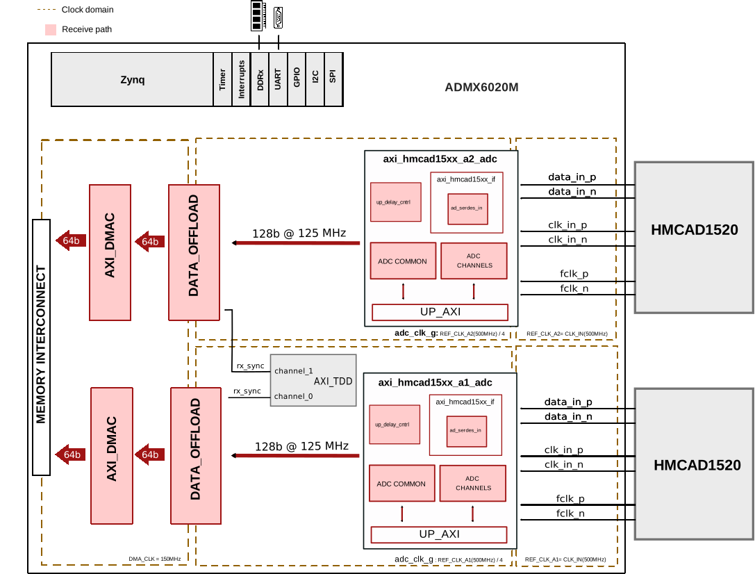
The design uses the TDD IP to generate a sync signal that triggers simultaneous capture start on both ADC channels, ensuring sample-aligned data acquisition.
Key features:
1 GSPS sampling rate (1 ns time resolution) / 8-bit vertical resolution
2 differential input channels
50-ohm input impedance
0°C to 85°C(ambient)
Configurable input range (0.5V to 1.5V default, configurable to -4V min to +4V max)
Built-in non-volatile storage
Programmable trigger functionality
SPI, I2C, USB interfaces for control and data offloading
Supported boards
ADMX6020M
Supported devices
Block design
The design implements a dual ADC capture system with BRAM-based data offload for synchronized acquisition. Each ADC channel has its own data path consisting of an LVDS interface, BRAM buffer, and DMA engine.
Block diagram
The data path and clock domains are depicted in the below diagram:
Clock scheme
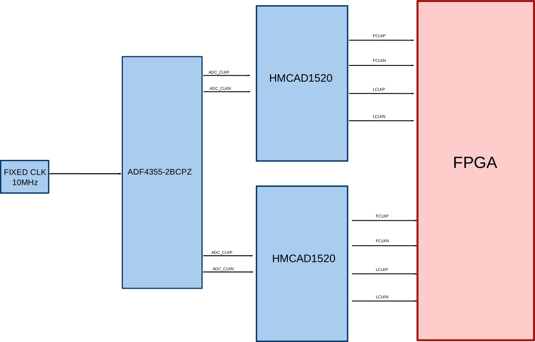
The design uses the following clock domains(all the rates are described at the highest sampling rate of 1 GSPS):
Clock |
Frequency |
Description |
|---|---|---|
FCLK_CLK0 |
100 MHz |
CPU clock, AXI register access |
FCLK_CLK1 |
200 MHz |
IODELAY reference clock |
FCLK_CLK2 |
150 MHz |
DMA clock DATA offload output |
ref_clk_a1/a2 |
500 MHz |
ADC LVDS input clock (from ADF4355) |
adc_clk/adc_clk_1 |
125 MHz |
Divided ADC clock (ref_clk/4) |
The ADF4355 PLL provides the 1GHz reference clock to both ADCs which then is sent to the FPGA as the 500MHz reference clock(ref_clk_a1/a2). The LVDS interface deserializes the DDR data and divides the clock by 4 to produce the 125 MHz sample clock.
Configuration modes
The design supports the following ADC operating modes controlled via SPI:
8-bit mode: 1 GSPS, single channel
12-bit mode: 500 MSPS, single channel (HMCAD1511)
dual 8-bit mode (14-bit resolution): 125 MSPS, 4 channels interleaved (HMCAD1520)
The axi_hmcad15xx IP parameters:
Parameter |
Description |
|---|---|
NUM_CHANNELS |
Number of ADC channels (1-4) |
IODELAY_CTRL |
Set to 1 for one instance only (shared IDELAYCTRL) |
CPU/Memory interconnects addresses
The addresses are dependent on the architecture of the FPGA, having an offset added to the base address from HDL (see more at CPU/Memory interconnects addresses).
Instance |
Zynq |
|---|---|
axi_iic_main |
0x4160_0000 |
axi_hmcad15xx_a1_adc |
0x44A0_0000 |
hmcad15xx_a1_dma |
0x44A3_0000 |
axi_hmcad15xx_a2_adc |
0x44A6_0000 |
hmcad15xx_a2_dma |
0x44A9_0000 |
axi_tdd_sync |
0x44AC_0000 |
adc1_data_offload |
0x44B0_0000 |
adc2_data_offload |
0x44B1_0000 |
I2C connections
I2C type |
I2C manager instance |
Alias |
Address |
I2C subordinate |
|---|---|---|---|---|
PL |
axi_iic_main |
— |
0x34 |
ADP5589 (GPIO expander) |
PL |
axi_iic_main |
— |
0x0C |
AD5696 (DAC) |
PL |
axi_iic_main |
— |
0x5F |
MAX31827 (temperature sensor) |
SPI connections
SPI type |
SPI manager instance |
SPI subordinate |
CS |
|---|---|---|---|
PS |
SPI 0 |
HMCAD15xx (ADC1) |
0 |
PS |
SPI 0 |
HMCAD15xx (ADC2) |
1 |
PS |
SPI 0 |
ADF4355 (PLL) |
2 |
GPIOs
GPIO signal |
Direction |
HDL GPIO EMIO |
Software GPIO |
|---|---|---|---|
(from FPGA view) |
Zynq-7000 |
||
ad9696_ldac |
INOUT |
0 |
54 |
Interrupts
Below are the Programmable Logic interrupts used in this project.
Instance name |
HDL |
Linux Zynq |
Actual Zynq |
|---|---|---|---|
axi_iic_main |
15 |
59 |
91 |
hmcad15xx_a2_dma |
13 |
57 |
89 |
hmcad15xx_a1_dma |
12 |
56 |
88 |
Building the HDL project
The design is built upon ADI’s generic HDL reference design framework. ADI distributes the bit/elf files of these projects as part of the ADI Kuiper Linux. If you want to build the sources, ADI makes them available on the HDL repository. To get the source you must clone the HDL repository.
Go to the hdl/projects/admx6020m location and run the make command.
Linux/Cygwin/WSL
~$
cd hdl/projects/admx6020m
~/hdl/projects/admx6020m$
make
A more comprehensive build guide can be found in the Build an HDL project user guide.
Resources
More information
Support
Analog Devices, Inc. will provide limited online support for anyone using the reference design with ADI components via the EngineerZone FPGA reference designs forum.
For questions regarding the ADI Linux device drivers, device trees, etc. from our Linux GitHub repository, the team will offer support on the EngineerZone Linux software drivers forum.
For questions concerning the ADI No-OS drivers, from our No-OS GitHub repository, the team will offer support on the EngineerZone microcontroller No-OS drivers forum.
It should be noted, that the older the tools’ versions and release branches are, the lower the chances to receive support from ADI engineers.