User guide
The complete user guide of the evaluation board can be found at ADRV9001/ADRV9002 System Development User Guide (UG-1828).
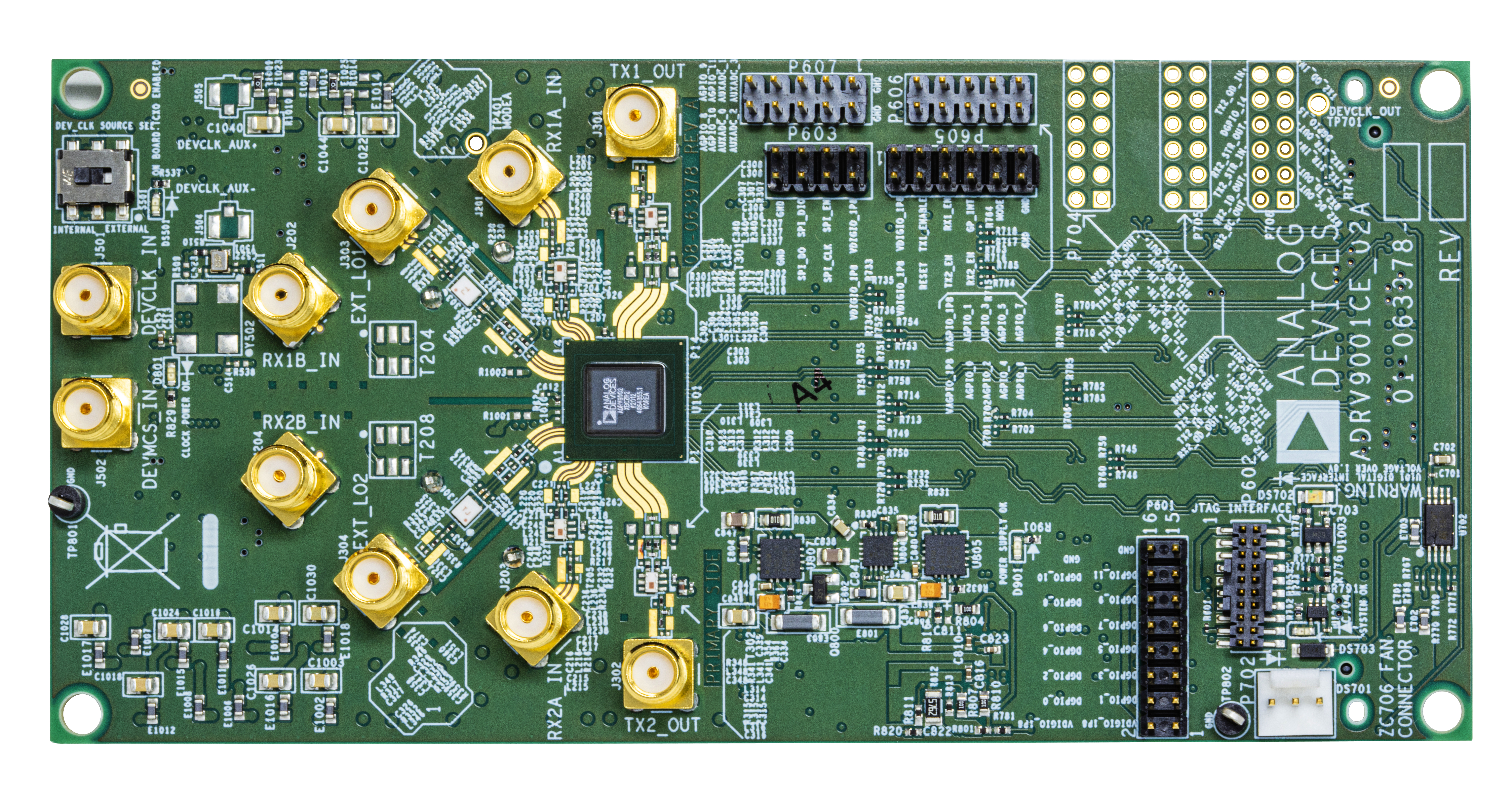
Hardware guide
Power supply
The power supply comes from the FMC connector, given by the FPGA carrier board.
The ADRV9002 evaluation board uses the ADP5056 power management IC to generate the required internal power domains. The board requires 1.8V on the VADJ supply for the transmitter/receiver DACs/ADCs and GPIO signals.
The VADJ configuration for each FPGA carrier board can be found in the README.md file at: projects/adrv9002.
Clock configuration
The ADRV9002 evaluation board supports multiple clock configuration options:
Clock source selection
On the FMC card, set the “DEV_CLK Source Sel.” switch to select clock source between:
Internal (default): On-board 38.4 MHz VCTCXO
Low phase noise crystal oscillator
Suitable for most applications
No external clock generator required
External: Via J501 connector
Frequency range: 10 MHz to 1000 MHz
Input power level: +13 dBm
Allows use of high-quality external reference clock for optimal performance
Note
The quality of the clock source used to generate the DEV_CLK directly impacts the overall system performance. Use a high-quality, stable, and low-phase noise clock source.
Internal synthesizers
The ADRV9002 employs four PLL synthesizers for flexible clock generation:
Clock PLL: Generates digital clocks for ADC/DAC and LVDS interface
RF PLL 1: Generates LO1 for transmitter/receiver channel 1
RF PLL 2: Generates LO2 for transmitter/receiver channel 2
Auxiliary PLL: Generates auxiliary LO for calibration
Each PLL features:
Fractional-N architecture for flexible frequency synthesis
Integrated VCO with tuning range of 6.5 GHz to 13 GHz
RF LO frequency range: 30 MHz to 6000 MHz
Programmable loop filter bandwidth for phase noise optimization
External LO mode
The ADRV9002 supports external LO input for advanced applications:
Differential external LO: 60 MHz to 12 GHz with 100 Ω differential impedance
Single-ended external LO: 500 MHz to 1 GHz with 50 Ω impedance
Programmable signal level: ±6 dBm typical
Can be configured independently for each RF channel
RF and data interfaces
The evaluation board provides:
RF ports: SMA connectors for:
Dual receiver channels: RX1A±, RX1B±, RX2A±, RX2B±
Dual transmitter channels: TX1±, TX2±
Frequency range: 30 MHz to 6000 MHz covering VHF, UHF, ISM, and cellular bands
Bandwidth: 12 kHz to 40 MHz (configurable via profile)
Data interface: CMOS or LVDS synchronous-serial interface to FPGA
Control interface: 4-wire SPI for device configuration
Data interface modes
The ADRV9002 supports both CMOS and LVDS synchronous serial interfaces.
The mode is selected at HDL build time (CMOS_LVDS_N parameter),
producing separate boot files for each mode.
On carriers that support both interfaces (e.g., ZCU102), two BOOT.bin files are provided — select the one matching your desired mode.
However, not all carriers support LVDS. Refer to the supported carriers table for details on per-carrier interface availability.
See also
AXI ADRV9001 HDL Library for full details on supported configurations per mode.
Device modes
The ADRV9002 HDL design supports two device modes, each requiring a different devicetree:
Independent mode (
adi,adrv9002): Both channels are treated separately by the HDL core, each with its own DMA buffer. Suitable for TDD implementations.MIMO mode (
adi,adrv9002-rx2tx2): A single DMA buffer is used and both RX1/RX2 physical ports are mapped into the RX1 channel in the HDL AXI core. Suitable for diversity applications requiring identical baseband sample rates across channels.
When setting up the SD card, select the devicetree file that matches your desired mode.
See also
ADRV9002 for more details on device modes and devicetree configuration.
Analog inputs
Connect RF signals to the SMA connectors on the evaluation board:
Use appropriate RF signal generators or antennas for the receiver inputs
Ensure signal levels are within the specified input range
For transmitter testing, connect to spectrum analyzers or RF power meters
Maintain proper impedance matching (typically 50 Ω) for optimal performance
Schematic, PCB Layout, Bill of Materials
Design files for the ADRV9002 evaluation board including schematics, PCB layout, bill of materials, and reference designs are available at:
Software guide
The ADRV9002 evaluation board is supported with the libiio library. This library is cross-platform (Windows, Linux, Mac) with language bindings for C, C#, Python, MATLAB, and others.
ADI IIO Oscilloscope
The IIO Oscilloscope is a cross-platform application for interfacing with IIO devices, enabling you to configure device parameters and visualize data.
Important
Make sure to download/update to the latest version of IIO Oscilloscope.
For Linux
Remote run on host
The IIO Oscilloscope application can be used to connect to another platform that has a connected device, to configure the device and read data from it. This application is not for performance testing, but rather showcasing the basic features.
Please see IIO Oscilloscope documentation for installation steps and more details.
Build and start osc on a network-enabled Linux host.
For Windows computers, open the application from the start menu.
Once the application is launched, go to Settings > Connect > URI and type “ip:” then the IP address of the target in the pop-up window. This IP can be found out with a command from the previous section of this documentation.
For no-OS
For connecting IIO Oscilloscope to no-OS applications, they need to be built with the IIOD=y flag. This way, the no-OS applications will run an IIO daemon that is awaiting connections from the IIO Oscilloscope.
As indicated in the boot log, the board runs an IIOD server over the serial (UART) connection.
Disconnect or close the serial terminal used to view the boot log.
Once done with the installation or an update of the latest IIO Oscilloscope, open the application.
Select the Serial backend and configure the connection with the settings shown at the end of the boot log.
Press Refresh to display the available IIO devices and press Connect.
Note
The serial port is the COM port on Windows or /dev/ttyUSBx on Linux.
Plugin
This project also contains an IIO-Oscilloscope device-specific plugin that enables you to access the unique features and functions of the device.
See also
For more information about this plugin: ADRV9002 Plugin Description
Data capture
Note
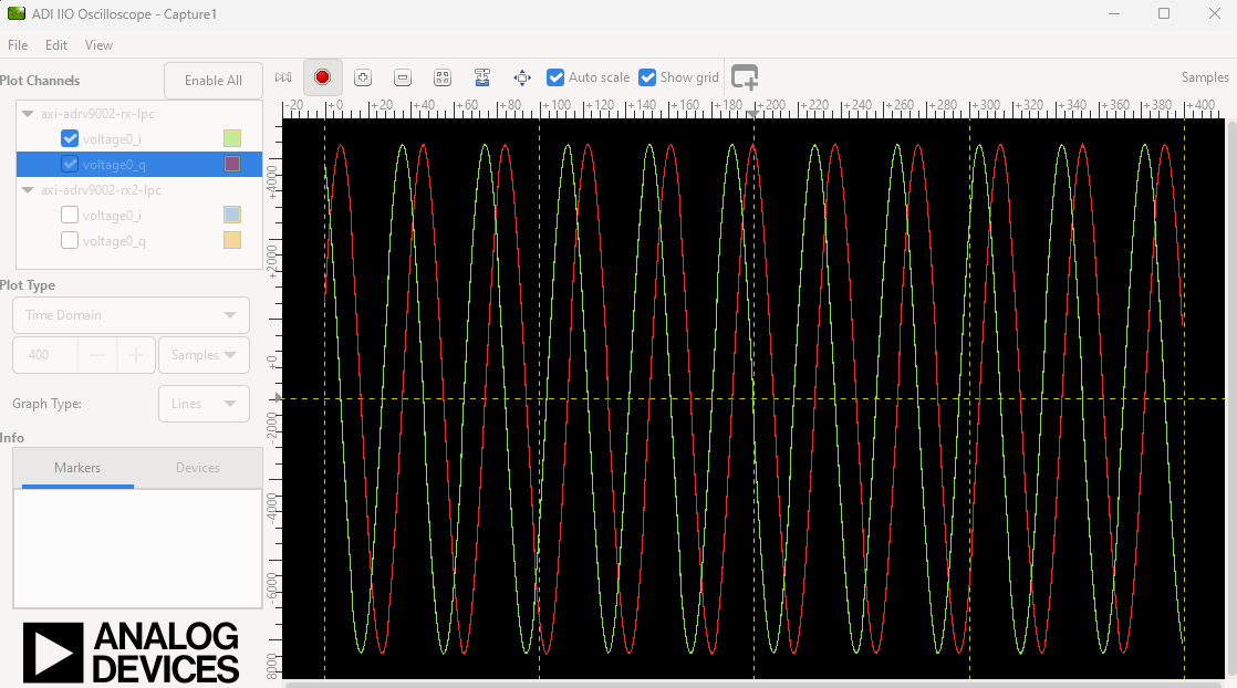
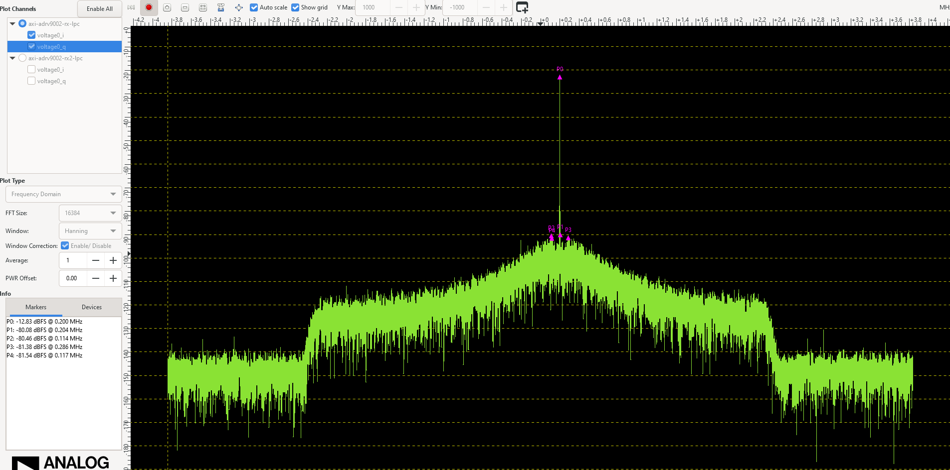
Device names and channel definition may differ between no-OS and Linux.
Time domain:
Frequency domain:
Scopy
Scopy is a cross-platform software toolbox for interfacing with ADI devices, enabling you to configure device parameters, visualize data, and perform advanced signal analysis.
Plugin
This project also contains a Scopy device-specific plugin that enables you to access the unique features and functions of the device.
See also
Find more information about this plugin here
PyADI-IIO
PyADI-IIO is a Python abstraction module for ADI hardware with IIO drivers. An ADRV9002 example can be found here.
MATLAB
ADRV9002 support through Transceiver Toolbox
GNU Radio
ADRV9002 integration with GNU Radio
Linux Driver
The ADRV9002 Linux kernel driver provides device initialization, profile configuration, dynamic profile switching, tracking calibrations, ENSM control, GPIO/AuxDAC/AuxADC access, and power management.
See also
No-OS
ADRV9002 bare-metal driver for embedded applications.
See also
HDL Testbench
The ADRV9001 provides a simulation environment for verifying the HDL reference design using SystemVerilog and the Xilinx toolchain. The testbench source can be found here.