SDP-H1 Quickstart
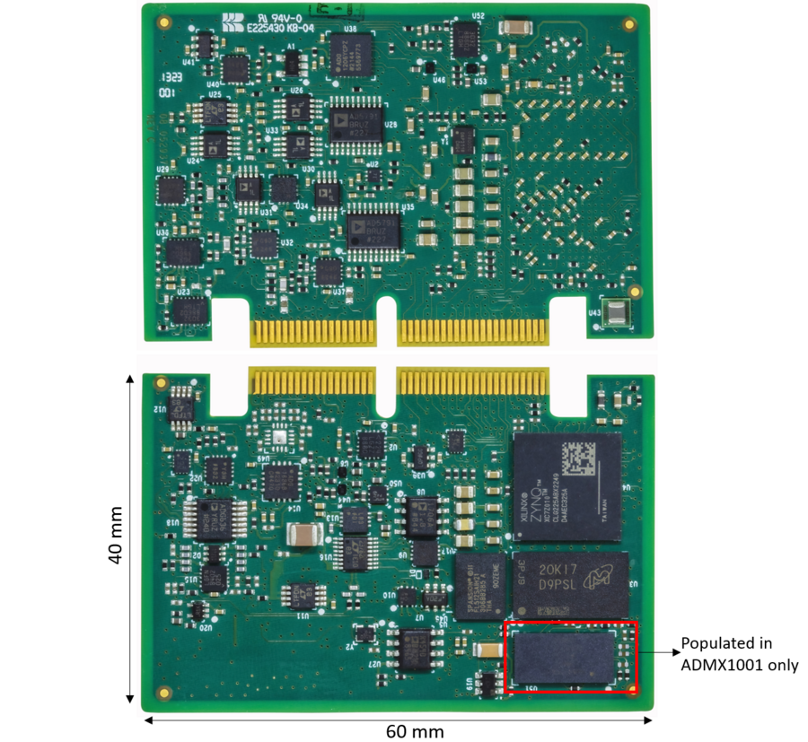
The ADMX1001 and ADMX1002 modules are ultra-low distortion and low-noise signal generators. They have a frequency range of up to 40 kHz when not using the digital pre-distortion (DPD) algorithm. If the DPD algorithm is enabled for signal generation, they can generate tones up to 20 kHz with -130dB typical of total harmonic distortion (THD) at 1 kHz. In addition to signal generation, the ADMX1001 includes a differential input acquisition channel to measure a signal of choice.
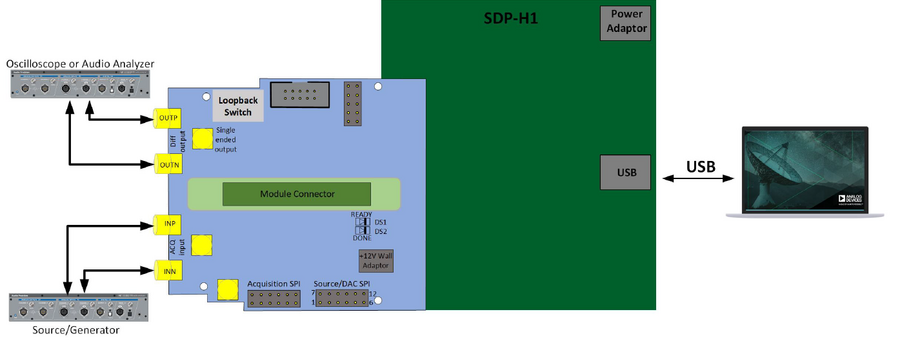
These modules can be evaluated with a single GUI to generate different signals. The PC GUI connects to an SDP controller board via USB that has established SPI communication to the module. The recommended controller board is the SDP-H1 which connects to the EVAL-ADMX100X-FMCZ’s FMC connector.
Additional Equipment Needed
Controller Board Option 1 (Use with ADMX1002 only)
-
USB-A to mini-USB cable
SDP-I-PMOD interposer board
6V Power Adapter
6-Pin PMOD Cable
-
Controller Board Option 2 (Use with ADMX1001 or ADMX1002)
SDP-H1 controller board
USB-A to mini-USB cable
12V Power Adapter
SMA cables for output connection
Oscilloscope/Audio analyzer
Software Needed
Installing SDP USB Drivers
Download
SDPDrivers.exefrom the SDP Drivers Installation Instructions.Run the installer and follow the on-screen instructions.
Accept the license agreement, select the installation location, and click Install.
Reboot the PC if prompted.
Installing the ADMX100X GUI
To install the ADMX100X GUI, take the following steps:
Download the executable available in the Software section of the product page or click on the link: ADMX100x GUI Download
Double-click on the Admx100xEvaluationSoftware-Relx.x.x_EVAL.exe file from the downloads folder to begin the installation.
Note
The installer may require the user to have administrator privileges for the machine
The installer will begin to load, with the progress window visible on the desktop.
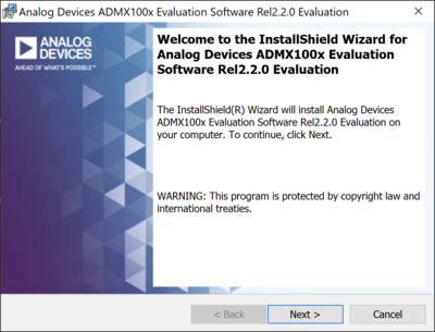
Once the Installer has loaded, the welcome screen will appear. Click Next.
Accept the license agreement on the following screen with the radio button and click Next.
The default installation location is C:\Analog Devices\. If another location is desired, click the Change… button on the following screen and navigate to the desired location. Click Next > once the installation location is finalized.
The installation can now begin. Click Install to proceed.
Once the installation has finished, a window will appear confirming it is completed and give an option to view the Release Notes (opted-in by default). Click Finish to close the installer.
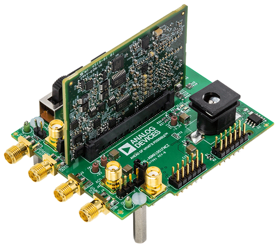
Hardware Setup
ADMX100X Module connector: The ADMX1001 or ADMX1002 module is connected to the EVAL-ADMX100X-FMCZ evaluation board via (P5) module connector.
FMC connector: The SDP-H1 will connect to the FMC connector that is on the bottom of the board.
Power Supply: The EVAL-ADMX100X-FMCZ evaluation board is powered from a 12V wall adaptor via P14. The evaluation board provides on-board supply regulators to generate the +3.3V and ±9V required to power the module.
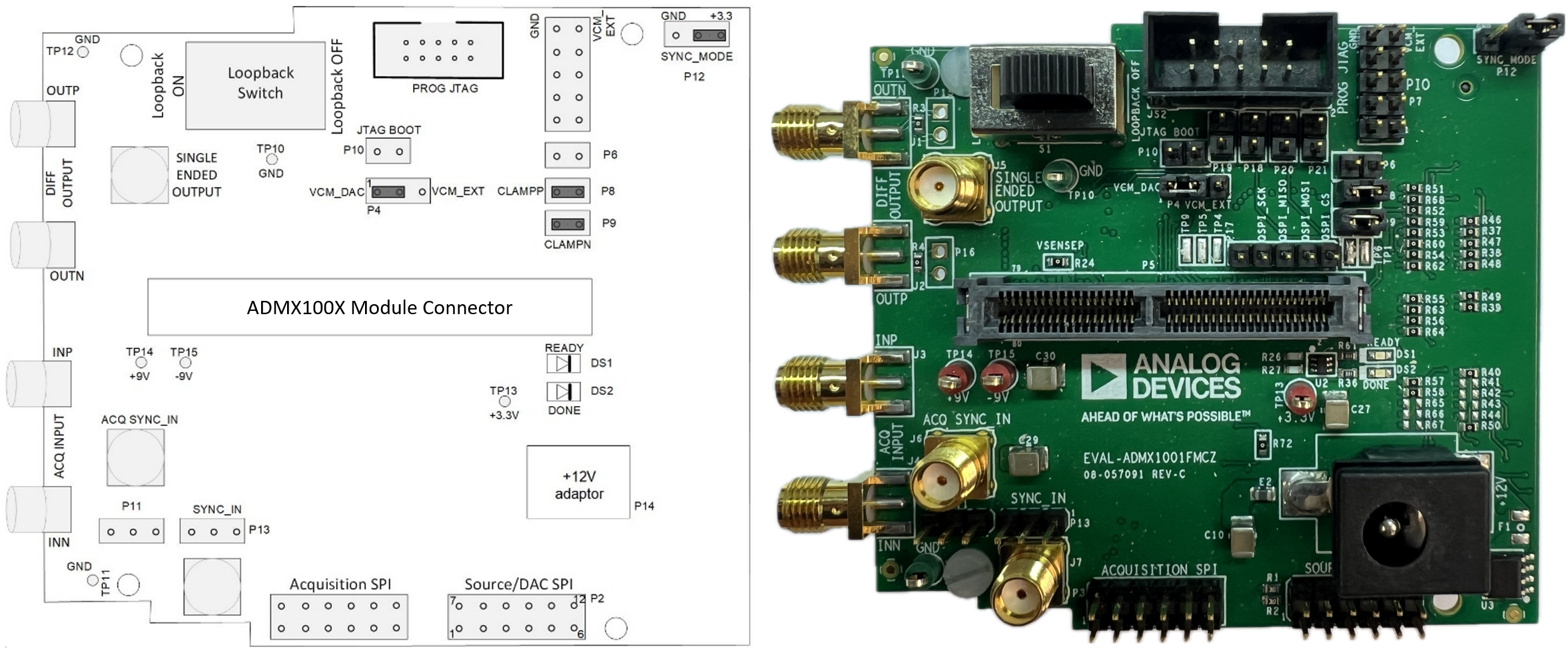
SMA connector descriptions are summarized in Table 1.
Jumpers and Switch Setup are summarized in Table 2.
Name |
Function |
Position |
|---|---|---|
P4 [1] |
VCM from DAC or external |
2-1 (VCM_DAC) |
P6 |
EN |
Removed |
P8 |
Sense input clamp to +5 V |
Inserted |
P9 |
Sense input clamp to −5 V |
Inserted |
P10 |
JTAG_BOOT |
Removed |
P11 |
ACQ_SYNC_IN |
Removed |
P12 |
SYNC_MODE |
2-1 (+3.3 V) |
P13 |
SYNC_IN |
Removed |
S1 [2] |
Signal loopback enable |
Loopback Off |
The following pieces of equipment are required to perform a full evaluation:
ADMX1001 or ADMX1002 module
EVAL-ADMX100X-FMCZ kit that contains:
EVAL-ADMX100X-FMCZ evaluation board
Power adaptor
SDP controller board
SDP-H1 controller board
ADMX100X GUI software that will run on Windows 10
SMA cables for connection from EVAL-ADMX100X-FMCZ evaluation board to analyzer or oscilloscope
Follow the steps below to set up the full evaluation board.
Check that the Jumper & Switch settings match the desired configuration in Table 2.
Connect the ADMX1001 or ADMX1002 module to the module connector (P5) on the EVAL-ADMX100X-FMCZ evaluation board.
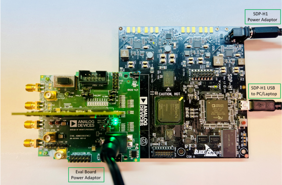
Connect the SDP-H1 controller board to the EVAL-ADMX100X-FMCZ evaluation board’s FMC connector (P1).
Connect the SDP controller USB to the computer.
Apply the SDP-H1 board power.
Apply the EVAL-ADMX100X-FMCZ power.
After the power is applied, the “READY” LED turns on and then turns off. Then the “DONE” LED turns on and the “READY” LED turns on again.
Caution: If both LEDs do not turn on, power cycle the EVAL-ADMX100X-FMCZ evaluation board.
Configure the LOOPBACK switch (S1).
If using the ADMX1002 or there is a need to view the source outputs via the OUTP and OUTN SMAs when using the ADMX1001, slide S1 on the EVAL-ADMX100X-FMCZ to the “LOOPBACK OFF” position.
If using the ADMX1001, the signal generator outputs can be looped back into the acquisition channel inputs by sliding S1 on the EVAL-ADMX100X-FMCZ to the “LOOPBACK ON” position The SMA outputs (OUTP and OUTN) and inputs (INP and INN) connectors are disengaged in this mode.
Start the ADMX100X GUI.
The GUI will display “Connected” in green text at the bottom left corner if the connection was successful.
Caution: If the GUI does not connect at this step, disconnect the GUI and power off and on the EVAL-ADMX100X-FMCZ evaluation board by removing and then reinserting the power adapter. Then start the GUI again.
Using the SDP-S or SDP-B with the SDP-I-PMOD Controller Boards
The recommended controller board to use with the EVAL-ADMX100X evaluation system is the SDP-H1. However, it is possible to use the SDP-S or SDP-B with the SDP-I-PMOD interposer board to connect to the ADMX1002B module.
Important
The SDP-I-PMOD is used in conjunction with either the SDP-S or the SDP-B boards to establish SPI communication to the ADMX1002 using only the SPI PMOD connector. The SDP-H1 performs the same function and can be plugged into the FMC connector on the EVAL-ADMX100X-FMCZ.
There are additional connections to the FMC connector that are required for some features, including the ability to shift the VCM of the generated output using the GUI, as well as access an additional SPI bus to control the acquisition module on the ADMX1001. Therefore, we recommend using the SDP-H1 controller board in most cases to access all features and both module boards (ADMX1001B and ADMX1002B). However, if the user is evaluating the ADMX1002 and can shift the VCM of the output manually, the SDP-S/SDP-B and SDP-I-PMOD boards can be used. This setup cannot be used to evaluate the ADMX1001B.
Quick Start with the SDP-S/SDP-B and SDP-I-PMOD
Refer to the EVAL-ADMX100X-FMCZ Connector layout.
Source/DAC SPI PMOD header: The SDP-S or SDP-B will communicate to the module via SPI through the Source/DAC SPI PMOD header (P2). The P2 bottom row pins 1-6 are “SS_MOSI_MISO_SCLK_GND_+3.3V”
When using these controller boards, the output common-mode voltage can only be adjusted by providing external VCM at pin 9 of P7. The P4 jumper should also be inserted at 2-3 position as indicated in Table 2.
Equipment
Figure below illustrates the required setup to evaluate the ADMX1002 module. The following pieces of equipment are required for this controller board setup:
ADMX1001 or ADMX1002 module
EVAL-ADMX100X-FMCZ kit that contains:
EVAL-ADMX100X-FMCZ evaluation board
Power adaptor
SDP controller board
SDP-S or SDP-B controller board
USB-A to mini USB cable
SDP-I-PMOD interposer board
6V Power Adapter
6-Pin PMOD Cable
ADMX100X GUI software that will run on Windows 10
SMA cables for connection from EVAL-ADMX100X-FMCZ evaluation board to analyzer or oscilloscope
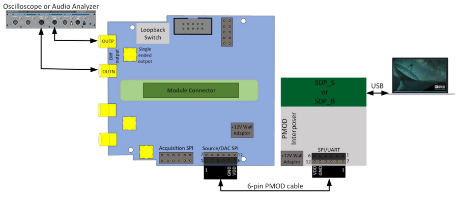
Figure 7 Evaluation Board Connection Using the SDP-I-PMOD with Either the SDP-S or SDP-B Controller Boards
Setup
Follow the steps below to set up the full evaluation board.
Check that the Jumper & Switch settings match the desired configuration in Table 2.
Connect the ADMX1002 module to the module connector (P5) on the EVAL-ADMX100X-FMCZ evaluation board.
Connect the SDP-S or SDP-B controller boards to the SDP-I-PMOD interposer board.
Put jumper JP1 into the SPI position
Caution: Remove jumper JP2
Connect the SDP-I-PMOD interposer board to the “SOURCE/DAC SPI” header (P2) on the EVAL-ADMX100X-FMCZ evaluation board through the 6-pin PMOD cable.
Connect the 6-pin male-to-male header to one end of the 6-pin PMOD cable.
Caution: Connect the male pins to the top row (pin 1-6) of the SDP-I-PMOD PMOD connector (P4). Be careful to match pin number 1 of the PMOD cable with pin number 1 of the PMOD connector (P4) on the SDP-I-PMOD board.
Caution: Connect the female side of the PMOD cable to the bottom row of the “SOURCE/DAC SPI” header (P2) on the EVAL-ADMX100X-FMCZ. Be careful to connect pin number 1 of the PMOD cable to pin number 1 of the “SOURCE/DAC SPI” header (P2).
Connect the SDP controller USB to the computer.
Apply the SDP-I-PMOD board power. Wait 10 seconds after applying power before moving to the next step.
Apply the EVAL-ADMX100X-FMCZ power.
After the power is applied, the “READY” LED turns on and then turns off. Then the “DONE” LED turns on and the “READY” LED turns on again.
Caution: If both LEDs do not turn on, power cycle the EVAL-ADMX100X-FMCZ evaluation board.
Configure the LOOPBACK switch (S1).
Slide S1 on the EVAL-ADMX100X-FMCZ to the “LOOPBACK OFF” position.
Start the ADMX100X GUI.
The GUI will display “Connected” in green text at the bottom left corner if the connection was successful.
Caution: If the GUI does not connect at this step, disconnect the GUI and power off and on the EVAL-ADMX100X-FMCZ evaluation board by removing and then reinserting the power adapter. Then start the GUI again.
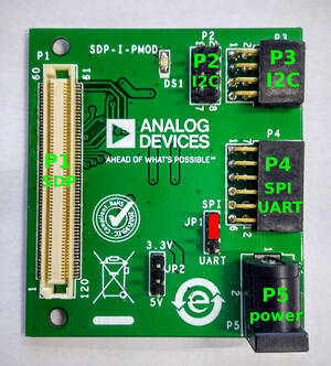
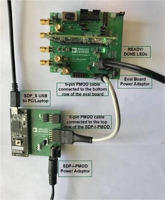
Figure 9 Complete Evaluation Setup with SDP-S and SDP-I-PMOD
ADMX100X General Description
The ADMX100X module is an ultra-low distortion and low noise autonomous digitally controller sinewave signal generator, generating the purest sinusoidal differential signals in its class by exploiting a digital pre-distortion (DPD) algorithm, which is a patented method for sensing and correcting its own output. The difference between ADMX1001 and ADMX1002 is that ADMX1001 has the added capability of acquiring signal as shown on the simplified block diagram.
Source Channel
Both the ADMX1001 and ADMX1002 offer a multi-tone frequency range of up to 40 kHz. The ADMX100X can perform the digital pre-distortion (DPD) algorithm to provide an ultra-low distortion and low noise signal from 30Hz to 20kHz. The module generates an ultra-low distortion performance up to −130dB at 1 kHz with DPD, and −118dB at 1 kHz without DPD. The ADMX100X module has the capability to perform in DC, dual tone, and arbitrary waveform generation mode.
For applications that require different voltage and current levels, the sense lines can be connected to an external buffer or level-shifting circuitry to permit the entire forward signal chain to be corrected.
The module is configurable through a flexible digital interface allows for easy integration into any system. In addition, ATE control bus lines are available for maximum control of the signal in timing-critical applications.
Acquisition Channel
The ADMX1001 module offers an acquisition channel input, which can be accessed using the secondary ADC interface to read the conversion data directly.
ADMX1001 can act as master or slave when supporting coherent test signal generation and offers an auxiliary ADC input, operating at 256 ksps.
The highly integrated data acquisition solution provides 7 programmable gain options with a maximum input range of ±7.5V differential and a maximum input common mode range of ±7V. A 4th order anti-aliasing filter provides rejection up to −130dB. The total dynamic range of the acquisition channel is up to 128dB with a −115dB typical THD with a 1kHz input tone at full scale.
Operation Modes
Single Tone Generation
ADMX100X module is specially designed to generate an ultra-high purity sine waveform from 30 Hz up to 20 kHz by a patented digital pre-distortion (DPD) algorithm method. In addition, the module can generate high-purity signals up to 40kHz without DPD.
Default Mode (without DPD)
This is the default mode when a new frequency and/or amplitude is loaded into the register, and the generate register or trigger pin is toggled. The ADMX100X module performance exceeds the native performance of the components due to its architecture. This is the operation mode for arbitrary waveform generation as well.
With DPD Mode
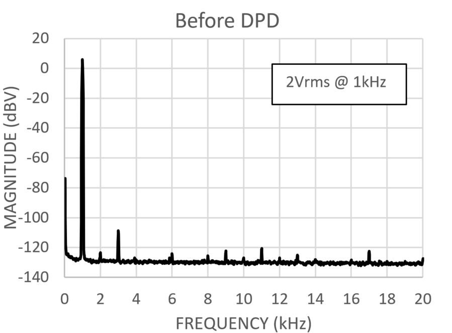
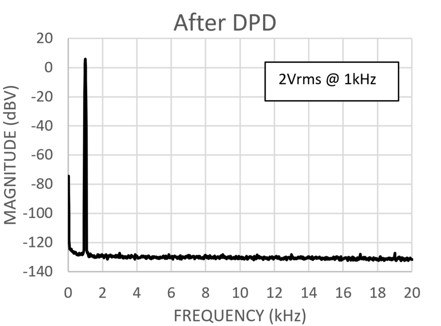
If ultra-high performance is needed the digital pre-distortion (DPD) algorithm can be enabled by software or hardware. The DPD process requires no external reference inputs and exploits a patented differential temporal and amplitude sensing method. When combined with our novel DSP algorithm, this eliminates the electrical measurement errors that would normally limit the performance. The DPD algorithm range frequency goes from 30Hz up to 20kHz, with an amplitude range of up to 3.62VRMS. The figures below show the ADMX100X module THD before and after DPD, as well as the FFT of an ADMX100X module at 1kHz with 2Vrms before and after DPD.
Sense Connection
The DPD algorithm of ADMX100X requires the sense inputs to be connected to the output of ADMX1001 and ADMX1002 which will be used in the process routine of ADMX1001 and ADMX1002 to generate an ultra-high purity sine waveform. The sense connection can be used to combine a user buffer circuit as part of the signal generation in the DPD process by connecting the sense input to the output of the user’s buffer stage.

DC Generation
ADMX100X is capable of generating differential DC output signals up to 11.3V DC between Vp and Vn. The output level can be adjusted in 1µV resolution steps, and the software will verify if the entered parameters are valid by using the valid register. The DC output will be continuously generated after the run command is received and can be stopped by sending a stop command.
Dual-tone Waveform Generation
Two sine wave tones can be generated from 30Hz to 20kHz. The dual-tone waveform generation can be performed in burst mode or continuous mode. The dual-tone waveform frequency resolution can be programmed with 1 µHz resolution while the amplitudes can be programmed with 1 µV resolution.
Arbitrary Waveform Generation
An arbitrary waveform can be programmed by the user. The AWG signal can be programmed up to 20s long and will be stored in volatile memory. Continuous AWG generation can be performed by looping back the waveform stored in memory. ADMX100X contains a 27kHz low pass filter on its output allowing AWG waveforms to be generated within this band. Signals generated in the band will be within a 5% tolerance.
Acquisition Channel
The highly integrated data acquisition solution provides 7 programmable gain options with a maximum input range of ±7.5V differential and a maximum input common mode range of ±7V. A 4th order anti-aliasing filter provides rejection up to −130dB. The total dynamic range of the acquisition channel is up to 128dB with a −115dB typical THD with a 1kHz input tone at full scale.
SPI Control
An overview of the SPI control mode features is as follows:
Standard SPI Mode 3 interface for register access, where the ADC always behaves as an SPI slave.
Indication of a new conversion via the DRDY pin output.
A second method allows the user to merge the ready signal within the DOUT output stream, which allows a reduction in the number of lines across an isolation barrier.
Reading back conversions can be performed by writing 8 bits to address the ADC register and reading back the result from the register.
Continuous readback mode, which is enabled via an SPI write. There is no need to supply the 8 bits to address the ADC_DATA register (Register 0x2C). Data readback occurs on the application of SCLK. The DRDY pin indicates that a conversion result is complete and can be used to trigger a readback of the conversion result.
In continuous read-back mode, there is the option to append either the 8-bit status header or an 8-bit CRC check, or both.
Additional Features
Burst/Continuous Mode
In burst mode, the tone will only be generated for a defined length of time while in continuous mode the waveforms will be generated continuously until the STOP command is sent.
Profiles
Once a digital pre-distortion (DPD) algorithm is used for a given frequency or amplitude, the DPD parameters can be saved into the non-volatile profile memory. If you change the parameters of your signal without storing the previous DPD parameters, these parameters will be lost once a new frequency or amplitude is loaded into the module. When generating a new combination of frequency and amplitude (also known as a profile) DPD algorithm can be performed to generate a high-purity signal and can be stored to be later recalled. Up to 16 such signals can be stored and can be recalled easily by hardware or software. This allows fast-high purity frequency switching. Profiles 1 through 15 can store any signal type (single tone, single tone with DPD, DC, dual tone, etc.), but profile 16 is reserved for an AWG signal type only.
ADMX100X Limitations
The DPD algorithm cannot be used for frequencies above 20 kHz.
The DPD algorithm does not work with signals lower than 100mVrms.
Frequencies above 40 kHz cannot be selected.
Amplitude above 3.5Vrms cannot be set.
Only voltages below 3.5Vrms can be set for frequencies less than 10.5 kHz.
Voltages above 2.5Vrms cannot be set for frequencies greater than 15.5 kHz.
Voltages above 2Vrms cannot be set for frequencies greater than 20.5 kHz.
Only voltages below 1Vrms can be set for frequencies greater than 20.5 kHz
GUI Overview
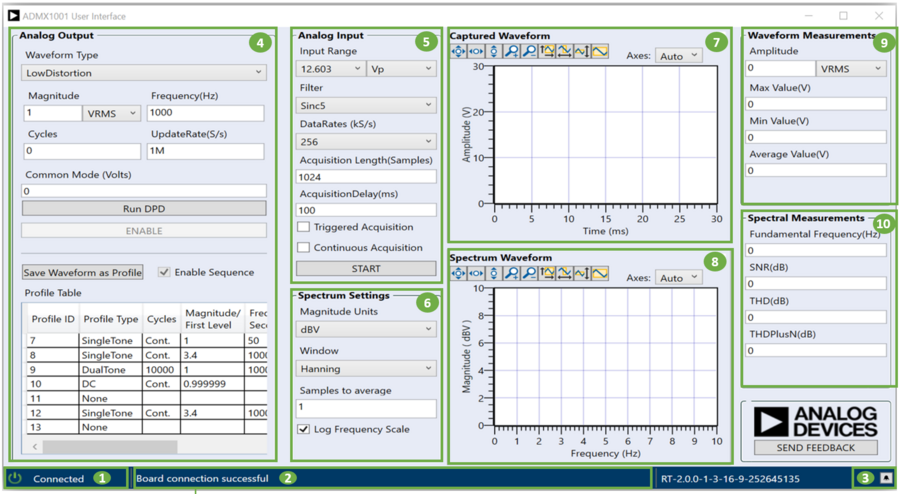
The ADMX100X GUI contains the following components:
Connect/Disconnect button: Click to connect the eval board to the PC.
Status Bar: Displays certain relevant errors/statuses.
Bell icon: Button to show/hide the message panel. Continue to ADMX100X GUI Message Panel for additional details.
Analog Output Panel: Configure parameters and control the source waveform.
Analog Input Panel: Configure parameters and control the acquisition channel (ADMX1001 only).
Spectrum Settings: Configure parameters for the Spectral Waveform displayed (ADMX1001 only).
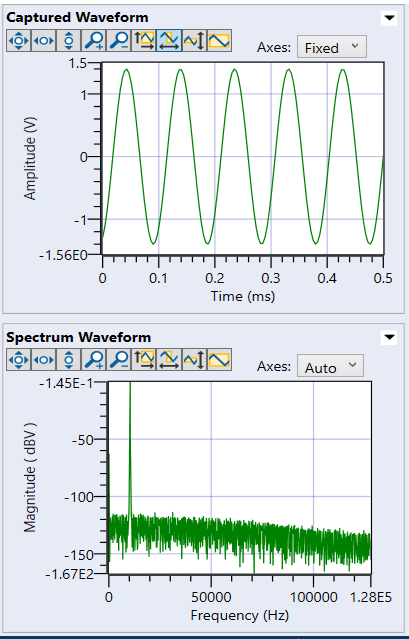
Captured Waveform: Time domain plot of the samples captured by the acquisition channel (ADMX1001 only).
Spectrum Waveform: Frequency domain plot of the FFT of the samples captured by the acquisition channel (ADMX1001 only).
Waveform Measurements: Time domain measurements are calculated using the samples captured by the acquisition channel (ADMX1001 only).
Spectral Measurements: Frequency domain measurements calculated using the FFT of the samples captured by the acquisition channel (ADMX1001 only).
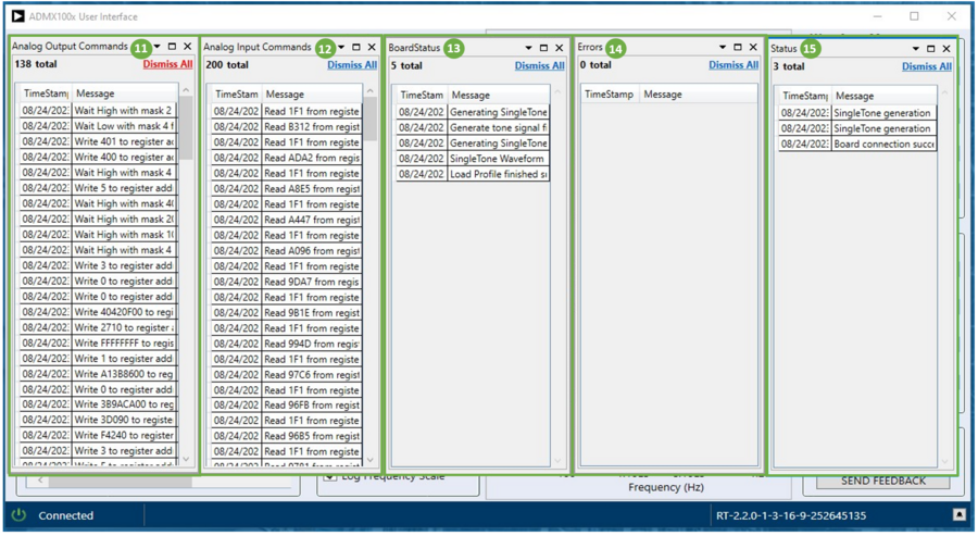
After clicking on the Bell icon in the bottom right of the ADMX100X GUI Status Panel, several message windows can be viewed. These windows contain the following components:
Analog Output Commands: Contains a comprehensive list of SPI commands sent to the source registers of the ADMX100X module.
Analog Input Commands: Contains a comprehensive list of SPI commands sent to the acquisition registers of the ADMX1001 module. This is not used when evaluating the ADMX1002 module.
Board Status: Periodically updated list of the current condition of the board.
Errors: List of errors thrown during operation of the GUI. Generated parameters will then be displayed in the Generated Parameters Panel.
Status: List of statuses updated during operation.
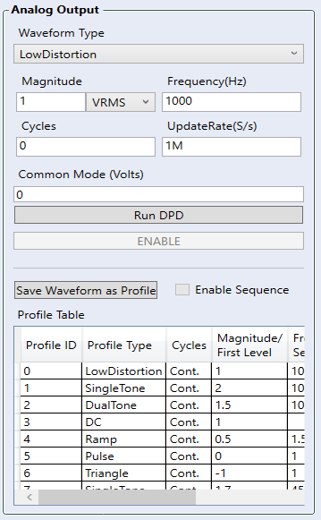
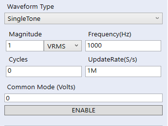
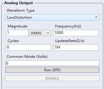
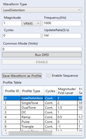
Analog Output Panel
The UI elements present in the Analog Output Panel are as follows:
Enable/Disable: This button starts/stops the signal.
Run DPD: This button runs the digital pre-distortion(DPD), or calibration, algorithm.
Cycles: Use this to change the selection to either “Continuous” (Cycles = 0) or “Single-shot” (1 to 1000000 cycles).
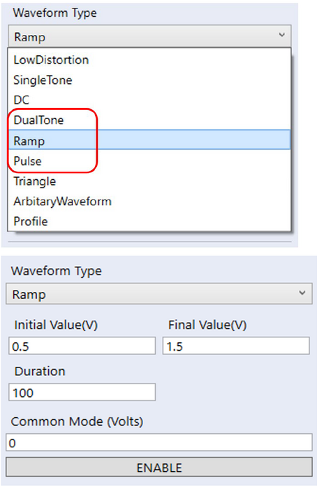
Waveform Type: Use this to change the selection to either “Single-Tone”, “DualTone”, “LowDistortion”, “DC”, “Pulse”, “Ramp”, “Triangle”, “AWG” or “Pulse”.
Common Mode [3]: This field is used to set the common mode offset voltage of the signal to be generated.
Save Waveform as Profile: Saves current waveform in the profile table.
Profile Table: Displays all the saved profiles and their parameters.
Enable Sequencing [4]: Enables running a set of profiles in a user-selected sequence.
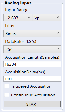
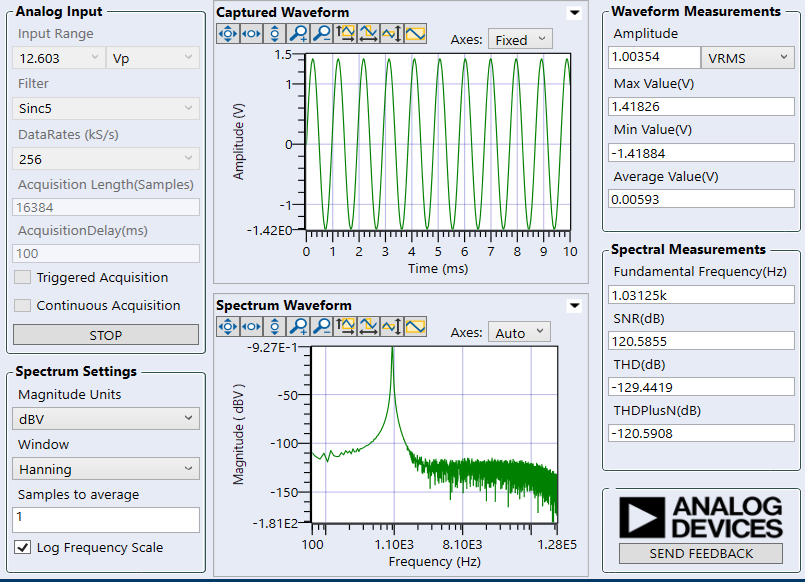
ADMX100X GUI Analog Input Panel
The UI elements present in the Analog Input Panel, are as follows:
Input Range: Provides a drop-down menu to set the range of the input ADC by varying its gain. The input range of the ADC can be changed from 8.912 Vrms to 0.139 Vrms.
Filter: A dropdown menu provides the user a choice between the filter to be used by the acquisition IC to process the ADC samples. The options include “Sinc5”, “Sinc3” and “Wideband”.
DataRate(KS/s): The rate at which the acquisition data is acquired, in kilo-Samples per second.
Acquisition Length: Number of continuous samples to be acquired from the ADC during acquisition.
Acquisition Delay: Amount of delay before acquisition starts.
Continuous Acquisition: This button enables continuous acquisition of the signal. The GUI will keep acquiring newer samples until the STOP button is pressed.
Triggered Acquisition: This button enables triggered acquisition of the signal. The acquisition will start from a positive zero-crossing for each set of samples.
Start/Stop – Starts/Stops the sample acquisition.
ADMX100X GUI Waveform Plot Options (Captured and Spectrum)
The plots to display the acquired data, have the following elements:
Captured waveform Graph: Displays the captured samples vs. time to show the captured waveform to the user.
Spectrum waveform graph: Displays the frequency-domain plot of the acquired samples using signal-to-spectrum domain transforms.
Waveform Graph control panel: This control panel can be used to scale the graph as needed.
Waveform Graph Axes: The Axes dropdown has two options “Auto” and “Fixed”. If we use “Fixed” axes we can manually set the limits of the graph by clicking on the numbers at the edge of the graph and typing in the required value of the axis limit. The “Auto” setting will automatically scale the axes to fit the waveform in the window.
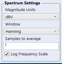
ADMX1001 GUI Spectrum Settings
The settings available for the Spectrum waveform are as follows:
Magnitude Units: Dropdown menu to decide the magnitude units of the spectral magnitude on the y-axis of the spectrum waveform.
Window: Specifies the type of windowing to be used on the input time-domain signal before transforming it to the frequency-domain using FFT.
Samples to average: Specifies the number of sets of samples to average for the spectrum calculation. Only applicable when the “Continuous acquisition” checkbox in the Analog Input Panel is checked, or else the value in this textbox is ignored.
Log frequency scale: The checkbox determines the scale of the Frequency axis (X-Axis). If the checkbox is checked the frequency scale is logarithmic, if the box is kept unchecked the frequency scale is linear.
ADMX1001 GUI Spectrum and Waveform Measurements
The measurements calculated for the time domain (waveform) and frequency domain (spectral) plots are as follows:
Amplitude: Amplitude of the acquired signal.
Max Value: Maximum value in the acquired signal.
Min Value: Minimum value of the acquired signal.
Average Value: Average value of the acquired signal.
Fundamental Frequency: Fundamental frequency of the input signal.
SNR: Signal to Noise Ratio of the signal.
THD: Total harmonic distortion of the signal.
THDPlusN: Total harmonic distortion and noise of the input signal.

Generate a Single-tone without Digital Pre-Distortion (DPD)
To generate a single-tone signal without the DPD algorithm set the “Waveform Type” field to “SingleTone”.
Set the parameters of the waveform according to your requirements. For additional detail on each parameter hover over the input field to see the tooltip.
The cycles parameter can be used to shift the signal generation between “Single-Shot” and “Continuous” (cycles = 0) mode.
Click on the “ENABLE” button to generate the signal. If the signal is in “Single-Shot” mode, the enable button should be clickable right after signal generation is completed. For a signal generation in “Continuous” mode, press the “DISABLE” button, which will appear once the board is ready to start generating the signal, to disable the waveform.
Generate a Single-tone with Digital Pre-Distortion (DPD)
To generate a single-tone waveform calibrated with the DPD algorithm, set the “Waveform Type” field to “LowDistortion”.
Set the parameters of the waveform according to your requirements. For additional detail on each parameter hover over the input field to see the tooltip.
Click on the ‘Run DPD’ button, the status bar should show the message ‘Calibration is running’ and the ‘Run DPD’ button will appear greyed out.
Wait for the “ENABLE” button to become clickable after the message “Calibration successful” displays in the status bar. This process may take up to 2 minutes. If the “Run DPD” button becomes clickable again and the status message shows “Calibration failed”, try to run the calibration again by clicking on “Run DPD”.
Click on the “ENABLE” button to enable the calibrated signal generation.
Note that any change in parameters would require running calibration again. Calibrated signals can be stored in a profile to eliminate having to run calibration in the future for the same set of parameters, see the Storing Profiles section for instructions.
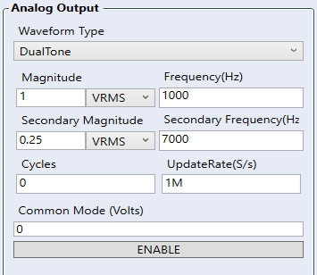
Generate a Dual-tone Signal
The following sequence shall produce a two-tone signal:
Change the “Waveform Type” to DualTone.
Set the appropriate parameters and click the “ENABLE” button.
Click on the “DISABLE” button to disable the generation if needed.
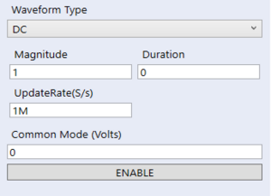
Generate DC Level Generation
The following sequence shall produce a DC signal:
Select the “Waveform Type” DC Level from the drop-down menu.
Set the appropriate parameters for the signal.
Start the signal generation by clicking on the “ENABLE” button.
Click on the “DISABLE” button to disable the generation.
Generate a Triangle, Ramp, or Pulse Waveform
The ADMX100X GUI comes with 3 built-in AWG waveform options for signal generation - a Triangle, a Ramp, or a Pulse signal. Any of these can be generated by performing the following sequence:
Select “Triangle”, “Ramp”, or “Pulse” from the “Waveform Type” drop-down menu.
Set the appropriate parameters for the signal.
Start the signal generation by clicking on the “ENABLE” button.
Click on the ‘DISABLE’ button to disable the generation.
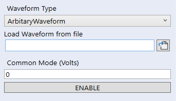
Generate Arbitrary Waveform
The following sequence shall produce an arbitrary waveform:
Select the “ArbitraryWaveform” from the Waveform Type dropdown menu.
Select an input file using the browse option or add the path to an input file in the text box labeled “Load waveform from file”. The format of the input file expected is a list of voltage values with each value on a new line.
Start the signal generation by clicking on the “ENABLE” button.
Click on the ‘DISABLE’ button to disable the generation if needed.
Storing Profiles
Perform the following sequence to save a waveform to a profile:
Select a waveform profile to save by using the “Waveform Type” drop-down menu and selecting any waveform type, except “Profile”.
Set the appropriate parameters of the selected waveform type.
Click on any empty or non-empty profile in the profile table to select it. If selecting a non-empty profile, the previously saved profile table will be overwritten by the new profile.
After selecting the profile ID and the waveform parameters, click on the “Save Waveform as profile” button. This might take up to 2 minutes for a “LowDistortion” waveform.
If the profile is saved successfully, you will be able to see it in the profile table at the selected location.
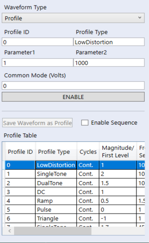
Load and Enable Profiles Without Sequencing
The following sequence shall load the previously saved profile:
Disable any running signal and use the “Waveform Type” dropdown menu to select “Profile” as the waveform type.
Ensure that the “Enable Sequence” button is unchecked.
Click on any profile in the profile table you want to load that is currently not “None”.
The profile selected should show up and populate the “Profile ID”, “Profile Type”, “Param1” and “Param2” fields.
To load and enable the selected profile, click on the “ENABLE” button.
To stop the profile signal generation, click on “DISABLE”.
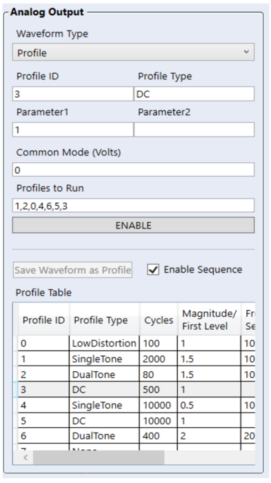
Load and Enable Profiles With Sequencing
The following sequence shall load the previously saved profile with sequencing:
Disable any running signal and use the “Waveform Type” dropdown menu to select “Profile” as the waveform type.
Ensure that the “Enable Sequence” button is checked.
Click on any profile in the profile table you want to add to the sequence that is currently not “None” and is not saved in the “Continuous” mode (has Cycles not equal to 0).
Alternately, you can type the sequence you want to run in the “Profiles to Run” field. If the “Enable” button is not greyed out the sequenced profiles are valid.
Click on the “Enable” button to run the selected sequence.
To stop the profile signal generation, click on “Disable”.
Acquisition
The “Analog Input” panel is used to set the parameters for acquisition.
Set the parameters in the Analog input window, for the description of each parameter, hover over the text field or the drop-down menu to see the tooltip.
The “Triggered Acquisition” checkbox can be checked to enable triggered acquisition.
The “Continuous Acquisition” checkbox can be checked to enable continuous acquisition.
Click the “START” button in the Analog input panel. This will start the acquisition.
Use the “Spectrum Settings” panel to change the scale of the axes of the spectrum graph.
Click on the “Stop” button to stop the acquisition.
Custom Bin Selection
The number of bins used for the fundamental, harmonics, and other components in AC performance calculations, such as SNR, THD, and THD+N, can be adjusted. This flexibility of bin selection can help reduce the effect of spectral leakage, improving AC performance accuracy, particularly when analyzing noise and harmonic distortion.
To do this, go to the GUI folder (C:\Analog Devices\Admx100xEvaluationSoftware-Rel2.3.0\GUI), open SpectrumSettings.json, and adjust the number of bins as necessary.
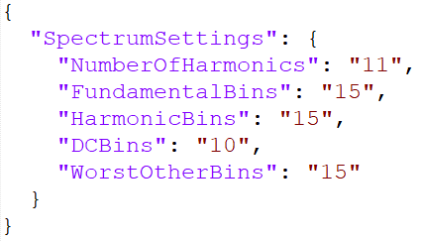
After saving the spectrum settings, run the Acquisition channel to apply the changes, and it should reflect to the updated AC performance.
Applications Information
ATE Control Interface
The Automatic Test Equipment (ATE) control interface can be used to provide a simple protocol for initiating an instruction to perform a DPD calibration or signal generation by driving and monitoring pins on the module. The test parameters, like the amplitude and frequency of the signal, must still be loaded through SPI.
Test Sequence
There are two possible test sequences: Signal Generation & DPD Calibration. It is not necessary to run a DPD calibration phase before every signal generation sequence. The following examples use all the module’s ATE control pins. However, the user can choose to use none, only the TRIG line, or more depending on the level of control required.
Signal Generation
The procedure below should be followed for stimulus generation:
Turn-on power supplies to modules (+3.3V & +/-9V).
Set Enable (EN) High - Enables internal supplies within the module.
Wait until module initialization has completed (READY=1).
Load serial test configuration data.
Low to high TRIG transition initiates the test sequence.
Module outputs synchronization (SYNC_OUT) pulses over the period the VALID signal is held high.
Low to High transition of the VALID signal indicates the start of the stimulus.
High to Low transition of the VALID signal indicates the end of the stimulus.
The same test can be run multiple times without reloading the configuration by repeating steps 5 through 8. Once new test configuration data has been reloaded via SPI, the new configuration will need to be revalidated before signal generation can resume without error.
Calibration
To achieve the highest signal purity, a DPD calibration phase must be run at least once before generating an output signal. The DPD calibration data is normally stored in volatile memory and therefore must be re-run after every power supply sequence or once there is a change in the amplitude, frequency, and common-mode voltage settings.
The procedure below should be followed for calibration:
Enable power supplies to modules (+3.3V & +/-9V).
Set Enable (EN) High - Enables internal supplies within the module.
Wait until module initialization has completed (READY=1).
Load serial test configuration data.
Set CAL signal High to start module DPD Calibration procedure.
Monitor the high to low transition of the VALID signal to indicate the end of calibration.
Start generating an output signal.
Coherent Sampling
Coherent sampling describes the sampling of a periodic signal, where an integer number of its cycles fit into a predefined sampling window. This technique is very useful to get the best achievable results when evaluating the dynamic performance of analog-to-digital converters (ADCs). To facilitate coherent sampling, the module can synchronize its signal generation to an external clock by doing the following:
Connect the SYNC_Mode pin to GND by inserting a jumper in the 2-3 position of P12.
Connect the SYNC_IN pin to the SMA input by inserting a jumper in the 2-3 position of P13.
Apply a 100 MHz external clock to J7 to synchronize the generated signal to the external clock.
Notes:
The external clock must be turned on first before applying power to the EVAL-ADMX100X-FMCZ.
Take note of the logic level limits below for the SYNC_IN and SYNC_OUT pins.
Trigger needs to be set high to start generating the signal.
During Coherent Sampling, SYNC_IN must have a 100 MHz clock frequency with a 50% duty cycle.
Although less common, coherent sampling may also be performed by synchronizing the analyzer from the clock generated from the module (SYNC_OUT).