AD7124 Console Application
Supported Hardware
Supported Devices:
Supported Evaluation Boards:
Supported Carrier Boards:
Introduction
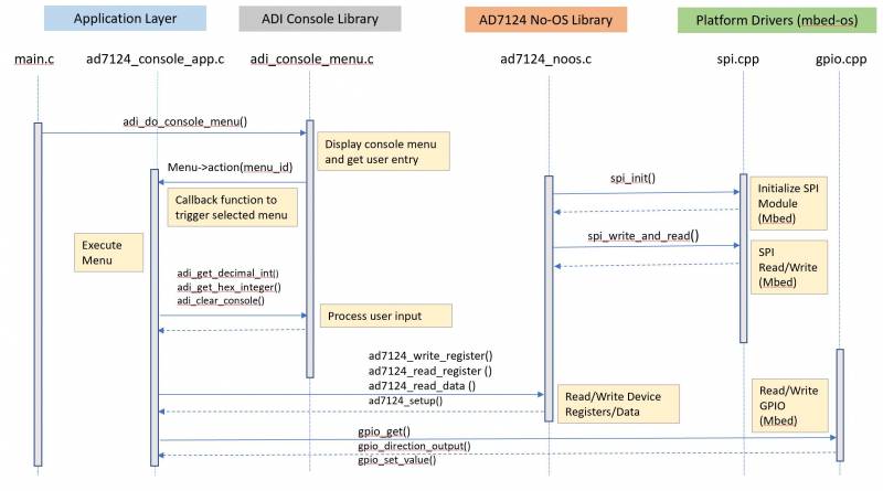
This page gives an overview of using the AD7124 Firmware Example with SDP-K1 EVAL board and AD7124 EVAL board. The firmware example comprises 3 layers of software (from top to bottom): Console Application Layer, Device No-OS Layer and Platform Drivers layer. It support STM32 platform
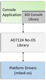
The application layer uses the ADI Console Libraries to create console based User Interactive (UI). The middle layer of No-OS device library have device specific APIs to interface with AD7124 device. These APIs allows direct access to device register map in order to read/write device registers. The bottom layer of Platform Drivers is responsible for Low Level Interface. The platform drivers uses underlying libraries to access low level peripheral (like GPIOs, SPI, I2C, etc).
The Platform simplifies the overall software development process by providing the low level driver support. This reduces the hardware dependency on any STM32 board can be used with same firmware with little modifications (precisely changing a pin mapping).
Interface Diagram
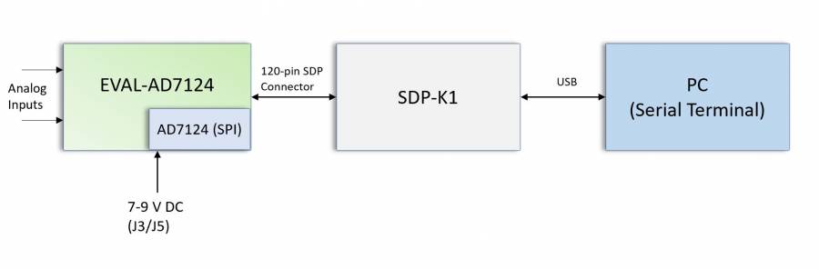
The AD7124-EVAL board is connected to SDP-K1 through 120-pin SDP Connector. The AD7124-EVAL board has external connector to connect up-to 8 analog inputs. The board needs to be powered-up through 9-12V external DC supply. The SDP-K1 is connected to PC through USB cable. The firmware can be loaded into SDP-K1 board through this USB interface from PC. The SDP-K1 acts as a Serial Device and firmware loaded into it interacts with any serial terminal (like Teraterm, Putty, Coolterm, etc) by configuring terminal for proper serial settings (COM Port, Baud Rate, etc).
Useful Links
Note
Linux and HDL are not used in emebdded IIO firmware projects but they may be of interest if you require Linux and/or FPGA support.
Hardware Connections
Power Supply and USB Connection
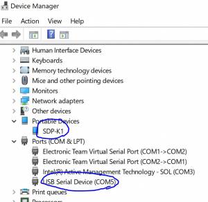
A 7V to 9V DC supply (barrel jack, center pin positive) is required to power the EVAL-AD7124-8SDZ evaluation board. SDP-K1 is powered through USB connection to PC. SDP-K1 acts as a Serial device when connected to PC, which creates a COM Port to connect to Serial Terminals like Teraterm, Putty, etc. The COM port assigned to a device can be seen through the device manager for windows based OS.
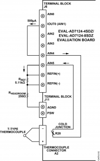
Analog Inputs
The screw terminal connections to J6 and J11 can be used to connect appropriate analog input signals to provide test stimulus to the AD7124.
The AD7124 device can be software configured to interface with external devices (e.g. sensors). The AD7124 Firmware example provides such 2 configurations (selected through console UI) as described below:
Configuration A:
AIN0/AIN1 are used for channel 0, simple voltage measurement
Configuration B:
AIN2/AIN3 go to the A2 thermocouple connector on the evaluation board, and are captured on channel 0. This uses an internal reference and has a bias voltage enabled on AIN2. A suitable thermocouple should be connected to A2 for this measurement. AIN4/AIN5 are an RTD1000 measurement on channel 1. Excitation is provided from AIN1 for this. This requires an external RTD and reference resistor connected as show in the figure below.
Temperature sensing application using AD7124 can be found here
AD7124 Firmware
This section briefs on the usage of firmware. This also explains the steps to compile and build the application using STM32CubeIDE build.
The software execution sequence for the AD7124 Firmware Example is shown below. This is a blocking application as it waits for user input over serial interface (UART). The input is scanned and processed through ‘adi console libraries’. The menu functionality is executed from ad7124_conole_app.c file. The application layer talks with No-OS layer for device registers and data access. The No-OS layer interfaces with Platform Drivers layer for accessing low level peripherals. As name suggests, this layer is platform dependent. AD7124 firmware uses Mbed libraries within Platform Drivers layer. AD7124 Firmware Example is shown below.
Build Guide
Build Prerequisites
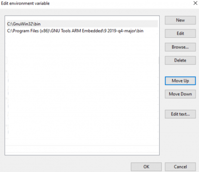
Prior to building a firmware project, it is required to set up an environment so that the build process may find the necessary tools (compiler, linker, SDK etc.). Use the following steps to prepare your environment for building firmware projects for respective platform.
Clone Precision Converters Firmware repository with the –recursive flag:
git clone --recursive https://github.com/analogdevicesinc/precision-converters-firmware
If however you’ve already cloned the repository without the –recursive flag, you may initialize all the submodules in an existing cloned repo with:
git submodule update --recursive --init
Install STM32CubeIDE
Install STM32CubeMX
Building a project
Once the build enviornment is setup, follow the guide below to build your project and generate executable file (.bin/.hex)
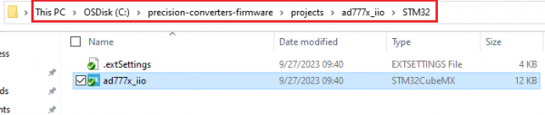
Open the respective project directory by navigating into the “precision_converters_firmware/projects/” folder.
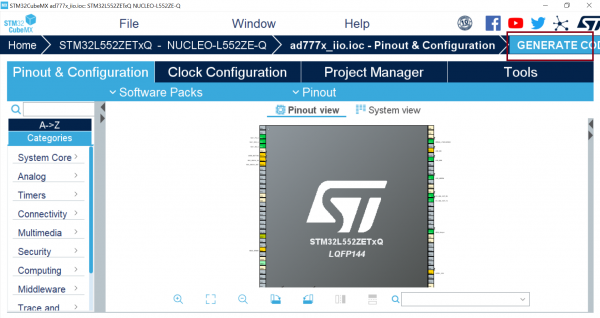
In the “STM32” folder present within the project directory, double click and open the .ioc file present within.
Click on the “Generate Code” option seen on the top right corner
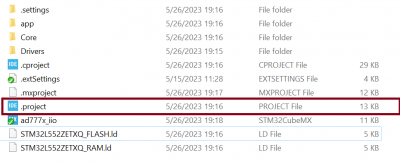
Upon successful generation of drivers for the selected MCU, the autogenerated files would be seen in the same directory where the .ioc file was present. Double click and open the “.project” file seen in the list of files
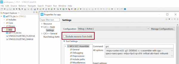
After the project is loaded to the STM32CubeIDE, unfold the adxxxx_iio project seen in the project explorer, right click the “app” folder, select “Settings” under the “C/C++ Build” section on the left pane and un-check the “Exclude resources from build” checkbox. This would ensure that the project specific files are included by the build system
Add compiler flags “-u _printf_float” to the project settings.
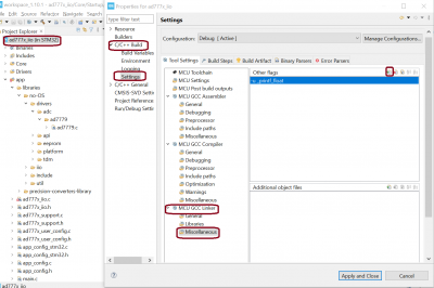
Exclude the generated file syscalls.c from the build process

- To generate the binary file, right click on the adxxxx_iio project seen in the project explorer and select “Properties”, select “Settings” under the “C/C++ Build” section on the left pane, select “MCU Post build outputs” under “Tool Settings” section and check the “Convert to binary file (-O binary)” checkbox.

Build the project by right-clicking on the adxxxx_iio project seen in the project explorer and select “Build Project”

Running a project
Once the firmware build is successful and binary file is generated, copy the generated binary into USB drive hosted by your MCU board (e.g. USB drive hosted by MCU board on windows). This will flash the binary file into MCU present on the controller board. Programming might vary based on the tools used for building a project. The ‘Project Build’ section above talks about this exception at the end of all build steps.
Quick Start
If you have some familiarity with the STM32 platform, the following is a basic list of steps required to start running the code, see below for more detail:
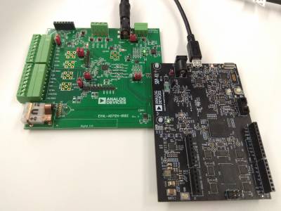
Connect the AD7124 EVAL-board to the SDP-K1 controller board.
Connect the SDP-K1 controller board to your computer over USB.
Follow the steps mentioned in the Build Guide section above.
- Start up a serial terminal emulator (e.g. Tera Term)
Find the com-port your controller board is connected on and select it.
Set the baud-rate for 230400
Reset the controller board and connect.
Use the menu provided over the terminal window to access the evaluation board.
Using the Firmware
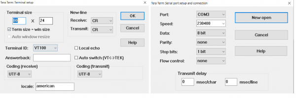
The AD7124 firmware example is configured to have following serial settings:
Baud rate: 230400 Data bits: 8-bits Parity: None Stop bits: 1
Configure your serial terminal (Tera Term) for below settings:
The AD7124 Main menu looks like below (with Tera Term):
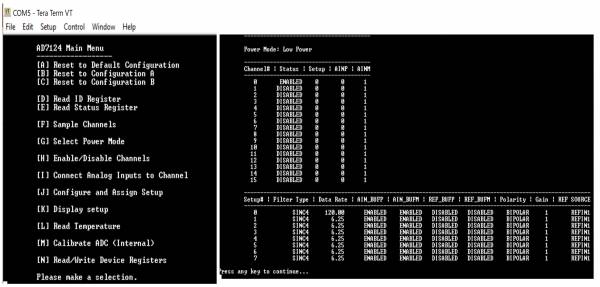
The firmware is designed to be intuitive to use, and requires little explanation, simply enter a number corresponding to the required command and follow the on-screen prompts.
The console menu application provides the following main features:
Enable/Disable individual ADC channel (0-15).
Connect analog input pins to individual channel.
Configure the device setup (0-7) and assign to individual channel (0-15).
Display device and channel setup.
Perform internal device calibration.
Read die temperature (using internal temperature sensor).
Read/Write device registers.
Support
Feel free to ask questions in the EngineerZone