

HDL Support for AD9361 TDD Mode
Using the AD9361 RF Agile Transceiver in TDD (Time Division Duplex) mode, the user has multiple solutions to control the time period of the receive and transmit bursts. The internal enable state machine of device (ENSM) can either be controlled by SPI writes or ENABLE/TXNRX pins. SPI control is considered asynchronous to the DATA_CLK because the SPI_CLK can be derived from a different clock reference and still function properly. The SPI control ENSM method is recommended when real time control of the synthesizers is not necessary. SPI control can be used for real time control as long as the Base Band Processor (BBP) has the ability to perform timed SPI writes accurately.
The ENABLE/TXNRX pin control method is recommended if the BBP has extra control outputs that can be controlled in real time, allowing a simple two-wire interface to control the state of the AD9361 device. This user guide intend to provide an in-depth description about the HDL support of the ENABLE/TXNRX pin control method.
ENABLE/TXNRX Pin Control
In TDD, the state of the TXNRX pin controls whether the AD9361 will transition from ALERT to Rx or ALERT to Tx. If TXNRX is high, the device will move into the Tx state. If TXNRX is low, the device will move into the Rx state. The TXNRX pin level should be set during the ALERT state. The logic level of TXNRX must not change during the Rx, Tx, or FDD states. The role of the ENABLE pin is to transition the ENSM state to the next state, and can be operated in pulse mode or level mode.
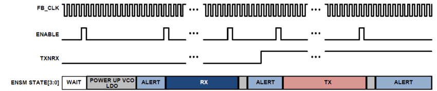
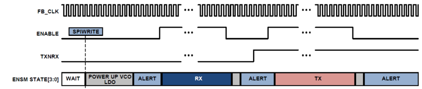
By default the ENABLE and TXNRX pins are controlled by GPIO’s. This solution similarly to the SPI write ENSM control, can not provide a real time control of these pins.
The axi_ad9361 IP core has an integrated TDD controller, which gives the possibility to control the ENABLE/TXNRX pins in real time. The TDD controller consists of a counter, which counts on every positive edge of the FB_CLK, and a several software accessible registers, which defines the time when the ENABLE and TXNRX pins should be set or reset.
TDD Controller
In the block diagram below can be seen the axi_ad9361 IP core with the integrated TDD controller modules inside. If the controller is enabled, all the data flow from or to the device will be controlled by this module.

The AXI register map of the TDD controller, and the description of each registers can be found under the following link: TDD REGISTER MAP
The foundation of the TDD controller is a counter, which can be configured to count until a specified frame length. The maximum value of the counter can be defined by simple divide the desired frame length with the current FB_CLK clock period, e.g. in the case of a 10 ms frame length, when the FB_CLK is 122.88 Mhz the value of the REG_TDD_FRAME_LENGTH register must be 1228800.
After defining the frame length, the user can define one or two sets of pointers, which will tell the exact location, when the device will start/stop a receive/transmit burst inside a frame.
Start and stop a receive burst consists of the following action points, each point will define a pointer:
Enabling the RX synthesizer
Enabling the RX RF path inside the device (ALERT to RX state transition)
Enabling the RX Data path inside the FPGA (the core starts to get valid data from the devices interface)
Disabling the RX Data path inside the FPGA
Disabling the RX RF path inside the device (RX to ALERT state transition)
Disabling the RX synthesizer
Start or stop a transmit burst consists of the following action points, each point will define a pointer:
Enabling the TX synthesizer
Enabling the TX RF path inside the device (ALERT to TX state transition)
Enabling the TX Data path inside the FPGA (the core starts to push valid data to the devices interface)
Disabling the TX Data path inside the FPGA
Disabling the TX RF path inside the device (TX to ALERT state transition)
Disabling the TX synthesizer
After enabling the TDD controller, the counter starts to count and compares its value to the values of the pointers, if there is a match the corresponding control signal is asserted. Using this simple method the controller generates six different control signals: VCO_RX_EN, VCO_TX_EN, RF_RX_EN, RF_TX_EN, TX_DP_EN, RX_DP_EN. Using these control signals the TDD interface module will drive the ENABLE and TXNRX pins accordingly.
Register Map
Address |
Reg Name |
|||||
|---|---|---|---|---|---|---|
HDL |
DWORD |
BITS |
Field Name |
Type |
Default Value |
Description |
0x10 |
0x40 |
TDD_CONTROL_0 |
TDD Control & Status |
|||
[5] |
TDD_GATED_TX_DMAPATH |
RW |
0x0 |
If this bit is set, the core requests data from the TX DMA, just when the data path is active. Otherwise will requests continuously on the adjusted rate. The purpose of this feature is to facilitate debug. This bit must be SET to preserve data integrity. |
||
[4] |
TDD_GATED_RX_DMAPATH |
RW |
0x0 |
If this bit is set, the core provides data for the RX DMA, just when the data path is active. Otherwise will provides continuously on the adjusted rate. The purpose of this feature is to facilitate debug. This bit must be SET to preserve data integrity. |
||
[3] |
TDD_TXONLY |
RW |
0x0 |
If this bit is set- the TDD controller ignores all the TX_* timing registers below and assumes continuous receive operation within a frame. |
||
[2] |
TDD_RXONLY |
RW |
0x0 |
If this bit is set- the TDD controller ignores all the RX_* timing registers below and assumes continuous transmit operation within a frame. |
||
[1] |
TDD_SECONDARY |
RW |
0x0 |
Enable the secondary transmit/receive on the active frame. If this bit is clear - the controller only uses the _1 timing registers below. If this bit is set - the controller uses the _1 and _2 timing registers below. |
||
[0] |
TDD_ENABLE |
RW |
0x0 |
If set, enables the TDD controller- software must set this bit after programming all the registers that controls the tdd timing. Any device settings needs to be done (for example bring the AD9361 to the alert state) prior to to setting this bit. The controller keeps the frame counters in reset if this bit is reset. A 0 to 1 transition in this bit starts the frame counter and tdd mode of operation. |
||
0x11 |
0x44 |
TDD_CONTROL_1 |
TDD Control & Status |
|||
[7:0] |
TDD_BURST_COUNT |
RW |
0x00 |
If set to 0x0 and enabled (TDD_ENABLE is set) - the controller operates in TDD mode as long as the TDD_ENABLE bit is set. If set to a non-zero value, the controller operates for the set number of frames and stops. |
||
0x12 |
0x48 |
TDD_CONTROL_2 |
TDD Control & Status |
|||
[23:0] |
TDD_COUNTER_INIT |
RW |
0x000000 |
The controller sets the frame counter to this value when starting TDD operation. This is the starting offset value for the TDD frame counter. |
||
0x13 |
0x4c |
TDD_FRAME_LENGTH |
TDD Control & Status |
|||
[23:0] |
TDD_FRAME_LENGTH |
RW |
0x000000 |
The frame length is the terminal count for the 10ms counter running at the digital interface clock- as an example for a 245.76MHz clock it is 0x258000. |
||
0x14 |
0x50 |
TDD_SYNC_TERMINAL_TYPE |
TDD Control & Status |
|||
[0] |
TDD_SYNC_TERMINAL_TYPE |
RW |
0x0 |
Set this bit, if the current terminal will generate the syncronization pulse, reset otherwise. |
||
0x18 |
0x60 |
TDD_STATUS |
TDD Control & Status |
|||
[0] |
TDD_RXTX_VCO_OVERLAP |
RO |
0x0 |
This bit is asserted, if exist a time interval when both the TX and RX VCOs are powered up. |
||
[1] |
TDD_RXTX_RF_OVERLAP |
RO |
0x0 |
This bit is asserted, if exist a time interval when both the TX and RX RF datapath are powered up. |
||
0x20 |
0x80 |
TDD_VCO_RX_ON_1 |
TDD Control & Status |
|||
[23:0] |
TDD_VCO_RX_ON_1 |
RW |
0x000000 |
Defines the offset (from frame count equal zero), when the RX VCO powers up at the first time. The controller enables the receive VCO, when the frame count reaches this value. The VCO may have to be enabled before data can be received. The user needs to make sure, that the RF device is in a state, from where this operation is valid. |
||
0x21 |
0x84 |
TDD_VCO_RX_OFF_1 |
TDD Control & Status |
|||
[23:0] |
TDD_VCO_RX_OFF_1 |
RW |
0x000000 |
Defines the offset (from frame count equal zero), when the RX VCO powers down at the first time. The controller disables the receive VCO, when the frame count reaches this value. The user needs to make sure, that the RF device is in a state, from where this operation is valid. |
||
0x22 |
0x88 |
TDD_VCO_TX_ON_1 |
TDD Control & Status |
|||
[23:0] |
TDD_VCO_TX_ON_1 |
RW |
0x000000 |
Defines the offset (from frame count equal zero), when the TX VCO powers up at the first time. The controller enables the transmit VCO, when the frame count reaches this value. The user needs to make sure, that the RF device is in a state, from where this operation is valid. |
||
0x23 |
0x8c |
TDD_VCO_TX_OFF_1 |
TDD Control & Status |
|||
[23:0] |
TDD_VCO_TX_OFF_1 |
RW |
0x000000 |
Defines the offset (from frame count equal zero), when the TX VCO powers down at the first time. The controller disables the transmit VCO when the frame count reaches this value. The user needs to make sure, that the RF device is in a state, from where this operation is valid. |
||
0x24 |
0x90 |
TDD_RX_ON_1 |
TDD Control & Status |
|||
[23:0] |
TDD_RX_ON_1 |
RW |
0x000000 |
Defines the offset (from frame count equal zero), when the RX data path is activated at the first time. The controller enables the receive chain when the frame count reaches this value. The user needs to make sure, that the RF device is in a state, from where this operation is valid. |
||
0x25 |
0x94 |
TDD_RX_OFF_1 |
TDD Control & Status |
|||
[23:0] |
TDD_RX_OFF_1 |
RW |
0x000000 |
Defines the offset (from frame count equal zero), when the RX data path is deactivated the first time. The controller disables the receive chain when the frame count reaches this value. The user needs to make sure, that the RF device is in a state, from where this operation is valid. |
||
0x26 |
0x98 |
TDD_TX_ON_1 |
TDD Control & Status |
|||
[23:0] |
TDD_TX_ON_1 |
RW |
0x000000 |
Defines the offset (from frame count equal zero), when the TX data path is activated at the first time. The controller enables the transmit chain, when the frame count reaches this value. This register and the TX_DP_ON register controls the delay between the data path being activated and the time to actually push the transmit data through the transmit chain in the device. |
||
0x27 |
0x9c |
TDD_TX_OFF_1 |
TDD Control & Status |
|||
[23:0] |
TDD_TX_OFF_1 |
RW |
0x000000 |
Defines the offset (from frame count equal zero), when the TX data path is deactivated at the first time. The controller disables the transmit chain, when the frame count reaches this value. This register and the TX_DP_OFF register controls the delay between the data path being deactivated and the time to actually stop transmitting data through the transmit chain in the device. |
||
0x28 |
0xa0 |
TDD_RX_DP_ON_1 |
TDD Control & Status |
|||
[23:0] |
TDD_RX_DP_ON_1 |
RW |
0x000000 |
Defines the offset (from frame count equal zero), when the controller starts to accept data from the digital interface for receive. |
||
0x29 |
0xa4 |
TDD_RX_DP_OFF_1 |
TDD Control & Status |
|||
[23:0] |
TDD_RX_DP_OFF_1 |
RW |
0x000000 |
Defines the offset (from frame count equal zero), when the controller stops to accept data from the digital interface for receive. |
||
0x2a |
0xa8 |
TDD_TX_DP_ON_1 |
TDD Control & Status |
|||
[23:0] |
TDD_TX_DP_ON_1 |
RW |
0x000000 |
Defines the offset (from frame count equal zero), when the controller starts to request data from the system memory for transmit. The data rate is controlled by the TDD controller. |
||
0x2b |
0xac |
TDD_TX_DP_OFF_1 |
TDD Control & Status |
|||
[23:0] |
TDD_TX_DP_OFF_1 |
RW |
0x000000 |
Defines the offset (from frame count equal zero), when the controller stop requesting data from the system memory for transmit. |
||
0x30 |
0xc0 |
TDD_VCO_RX_ON_2 |
TDD Control & Status |
|||
[23:0] |
TDD_VCO_RX_ON_2 |
RW |
0x000000 |
The secondary pointer for VCO_RX_ON. |
||
0x31 |
0xc4 |
TDD_VCO_RX_OFF_2 |
TDD Control & Status |
|||
[23:0] |
TDD_VCO_RX_OFF_2 |
RW |
0x000000 |
The secondary pointer for VCO_RX_OFF. |
||
0x32 |
0xc8 |
TDD_VCO_TX_ON_2 |
TDD Control & Status |
|||
[23:0] |
TDD_VCO_TX_ON_2 |
RW |
0x000000 |
The secondary pointer for VCO_TX_ON. |
||
0x33 |
0xcc |
TDD_VCO_TX_OFF_2 |
TDD Control & Status |
|||
[23:0] |
TDD_VCO_TX_OFF_2 |
RW |
0x000000 |
The secondary pointer for VCO_TX_OFF. |
||
0x34 |
0xd0 |
TDD_RX_ON_2 |
TDD Control & Status |
|||
[23:0] |
TDD_RX_ON_2 |
RW |
0x000000 |
The secondary pointer for RX_ON. |
||
0x35 |
0xd4 |
TDD_RX_OFF_2 |
TDD Control & Status |
|||
[23:0] |
TDD_RX_OFF_2 |
RW |
0x000000 |
The secondary pointer for RX_OFF. |
||
0x36 |
0xd8 |
TDD_TX_ON_2 |
TDD Control & Status |
|||
[23:0] |
TDD_TX_ON_2 |
RW |
0x000000 |
The secondary pointer for TX_ON. |
||
0x37 |
0xdc |
TDD_TX_OFF_2 |
TDD Control & Status |
|||
[23:0] |
TDD_TX_OFF_2 |
RW |
0x000000 |
The secondary pointer for TX_OFF. |
||
0x38 |
0xe0 |
TDD_RX_DP_ON_2 |
TDD Control & Status |
|||
[23:0] |
TDD_RX_DP_ON_2 |
RW |
0x000000 |
The secondary pointer for RX_DP_ON. |
||
0x39 |
0xe4 |
TDD_RX_DP_OFF_2 |
TDD Control & Status |
|||
[23:0] |
TDD_RX_DP_OFF_2 |
RW |
0x000000 |
The secondary pointer for RX_DP_OFF. |
||
0x3a |
0xe8 |
TDD_TX_DP_ON_2 |
TDD Control & Status |
|||
[23:0] |
TDD_TX_DP_ON_2 |
RW |
0x000000 |
The secondary pointer for TX_DP_ON. |
||
0x3b |
0xec |
TDD_TX_DP_OFF_2 |
TDD Control & Status |
|||
[23:0] |
TDD_TX_DP_OFF_2 |
RW |
0x000000 |
The secondary pointer for TX_DP_OFF. |
||
Synchronization
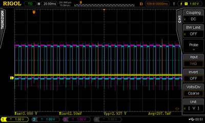
To test and validate the functionality of the TDD controller, two Avnet PicoZed SDR Development Kits were used, in conjunction with the Avnet AES-PZSDRCC-FMC-G carrier board and the AD-PZSDR2400TDD-EB RF personality card.
TDD systems are using the same frequency channel for both Uplink (UL) and Downlink (DL) transmission, but in different times. This scheme gives the possibility to dynamically allocate the amount of time for UL and DL, resulting an asymmetric UL/DL transmission. To prevent unwanted interference of different transmission links between nodes, a network synchronization is required between base stations and users. In practice this synchronization can be obtained by using IEEE 1588 or GPS.
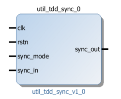
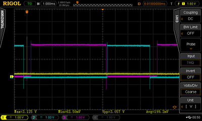
In our case, the goal was to showcase the TDD support of the AD9361, so the synchronization of the two devices is solved as simple as possible, without using any of the above mentioned method. The reference design contains a pulse generator core (util_tdd_sync), which is independent of the axi_ad9361 core, and can be generate a small pulse in a defined time interval. Than this pulse will be fed into both axi_ad9361 core and will reset the counter, this way the two controller will stay synced.
Important
This reference design will not provide a complete solution for the network synchronization.
Parameters of util_tdd_sync
Name |
Default |
Description |
|---|---|---|
|
100000000 |
Relative time between two synchronization pulse. The actual time is the
value multiplied by the |
IO Ports of util_tdd_sync
Name |
Type |
Description |
|---|---|---|
|
Clock |
It’s driven by the system clock (S_AXI_ACLK), which is a 100 Mhz clock signal. |
|
Reset |
Active low reset, driven by the system reset. (S_AXI_RSTN) |
|
Input |
If |
|
Input |
External input signal, which comes from the other terminal. |
|
Output |
This pin is connected to the |
To activate the sync pulse generator the software needs to set the
REG_TDD_SYNC_TERMINAL_TYPE register to 0x01.
TDD_SYNC Interface IO Mapping
Carrier Name |
Connector Name |
Port Name |
FPGA IO Pin |
|---|---|---|---|
AES-PZSDRCC-FMC-G |
PMOD1 / P11 |
PMOD1[5] |
W19 |
PMOD1 / J58 |
PMOD1_5_LS |
AA20 |
Linux Driver
Example Platform Device Initialization
The TDD HDL core driver is a platform driver and can currently only be instantiated via devicetree.
Required devicetree properties:
compatible: Should always be"adi,axi-tdd-1.00"reg: Base address and register area size. This parameter expects a register range.adi,profile-config0: At least one (maximum 7) configuration profile should be defined. A profile contains the values of the registers: COUNTER_2 (0x8048), FRAME_LENGTH (0x804c), SYNC_TERM_TYPE (0x8050), VCO_RX_ON_1 (0x8080), VCO_RX_OFF_1 (0x8084), VCO_TX_ON_1 (0x8088), VCO_TX_OFF_1 (0x808C), RX_ON_1 (0x8090), RX_OFF_1 (0x8094), TX_ON_1 (0x8098), TX_OFF_1 (0x809C), TX_DP_ON_1 (0x80A0), TX_DP_OFF_1 (0x80A4), RX_DP_ON_1 (0x80A8), RX_DP_OFF_1 (0x80AC).
cf_ad9361_tdd_core_0: cf-ad9361-tdd-core-lpc@79028000 {
    compatible = "adi,axi-tdd-1.00";
    reg = <0x79028000 0x1000>;
    adi,profile-config0 = <0 1228800 1 1198080 771920 771920 1198080 39832 771536 781032 1197696 44832 766536 786032 1192696>; /* Master Configuration Profile */
    adi,profile-config1 = <0 1228800 0 771920 1198080 1198080 771920 781032 1197696 39832 771536 786032 1192696 44832 766536>; /* Slave Configuration Profile */
};
Device Attributes
/sys/bus/iio/devices/iio:device5$
ls -l
-rw-rw-rw- 1 root root 4096 Jan  1  1970 burst_count
-rw-rw-rw- 1 root root 4096 Jan  1  1970 dev
-rw-rw-rw- 1 root root 4096 Jan  1  1970 dma_gateing_mode
-rw-rw-rw- 1 root root 4096 Jan  1  1970 dma_gateing_mode_available
-rw-rw-rw- 1 root root 4096 Sep 21 09:11 enable
-rw-rw-rw- 1 root root 4096 Jan  1  1970 enable_mode
-rw-rw-rw- 1 root root 4096 Jan  1  1970 enable_mode_available
-rw-rw-rw- 1 root root 4096 Jan  1  1970 name
lrwxrwxrwx 1 root root    0 Sep 21 09:10 of_node -> ../../../../../firmware/devicetree/base/fpga-axi@0/cf-ad9361-tdd-core-lpc@79028000
drwxrwxrwx 2 root root    0 Jan  1  1970 power
-rw-rw-rw- 1 root root 4096 Jan  1  1970 profile_config
lrwxrwxrwx 1 root root    0 Sep 21 09:10 subsystem -> ../../../../../bus/iio
-rw-rw-rw- 1 root root 4096 Jan  1  1970 uevent
The following attributes are implemented:
Show Device Name
/sys/bus/iio/devices/iio:device5$
cat name
cf-ad9361-tdd-core-lpc
Enable the TDD Controller
/sys/bus/iio/devices/iio:device5$
echo 1 > enable
Choose the Desired Configuration Profile
/sys/bus/iio/devices/iio:device5$
echo 1 > profile_config
Configure the DMA Gate
/sys/bus/iio/devices/iio:device5$
cat dma_gateing_mode_available
none rx_only tx_only rx_tx
/sys/bus/iio/devices/iio:device5$
echo none > dma_gateing_mode
Configure the RX/TX Mode
/sys/bus/iio/devices/iio:device5$
cat enable_mode_available
rx_tx rx_only tx_only
/sys/bus/iio/devices/iio:device5$
echo rx_tx > enable_mode
Support
If you have any question related to the HDL or the AD-PZSDR2400TDD-EBZ board please visit the Help and support section for more information.