

TEST-CAPI-SELFTEST HDL project
The test_capi_selftest project is a self-contained verification design. It does not target an evaluation board and it does not talk to any external device. Instead, it instantiates the peripheral controllers that a software platform layer has to drive - SPI, UART, I2C, timer and GPIO - both in the Processing System (PS) and in the Programmable Logic (PL), and loops each one of them back onto itself inside the FPGA.
Because every transmitter is wired to its own receiver, software running on the carrier can write a pattern through a peripheral, read it back through the same peripheral and decide whether the driver - and the C API (CAPI) layer underneath it - behaves as expected. No cables, no jumpers and no daughter board are required, which makes the design usable for automated regression runs.
The interfaces exercised by the design are:
Interface |
PS instance |
PL instance |
|---|---|---|
SPI |
SPI0 (EMIO), MOSI looped to MISO |
|
UART |
UART1 (EMIO), TX looped to RX |
|
I2C |
I2C0 (EMIO) |
|
Timer |
TTC0 |
|
GPIO |
EMIO GPIO, bit 9 looped to bit 8 through the fabric |
|
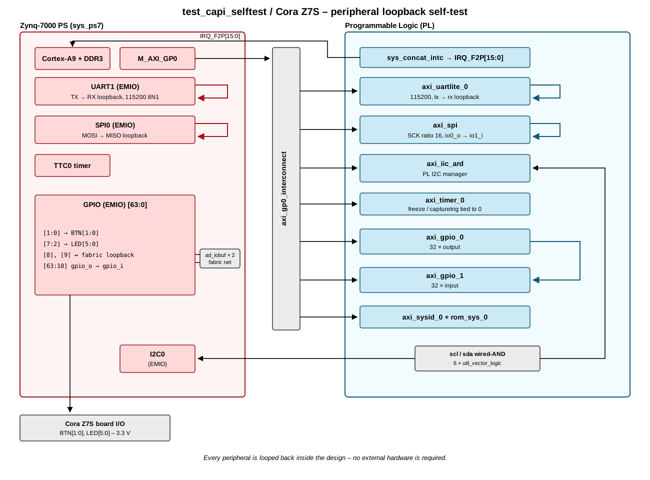
The two I2C managers are the exception to the one-peripheral-one-loopback rule: they are tied together on a single emulated open-drain bus, so a transfer started by one manager is observed by the other. The design contains no I2C subordinate.
Supported boards
None. The design is fully self-contained and requires no evaluation board.
Supported devices
None.
Supported carriers
Evaluation board |
Carrier |
FMC slot |
|---|---|---|
- |
- |
The Arduino shield headers of the Cora Z7S are not used by this project; the only pins constrained at the top level are the two push buttons and the six LEDs of the carrier. The design was tested in hardware with VIO set to 3.3 V.
Block design
Block diagram
The peripherals and their loopback paths are depicted in the below diagram:
Clock scheme
There is no external clock source and no clock generator in the design. Every
clock comes from the PS PLLs through the FCLK outputs, as configured by the
Cora Z7S base design.
Clock |
Frequency |
Used by |
|---|---|---|
|
100 MHz |
AXI interconnect and every AXI peripheral, plus the
|
|
40 MHz |
not used, the design has no DMA |
Since axi_spi is configured with an SCK ratio of 16, the resulting
PL SPI clock is 6.25 MHz.
CPU/Memory interconnects addresses
The addresses are dependent on the architecture of the FPGA, having an offset added to the base address from HDL (see more at CPU/Memory interconnects addresses).
Instance |
Zynq |
|---|---|
axi_iic_ard* |
0x4160_0000 |
axi_spi |
0x44A0_0000 |
axi_uartlite_0 |
0x44A1_0000 |
axi_timer_0 |
0x44A2_0000 |
axi_gpio_0 |
0x44A3_0000 |
axi_gpio_1 |
0x44A4_0000 |
axi_sysid_0* |
0x4500_0000 |
Legend
* instantiated by the Cora Z7S base design
SPI connections
SPI type |
SPI manager instance |
Loopback |
|---|---|---|
PS |
SPI0 (EMIO) |
|
PL |
|
|
PS SPI1 is enabled on EMIO by the Cora Z7S base design, but this project leaves it unconnected at the top level.
I2C connections
I2C type |
I2C manager instance |
Alias |
I2C subordinate |
|---|---|---|---|
PS |
I2C0 (EMIO) |
- |
none, the bus is shared with the PL manager |
PL |
axi_iic |
|
none, the bus is shared with the PS manager |
The iic_ard interface port created by the Cora Z7S base design is removed,
and the two managers are joined by an open-drain bus model built out of six
util_vector_logic instances (three per line, for scl and sda): each
manager’s output enable and output data are OR-ed to obtain its released/driven
state, and the two results are AND-ed to obtain the wired-AND bus level, which
is then fed back to both managers’ inputs.
UART connections
UART type |
UART instance |
Baud rate |
Loopback |
|---|---|---|---|
PS |
UART1 (EMIO) |
115200 |
|
PL |
|
115200 |
|
Timers
Two timers are available: the PS TTC0, which is re-enabled by this project, and
the PL axi_timer_0. The unused inputs of the latter (freeze,
capturetrig0 and capturetrig1) are tied to 0.
GPIOs
Two independent GPIO paths are provided.
The PL path is a pure register-to-register loopback: axi_gpio_0 is
configured as 32 outputs, axi_gpio_1 as 32 inputs, and the whole 32-bit
output vector is connected to the input vector.
The PS path uses the EMIO GPIO of the sys_ps7 instance, 64 bits wide. Bits
0 to 7 leave the FPGA towards the carrier buttons and LEDs, bits 8 and 9 are
strapped together through a pair of ad_iobuf instances on an internal
fabric net, and the remaining bits are looped back directly from gpio_o to
gpio_i.
GPIO signal |
Direction |
HDL GPIO EMIO |
Software GPIO |
|---|---|---|---|
(from FPGA view) |
Zynq-7000 |
||
BTN0 |
IN |
0 |
54 |
BTN1 |
IN |
1 |
55 |
LED0_B |
OUT |
2 |
56 |
LED0_R |
OUT |
3 |
57 |
LED0_G |
OUT |
4 |
58 |
LED1_B |
OUT |
5 |
59 |
LED1_R |
OUT |
6 |
60 |
LED1_G |
OUT |
7 |
61 |
GPIO loopback receiver |
IN |
8 |
62 |
GPIO loopback driver |
OUT |
9 |
63 |
unused, directly looped back |
- |
10 to 63 |
64 to 117 |
Interrupts
Below are the Programmable Logic interrupts used in this project.
Instance name |
HDL |
Linux Zynq |
Actual Zynq |
|---|---|---|---|
axi_spi |
8 |
52 |
84 |
axi_uartlite_0 |
9 |
53 |
85 |
axi_timer_0 |
10 |
54 |
86 |
axi_iic_ard* |
11 |
55 |
87 |
axi_gpio_0 |
12 |
56 |
88 |
axi_gpio_1 |
13 |
57 |
89 |
Legend
* connected by the Cora Z7S base design
Building the HDL project
The design is built upon ADI’s generic HDL reference design framework. ADI makes the sources available on the HDL repository. To get the source you must clone the HDL repository, and then build the project as follows:
Linux/Cygwin/WSL
Building the Cora Z7S project:
~$
cd hdl/projects/test_capi_selftest/coraz7s
~/hdl/projects/test_capi_selftest/coraz7s$
make
A more comprehensive build guide can be found in the Build an HDL project user guide.
Resources
More information
Support
Analog Devices, Inc. will provide limited online support for anyone using the reference design with ADI components via the EngineerZone FPGA reference designs forum.
For questions regarding the ADI Linux device drivers, device trees, etc. from our Linux GitHub repository, the team will offer support on the EngineerZone Linux software drivers forum.
For questions concerning the ADI No-OS drivers, from our No-OS GitHub repository, the team will offer support on the EngineerZone microcontroller No-OS drivers forum.
It should be noted, that the older the tools’ versions and release branches are, the lower the chances to receive support from ADI engineers.