Hardware Guide
Overview
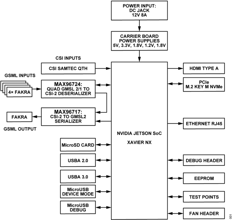
The AD-GMSL522-SL GMSL Carrier Board (also referred as Viper board) is a higher resolution NVIDIA Jetson based carrier board for converting RAW camera data from GMSL cameras/Deserializers into display data.
It is compatible with Maxim deserializer/serializer EV kits and has 4 GMSL inputs and 2 GMSL outputs.
It is a user-friendly GMSL platform for receiving and transmitting data over a GMSL link. The platform enables NPI, demonstrations, customer, and ecosystem development. This platform has hardware interconnects and software tools that enable customers in their development of GMSL.
Carrier Board Feature List
Connection to Jetson Xavier NX
260-pin SO-DIMM connector
GMSL/CSI inputs
SAMTEC – compatible with MAXIM EvKits to CSI inputs of the SOM
4xFakra connectors to MAX96724 GMSL to CSI deserializer
GMSL outputs
MAX96717 CSI to GMSL serializer
USB
USB 2.0 Micro B (device only)
USB 2.0 Micro B (debug)
USB 2.0 Type A
USB 3.0 Type A
Wired Network
Gigabit Ethernet (RJ45 connector)
Display
HDMI™ Type A (v2.0a/b)
M.2 Key M connector
PCIe (Gen4) x4 lane, control
MicroSD Card
UI and indicators
Reset header: power, reset, and force recovery
LEDs: Power
Miscellaneous
Fan connector: 5 V, PWM and tach
Power
DC Jack: 12V, 8A input
Main 5V supply: MAX25206ATPA
Main 3.3V supply: MAX25206ATPA
Main 1.8V, 1.2V, 1V supplies: LTC3303ARUCM
Developer kit operating temperature range
0⁰C to 35⁰C
Power
Power Input
The AD-GMSL522-SL has a single 12 V supply input, distributed to the internal power supplies and interface connectors.
The power adapter to be used with AD-GMSL522-SL needs to have the following specifications:
12 V output, and at least 8 A output current ability.
Mating barrel jack connector dimensions: 2.50 mm ID (0.098“), 5.50 mm OD (0.217”), with positive center pin.
The ADM1177 hot swap controller monitors current and voltage via an on-chip, 12-bit analog-to-digital converter. The ADM1177 charges up the gate of the FET to turn on the load. It continues to charge up the GATE pin until the linear current limit (set to 100 mV/RSENSE) is reached. On this carrier board RSENSE is 0.01Ω which sets the current limit at 10 A. The input voltage and current can be read from this device by accessing it at the 0xB4 I2C address.
Power Supplies
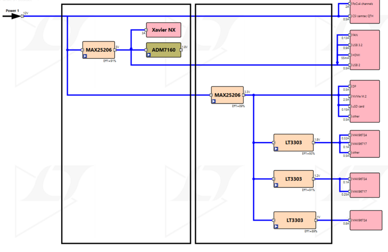
The main DC-DC power supply is a MAX25206ATPA/VY+ converter. This powers up the Xavier NX module and a few other loads on the carrier board. It is designed for 12 V input and 5V, 5A output. The default configuration is for the fixed output version, with the FB pin connected to BIAS. FSYNC and SPS are user configurable by changing the soldering of P22 P23. The Clock Output SYNCOUT outputs 180 degrees out of phase relative to the internal oscillator. In the design, this output is connected to the synchronization inputs of the other supplies, with the option to disconnect it if needed.
The ADM7160 is an 1V8 output LDO used in creating the power sequence needed for the SOM power-up. It powers U45 bus buffer, used to isolate the EN_CR_SUPPLIES signal from SYS_RESET*pin of the SOM.
The 3V3 rail is implemented using another MAX25206ATPA/VY+ but with adjustable output. It is enabled by the SOM after it has POWER_EN high. This can be synchronized with the SYNCOUT of the 5 V supply, or can be user configurable if R236 is desoldered. This will supply various circuits on the board and will serve as the input supply of the converters for the lower rails.
1V0, 1V2 and 1V8 rails are implemented with a LTC3303ARUCM#TRPBF each, the difference is in the feedback resistors used. They are enabled by default by PGOOD_3V3, but if the timing requirements are not met, they can be enabled by the EN_CR_SUPPLIES signal, together with the 3V3 supply. To achieve this R184 should be depopulated and R185 R395 should be populated. These supplies can be synchronized with the main 5 V supply, or have the MODE/SYNC pin conventionally pulled high or low.
If the power-up sequence was successful and the supplies are in the operating range, DS9 will be ON.
All the supplies are monitored by the onboard voltage monitor AD7291BCPZ (U40). The voltages are divided at the input because the device has an on-chip 2.5 V reference. The AD7291 provides a 2-wire serial interface compatible with I2C interfaces and has the following I2C address: 0x2FF
Power Sequence
The power-up sequence is similar to the one implemented in the official NVIDIA Jetson Nano carrier board. The circuit will provide at least 430 ms delay between SHUTDOWN_REQ and POWER_EN.
U38 and U44 are connected to form a SR latch with NAND gates. POWER_EN has 100k pull-down on module, so initial state is always 0.
Jumper on P11 pins 9 and 10 - Auto-power-on enabled
At power-on, both LATCH_SET and LATCH_RESET are pulled-up to VDD_5V_SYS.
Both C287 and C323 are charging, C323 will charge faster resulting in LATCH_RESET HIGH while LATCH_SET LOW => so POWER_EN is enabled, and the SOM is powered on. When C297 charges, LATCH_SET will change state to HIGH, but in this case the output of the latch remembers the previous state so POWER_EN also will keep it state.
If SHUTDOWN_REQ* is pulled low then LATCH_RESET is pulled low so the output will reset and POWER_EN goes low. But since SHUTDOWN_REQ* is not driven during power-up, it will go high again when deasserted but there will be no change on POWER_EN.
If the board is in the state when POWER_EN is HIGH (SET=1) and the user forces shutdown pulling PWR_BTN* low then Q11 will open and LATCH_RESET will be LOW resulting in POWER_EN LOW.
The board will remain off until the power cable is plugged back in again (LATCH_SET is always HIGH as long as VDD_5V_SYS is present)
Jumper on P11 pins 7 and 8 - Auto-power-on disabled
At power on, both LATCH_SET and LATCH_RESET are pulled-up to VDD_5V_SYS. U26 has Hi-Z output until C323 is charged and LATCH_RESET is HIGH. The time constant for C297 is significantly decreased since now R292 and R389 are in parallel so LATCH_SET will be HIGH after 0.011ms while C323 is charging slower, LATCH_RESET is HIGH After ~10 ms. This results in a LOW state for POWER_EN. When PWR_BTN* is pressed, LATCH_SET changes state to 0, resulting in HIGH on POWER_EN
If SHUTDOWN_REQ* is pulled low, then LATCH_RESET is pulled low so the output of the latch is reset to 0 and POWER_EN goes low.
But since SHUTDOWN_REQ* is not driven during power-up, it will go high again so LATCH_RESET=1 and output of U26 becomes active. Now it is possible to power on back the board using the PWR_BTN* signal and not by unplugging the power cable. If pins 1 and 2 of P11 are connected for a short time, at least 50 ms, this will result in LATCH_SET going LOW while LATCH_RESET is HIGH so POWER_EN will go HIGH and the SOM powers on. When releasing the pins 1 and 2 LATCH_SET will be HIGH again, but no change will be seen at the at the output of the latch.
Power over Coax
The AD-GMSL522-SL carrier board is designed to send power as well as data over coax cables, enabling to power remote devices such as automotive cameras without the need for extra wiring or power circuitry.
There is a power over coax (PoC) filter for each GMSL input connector that covers the forward and reverse channel frequency bands.
MAX20087 camera power protector is used to provide protection on the PoC. This is a quad camera protector that delivers 500 mA load current per channel. Each output is individually protected from short and overcurrent conditions.
By default, the 12 V supply that is supposed to power the remote devices is connected to the outputs of the camera power protector with 0 Ohm resistors R401, R403, R407, R405. This will limit the current per channel to 500 mA, but in case more current is needed and the 12 V supply allows this, R402, R404, R408, R406 can be populated instead of R401, R403, R407, R405 and the devices will be powered directly from the 12 V supply without any current limitation, or protection.
Inputs
CSI Inputs-Samtec Connector
A QTH-030-01-L-D-A high speed connector is present on the bottom of the board. GMSL to CSI deserializer EV Kits can be connected here. In the default configuration, if an EvKit is mounted on the carrier board, it will not be supplied by the carrier board. R136, R153, R152 can be soldered on the carrier to connect the Evkit to the power supplies of the AD-GMSL522-SL carrier board.
Important
Please check the board and don’t plug the power supply of the Evkit connected to P1 if R152 is installed!
The GPIO signals from this connector are routed to GPIO pins of Xavier NX which are CMOS – 1.8V Type. Please make sure that the GPIO pins of the Evkit are configured to be supplied by the 1V8 VDDIO.
12 MIPI CSI lanes (CSI0-CSI3) of the XavierNX are routed to this connector, supporting either 4x2, 2x4 CSI-2 DPHY v1.2 configurations.
GMSL (Deserializer)
J1, J2, J3, J4 Fakra connectors(59S2AQ-40MT5-Z_1) on the right side of the board are connected to the inputs of MAX96724GTN/VY+. This provides reliable platform to evaluate the MAX96724 device using standard FAKRA coaxial cables. This deserializer device support high-bandwidth, gigabit multimedia serial links (GMSL-1 or GMSL-2) and offers spread spectrum and full-duplex control channel features.
On-board SERDES
Quad Deserializer
MAX96724GTN/VY+ Quad tunneling GMSL2/1 to CSI-2 deserializer
Port B D-PHY signals of the MAX96724 are routed to MIPI D-PHY inputs of Xavier.
Configuration pins are used to set desired working modes during powerup for the deserializer.
There are two digital I2C configurable potentiometers VR8 and VR1 on the board to set the CFG pin levels. Alternatively, rework the 0 Ω resistors to connect the analog voltage divider and tune the voltage manually. Voltages on CFG pins can be monitored through CFG0 and CFG1 test points (TP27, TP30).
The digital potentiometers in the MAX5419 series are controlled through the I2C signals: MAX96724_CFG_SCL, MAX96724_CFG_SDA.
Address of I2C potentiometers for CFG pins of MAX96724.
The default state of the configuration pins of the MAX96724 set the device into the following state: GMSL-2, 6 Gbps
Tip
If the state of the configuration pins needs to be changed, please refer to the MAX96724 data sheet to see the recommended resistor values to select each configuration.
Single Serializer
MAX96717GTJ/VY+ CSI-2 to GMSL2 serializer
The AD-GMSL522-SL provides a proven design to evaluate the MAX96717 high-bandwidth GMSL serializer with spread spectrum and full-duplex control channel with the use of a standard FAKRA coaxial cable.
The CSI interface of the MAX96717 is connected to MAX9674.
Configuration pins are used to set desired working modes during power-up for the serializer. There are two digital I2C configurable potentiometers VR5 and VR4 on the board to set the CFG pin levels. Alternatively, rework the 0 Ω resistors to connect the analog voltage divider and tune the voltage manually. Voltages on CFG pins can be monitored through CFG0 and CFG1 test points (TP47, TP48).
The digital potentiometers in the MAX5419 series are controlled through the I2C signals: MAX96717_CFG_SCL, MAX96717_CFG_SDA.
Address of I2C potentiometers for CFG pins of MAX96724
Tip
If the state of the configuration pins needs to be changed, please refer to the MAX96717 data sheet to see the recommended resistor values to select each configuration.
Outputs
HDMI
HDMI Type A connector (P10) is directly routed to the HDMI V2.0 interface supported by the Xavier NX module.
GMSL (Serializer)
J7 is the Fakra connector that is tied to the MAX96717 GMSL output pin. It is labeled on the board silkscreen as “OUT MAX96717”. This connection does not support Power-over-Coax due to the fact that the AD-GMSL522-SL board has its own power supply. This does not mean that a deserializer board with Power-over-Coax enabled cannot be connected to this connection. This output can be used to evaluate deserializer designs or to emulate a camera device via sending a colorbar from the deserializer.
Other Interfaces
USB
Jetson Xavier NX supports up to three USB 2.0 ports and a single USB 3.2 port. On AD-GMSL522-SL, the USB interfaces are used as follows:
Ethernet
M1 is a RJ45 Gigabit ethernet connector that has all the necessary magnetics integrated.
MicroSD card
The AD-GMSL522-SL carrier board brings the SDMMC interface from the connector pins for SD card use. P12 is a surface mount, right angle connector, for microSD™ card.
NVMe
The AD-GMSL522-SL board includes an M.2 Key M NVMe Expansion slot (P5). The PCIE signals are routed to PCIE0 interface of the Xavier NX Module. This supports up to Gen4 speed.
Fan Connector
The AD-GMSL522-SL carrier board includes a 4-pin Fan header (P26). This connector is compatible with 70797 Auvidea Cooling Kit.
Reset Header
System signals such as POWER_BTN*, FORCE_RECOVERY*, SYS_RESET*, are brought to a standard 0.254 mm pitch header P11.
Pin |
Signal |
Usage/Description |
1 |
PWR_BTN* |
Connect Pins 1 and 2 to initiate POWER-ON (if AUTO POWER-ON is disabled) |
2 |
GND |
|
3 |
FORCE_RECOVERY* |
Connect Pins 3 and 4 during POWER-ON for USB FORCE RECOVERY MODE |
4 |
GND |
|
5 |
SYS_RESET* |
Temporarily connect Pins 5 and 6 to reset the system |
6 |
GND |
|
7 |
AUTO_PWR_ON |
Jumper on Pins 7 and 8 to disable AUTO POWER-ON |
8 |
LATCH_SET |
|
9 |
Not used |
Jumper on Pins 9 and 10: AUTO POWER-ON is enabled |
10 |
Not used |
Download