Hardware User Guide
Introduction
The AD-SWIOT1L-SL design incorporates the AD74413R Quad-Channel, Software Configurable Input and Output and the MAX14906 Quad-Channel industrial Digital Output/Digital Input ICs, allowing the multiplexing of several analog and digital functions on four channels which can be independently configurable through software to act as:
Voltage Input or Output
Current Input or Output
Digital Input or Output
RTD Measurement
A 10 Mbps single-pair Ethernet link, using the ADIN1110 10BASE-T1L MAC/PHY, enables remote data acquisition and device configuration. The 10BASE-T1L interface can also be used for powering the system via the Single-pair Power over Ethernet (SPoE) technology using the LTC9111 Powered Device (PD) controller. This way power and data for the system are provided over the same cable to simplify the cabling infrastructure and cost significantly.
The system can be powered from an external 24 V supply for applications requiring high current capabilities. Up to 1.2 A can be output on any channel configured as a digital output. The power supply solution also includes the ADP1032 high-performance, isolated micropower management unit (PMU) to provide power and digital control for software-configurable I/O devices in one of the most compact formats. The LT8304 Micropower No-Opto Isolated Flyback Converter together with MAX17671 and ADP223 completes the power tree to provide power to the digital part of the design.
The onboard MAX32650 ultralow power ARM® Cortex®-M4 microprocessor exposes all the necessary debug and programming features to enable a complete software development experience with the system. It is coupled with 1 Gb RAM and 64 Mb Flash external memories to meet the most demanding applications and provide the flexibility to implement any protocol stack. Security features are enabled by the MAXQ1065 security coprocessor. The system’s firmware is based on ADI’s open-source no-OS framework and a user-friendly graphical user interface (GUI) for evaluation and further development.
The figures represented below illustrate the main components used in the AD-SWIOT1L-SL project.
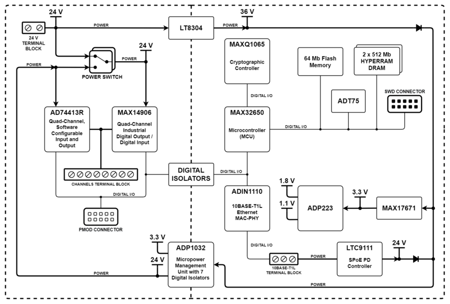
Figure 1 AD-SWIOT1L-SL Simplified Block Diagram
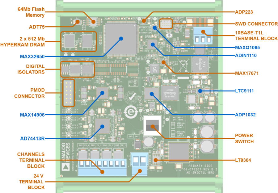
Figure 2 AD-SWIOT1L-SL Development Board
Front-end
In order to obtain a system that is software configurable I/O, the hardware portion which composes the front end of the AD74413R and MAX14906 combination needs to be designed to accommodate all available analog and digital functions.
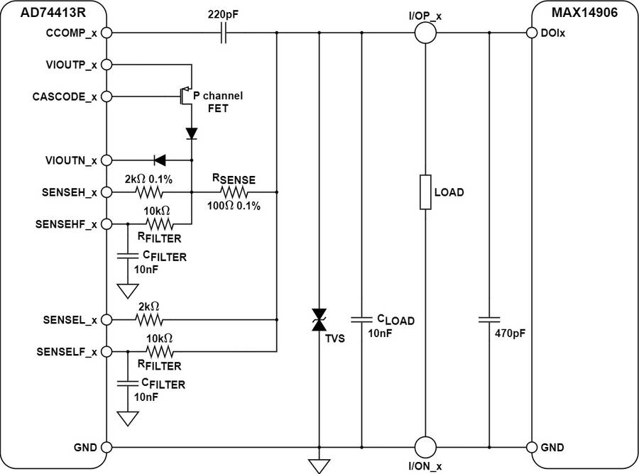
The 220 pF capacitor connected to the CCOMP_x pins allows the AD74413R to drive high capacitive loads in the voltage output use case.
The P channel FET is used to lower power dissipation on the AD74413R die in cases where a low resistive load is present.
The 2 kΩ resistor connected to the SENSEH_x pins is used to close the loop in the current output mode. The low tolerance of this resistor and RSENSE (0.1%) is required to improve accuracy in RTD measurements.
The other 2 kΩ resistor connected to the SENSEL_x pins is also used to close the loop in voltage output mode, besides the current output one.
The RFILTER and CFILTER components connected to the SENSEHF_x and SENSELF_x pins are used to measure the current through the RSENSE or the voltage between the I/OP_x and I/ON_x screw terminals.
The TVS diodes connected on each I/OP_x and I/ON_x screw terminals have the purpose to provide protection against overvoltages (±40 V DC).
The 470 pF capacitors connected to each DOIx pins on the MAX14906 are required for ESD protection.
The LOAD can be any analog or digital industrial device or instrument.
Power Supply Options
The AD-SWIOT1L-SL board can be powered in two ways:
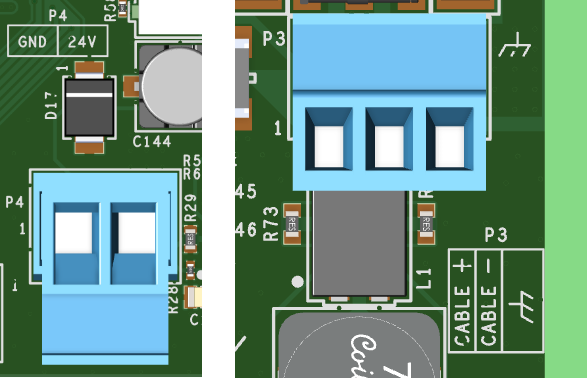
Figure 4 AD-SWIOT1L-SL Power Supply
Power from an external 24 V supply via the “24 V TERMINAL BLOCK”, P4 connector on the board.
Power from an SPoE supply via the “10BASE-T1L TERMINAL BLOCK”, P3 connector on the board.
Each pin function is indicated in a drawing on the PCB board like in the right side picture.
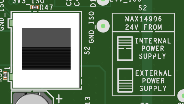
Figure 5 AD-SWIOT1L-SL Power Switch
If both power supplies are in the system simultaneously, the system will take power from the external power supply connected to the “24 V TERMINAL BLOCK”.
The design also includes a “POWER SWITCH” to switch the power (24 V) source. The power source for MAX14906 can the from the ADP1032 internal supply, or from the external power supply.
To quickly identify the “POWER SWITCH” position and meaning, a table is drawn on the PCB board like in the right side picture.
For high-power applications which require the usage of MAX14906 (Industrial Digital I/O) device, the system will need to be powered from an external supply with the “POWER SWITCH” commuted to the external supply position like in the figure represented below.
Note
The greyed-out portions from the figures below represent circuits not used in that particular configuration.
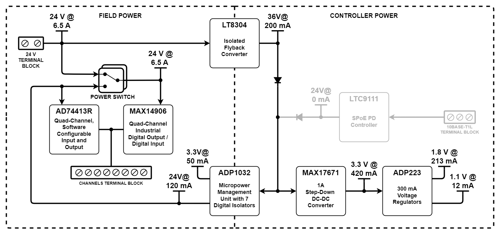
Figure 6 AD-SWIOT1L-SL at Full Power
If the “POWER SWITCH” is commuted to the internal supply position like in the figure represented below, the MAX14906 will not function at full power, such that it will be necessary to take care of how the device is configured.
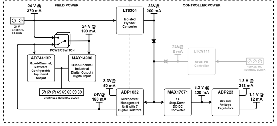
Figure 7 AD-SWIOT1L-SL at Mid Power
If the system is powered from a Single-pair Power over Ethernet (SPoE) supply, like the EVAL-SPoE-KIT-AZ, via the “10BASE-T1L TERMINAL BLOCK”, as is illustrated in the figure below, the MAX14906 will not function at full power, but is still usable depending on the application.
Important
Care should be taken into consideration to flip the “POWER SWITCH” into the internal power supply position to avoid the situation to establish communication with an unpowered device, which may trigger a software crash.
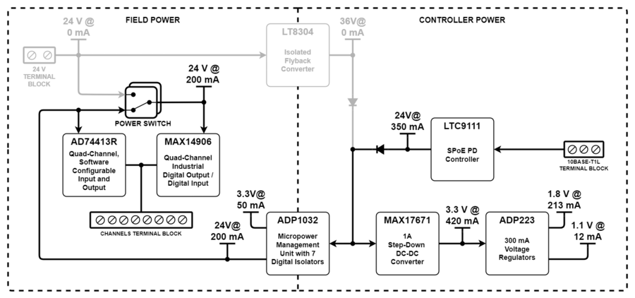
Figure 8 AD-SWIOT1L-SL at Low Power
Power Supply Timing
As described above, the system can be powered in two ways: from the SPoE power supply or the external power supply connector.
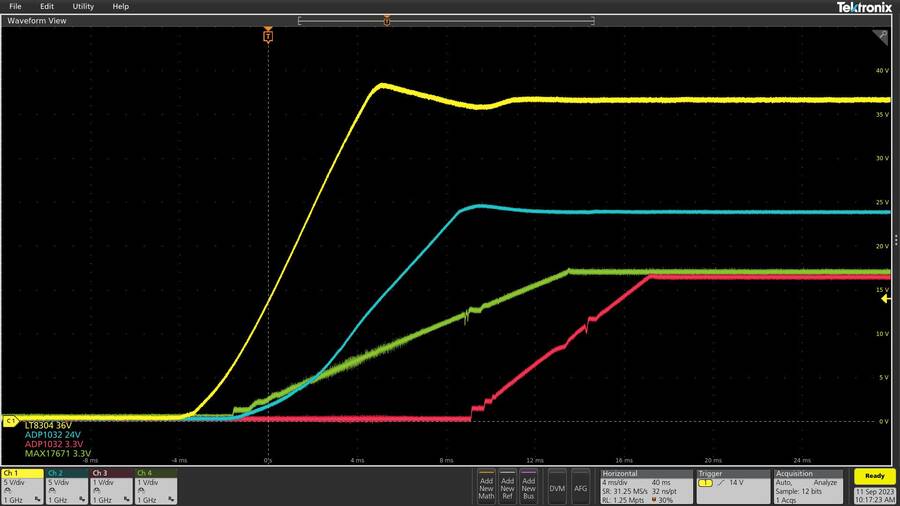
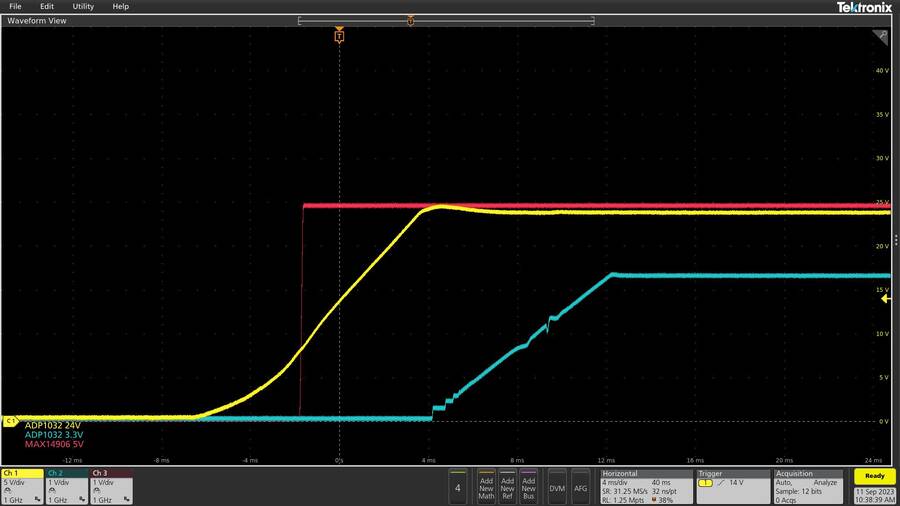
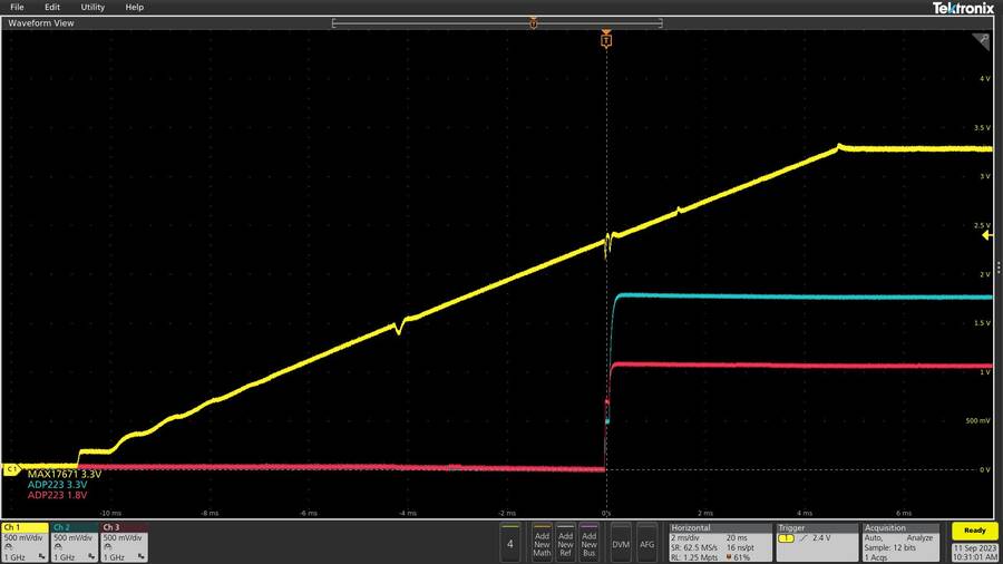
No matter how the system is powered, the primary supply voltage, which can be 24 V or 36 V, will power the main supplies (ADP1032 and MAX17671) for both sections of the system (“FIELD POWER” and “CONTROLLER POWER”) as illustrated above.
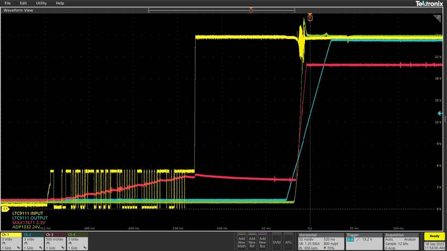
The figures illustrated below represent the power-up sequence for the main supplies (ADP1032 and MAX17671), when the system is powered from the external 24 V power supply (left), and when the system is powered from an SPoE power supply (right).
On the right side illustration, when the system is powered from an SPoE power supply, it can also be observed the Serial Communication Classification Protocol (SCCP) transaction, before the power (24 V) is turned on.
After that, the “CONTROLLER POWER” section will be powered by MAX17671 together with ADP223 (left side illustration) to provide the 3.3 V, 1.8 V, and 1.1 V voltages for the MAX32650 and the rest of the peripherals, including one side of the digital interface.
At the same time, the “FIELD POWER” section is powered by ADP1032 (right side illustration) to provide the 24 V and 3.3 V voltages for AD74413R, MAX14906, and the rest of the peripherals which compose one side of the digital interface.
Protection
On the 24 V external power supply, the AD-SWIOT1L-SL board is protected against surges by a TVS diode.
The MAX14906 is protected against electrostatic discharge (ESD) events by a ceramic capacitor of 470 pF, 100 V on each DOI_ pin and by a ceramic capacitor of 1 μF, 100 V on each VDD_ pin. Also, reverse current protection is provided for MAX14906 by using a P-channel transistor on each VDD_ pin.
Each AD74413R channel is protected against overvoltages (±40 V) via a TVS diode.
On the networking side, the ADIN1110 is protected against surges via ESD suppressors.
The SPoE power supply, composed from LTC9111 circuitry also provides protection against overvoltages (+40 V).
Software I/O Connections
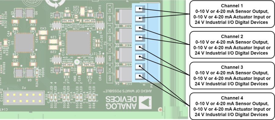
Since this system has 4 channels, which can be configured with different functions, to control or monitor different industrial sensors, actuators, or other devices, to identify pin functions and channel names easily, a drawing is added on the PCB.
The screw terminals tolerate overvoltages up to ± 40 V DC.
The system is designed to be robust in noisy environments and can withstand overvoltage scenarios such as miswire and surge events.
Isolation
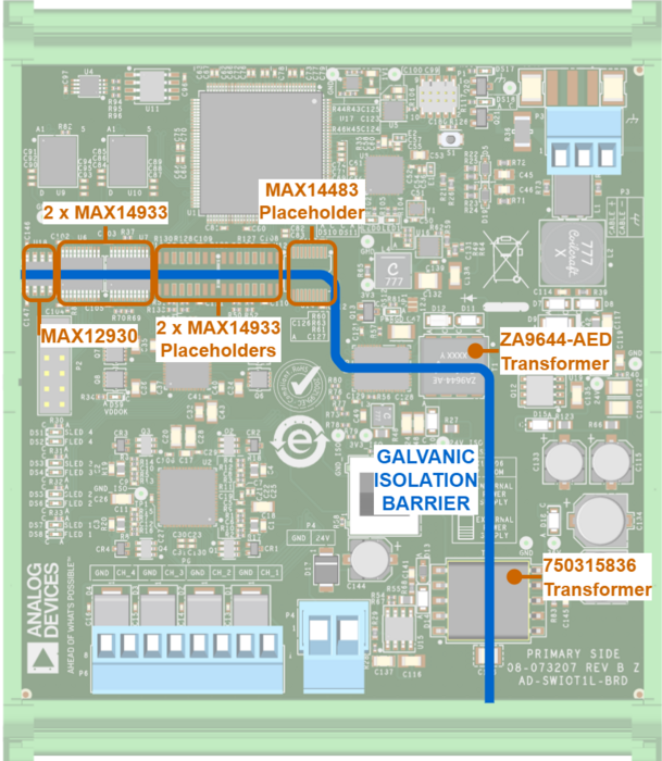
To provide a minimum of safety to the design from eventual energy surges during operation or setup installation, to protect the digital section of the design which contains the MCU (MAX32650) and other sensitive devices, the field devices AD74413R, MAX14906 and the eventual device connected on the PMOD connector are isolated from the rest of the system via digital isolators and isolated power supplies plus a galvanic isolated barrier.
The components used for digital and power isolation on the AD-SWIOT1L-SL board meet the requirements for an industrial application.
For digital isolation the following components are used: MAX12930, MAX14483 and optionally MAX14933 while for power ZA9644-AED and 750315836 transformers and ADP1032 which also provide isolation for some digital signals.
Feature Expansion
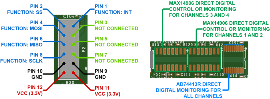
A PMOD connector, P2, is present on the board for feature expansion reasons, in order to extend the platform capabilities. For this, an SPI interface with an additional output signal and power is exposed on the PMOD connector.
There are also placeholders for additional digital isolators (U12, U13, and U14) to enable if necessary direct control or monitoring for all channels without using only the SPI interface. This may be necessary for high-speed process control applications.
10BASE-T1L Interfacing
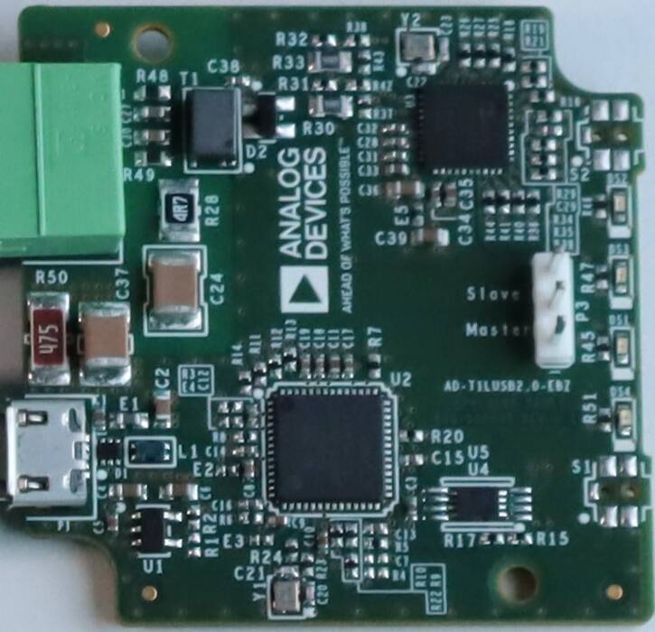
The AD-SWIOT1L-SL kit includes a 10BASE-T1L to USB adapter AD-T1LUSB2.0-EBZ which is useful to directly control the board via a USB connection.
Note
Check out here the User Guide for AD-T1LUSB2.0-EBZ
Besides this, other 10BASE-T1L media converters like the EVAL-ADIN1100 can be used to directly interface the AD-SWIOT1L-SL board on an Ethernet network.
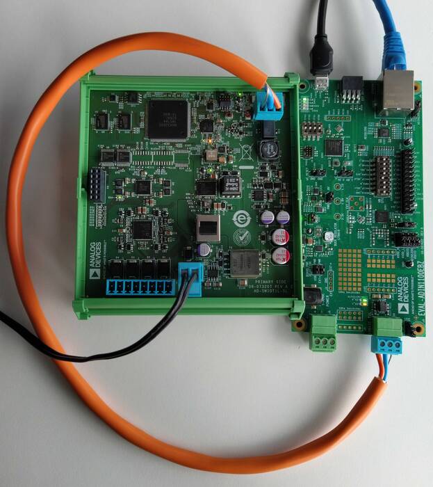
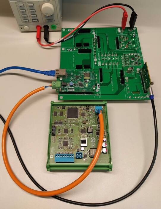
Figure 17 AD-SWIOT1L-SL with EVAL-ADIN1100 10BASE-T1L Media Converter
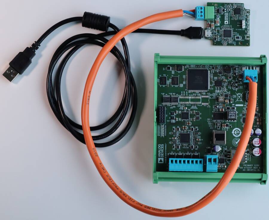
Figure 18 AD-SWIOT1L-SL with AD-T1LUSB-EBZ 10BASE-T1L to USB Adapter
Single-pair Power over Ethernet (SPoE)
As mentioned earlier, in the introduction section, the AD-SWIOT1L-SL board can be powered via the SPoE technology. For this, we mainly need to use the LTC9111 Powered Device (PD) controller, included on the board, and the companion part LTC4296-1 five port, Single-pair Power over Ethernet (SPoE), Power Sourcing Equipment (PSE) controller.
The purpose of the LTC9111 PD controller is to communicate the power classification and to provide protection against undervoltage or overvoltage scenarios. In contrast, the LTC4296-1 PSE controller will initiate the communication for power classification and it will provide protection against overcurrents and other energy surges events.
The communication between PD classification is made via the Serial Communication Classification Protocol (SCCP) and is initiated before the power over data lines is turned on.
On the AD-SWIOT1L-SL board, the LTC9111 circuitry is configurated to function as a class 12 PD device, which means that it will only function together with a PSE equipment configurated only in class 12.
LED Indicators
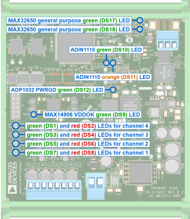
There are a couple of LEDs present on the board which are used to indicate particular system statuses.
To easily identify if the system is powered properly, there is a green LED around the ADP1032 power supply which will indicate if the 24 V and 3.3 V rails for the software configurable I/0 devices are within margins, by being lit and another green LED which will be also lit if the 24 V supply for MAX14906 is present.
Around the ADIN1110 there are also two LEDs, green and yellow, which depending on the software configuration, can be used to indicate different network statuses.
The MAX14906 has also a LED matrix, with red and green LEDs, that can be used to eider indicate the channels’ statuses and faults or can be used as general-purpose indicators.
Finally, there are also two green LEDs around the P1 programming connector (SWD) which can be controlled directly by the MAX32650 microcontroller (MCU).
Thermal Info
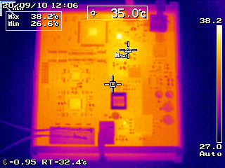
The operating temperature of the AD-SWIOT1L-SL board before it is configured will be around 10°C over the ambient temperature.
The maximum temperature of the AD74413R circuitry when is operating at maximum power.
This is the situation when all channels are using the AD74413R sourcing functions at the maximum limit, for example, all channels are sourcing 25 mA.
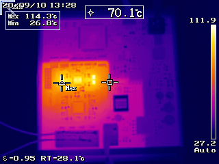
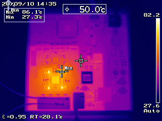
The maximum temperature of the MAX14906 circuitry when is operating at maximum power.
This is the situation when all channels are using the MAX14906 digital output functions with the current limit set at maximum and a load that is draining almost the maximum available power, for example, from all channels the load is draining 1.2 A.
This is usually the worst-case scenario when the AD-SWIOT1L-SL board will heat up at the highest temperature.
Support
Analog Devices will provide limited online support for anyone using the reference design with Analog Devices components via the EngineerZone Reference Designs forum.