AD9371 Advanced
General Description
The AD9371 Advanced plugin provides low-level configuration of the AD9371 transceiver. Settings
map directly to the mykonosDevice_t structure used by the No-OS driver and to devicetree
properties used by the Linux driver.
Most settings are written to internal buffers when changed. To apply the settings to hardware and trigger device reinitialization and calibration, press Save Settings. The exception is the BIST tab, where all controls take effect immediately without requiring Save Settings.
The Advanced tool is organized into 13 tabs displayed in two navigation rows at the top of the panel.
Clock Settings
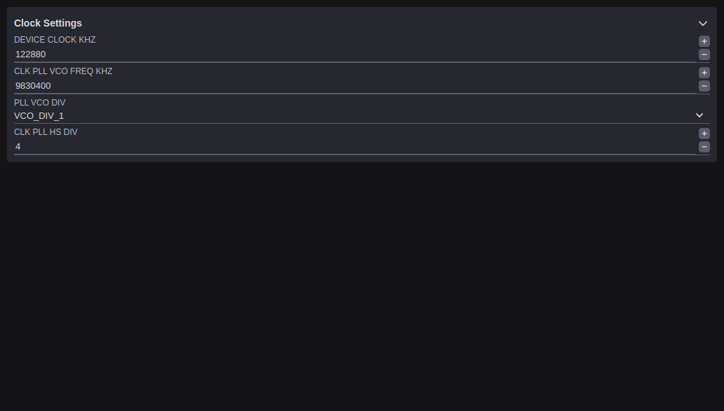
Configures the device PLL and clock generation parameters.
High-Speed Divider: Sets the high-speed clock divider ratio.
VCO Divider: Sets the VCO output divider ratio.
VCO Frequency (kHz): Displays or sets the VCO operating frequency in kHz.
Device Clock Frequency (kHz): Sets the reference device clock frequency in kHz.
Calibrations
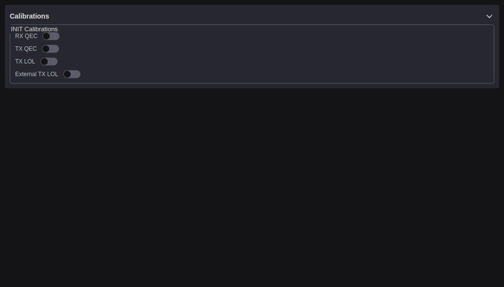
Selects which calibrations are run during device initialization. Each calibration can be enabled or disabled independently via a bitmask.
TX BB Filter: Calibrates the transmit baseband filter.
ADC Tuner: Calibrates the ADC tuning for optimal performance.
TIA 3dB Corner: Sets the transimpedance amplifier bandwidth corner.
DC Offset: Calibrates DC offset in the signal path.
TX Attenuation Delay: Compensates for attenuation delay in the TX path.
RX Gain Delay: Compensates for gain delay in the RX path.
Flash Cal: Performs flash-based calibration.
Path Delay: Calibrates the signal path delay for DPD purposes.
TX LO Leakage Internal: Runs TX LO leakage calibration using the internal loopback path.
TX LO Leakage External: Runs TX LO leakage calibration using the external ORx path.
TX QEC: Runs transmit quadrature error correction calibration.
RX LO Delay: Calibrates receive LO delay.
RX QEC Init: Runs the initial receive quadrature error correction calibration.
CLGC: Runs the Closed-Loop Gain Control calibration (AD9375 only).
VSWR: Runs the VSWR detection calibration (AD9375 only).
TX Settings
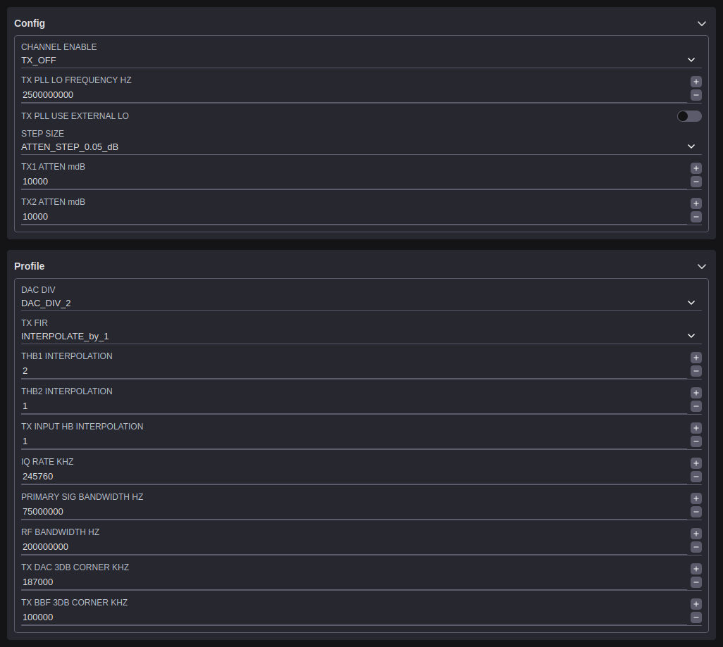
Configures the transmit channel data path and profile parameters.
TX Channels: Selects which TX channels are enabled (TX1, TX2, or both).
TX PLL Use External LO: When enabled, uses an external LO reference instead of the internal PLL.
TX Profile: Displays the active TX profile bandwidth and sample rate configuration.
Primary Signal Bandwidth (Hz): The primary signal bandwidth of the TX channel.
TX Input Rate (kSPS): The input sample rate at the TX digital interface in kSPS.
TX Interpolation: The overall interpolation factor applied in the TX data path.
FIR Decimation: The decimation factor applied in the TX FIR filter stage.
IQ Rate (kSPS): The TX I/Q sample rate at the DAC input in kSPS.
RF Bandwidth (Hz): The RF bandwidth of the TX channel.
ADC Clock Rate (kHz): The clock rate supplied to the TX auxiliary ADC.
FIR Filter: Displays the active TX FIR filter coefficient set.
RX Settings
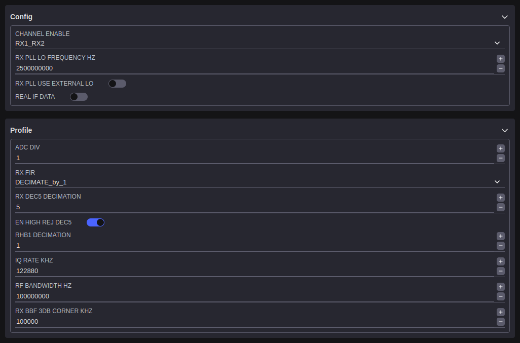
Configures the receive channel data path and profile parameters.
RX Channels: Selects which RX channels are enabled (RX1, RX2, or both).
RX PLL Use External LO: When enabled, uses an external LO reference instead of the internal PLL.
RX Profile: Displays the active RX profile bandwidth and sample rate configuration.
Primary Signal Bandwidth (Hz): The primary signal bandwidth of the RX channel.
RX Output Rate (kSPS): The output sample rate at the RX digital interface in kSPS.
RX Decimation: The overall decimation factor applied in the RX data path.
FIR Decimation: The decimation factor applied in the RX FIR filter stage.
IQ Rate (kSPS): The RX I/Q sample rate at the ADC output in kSPS.
RF Bandwidth (Hz): The RF bandwidth of the RX channel.
ADC Clock Rate (kHz): The clock rate supplied to the RX ADC.
FIR Filter: Displays the active RX FIR filter coefficient set.
Observation RX Settings
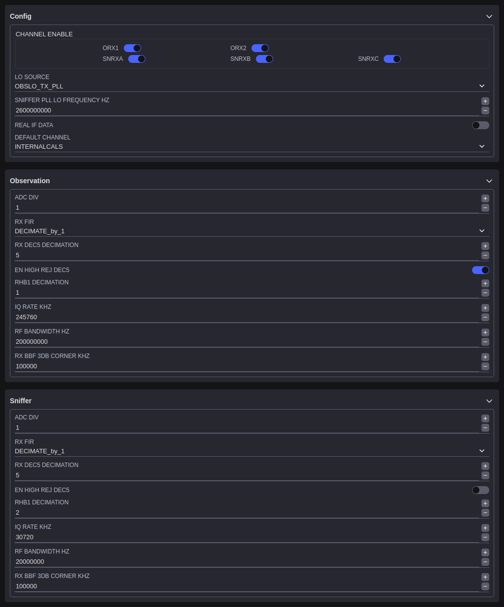
Configures the observation receiver (ORx) data path, which is used for TX calibration monitoring.
ORx Channels: Selects which observation receiver channels are enabled.
ORx Output Rate (kSPS): The output sample rate of the observation receiver.
ORx RF Bandwidth (Hz): The RF bandwidth of the observation receiver.
ORx ADC Clock Rate (kHz): The ADC clock rate for the observation receiver.
Sniffer RF Bandwidth (Hz): The RF bandwidth of the sniffer port.
Sniffer Output Rate (kSPS): The output sample rate of the sniffer port.
Gain Setup
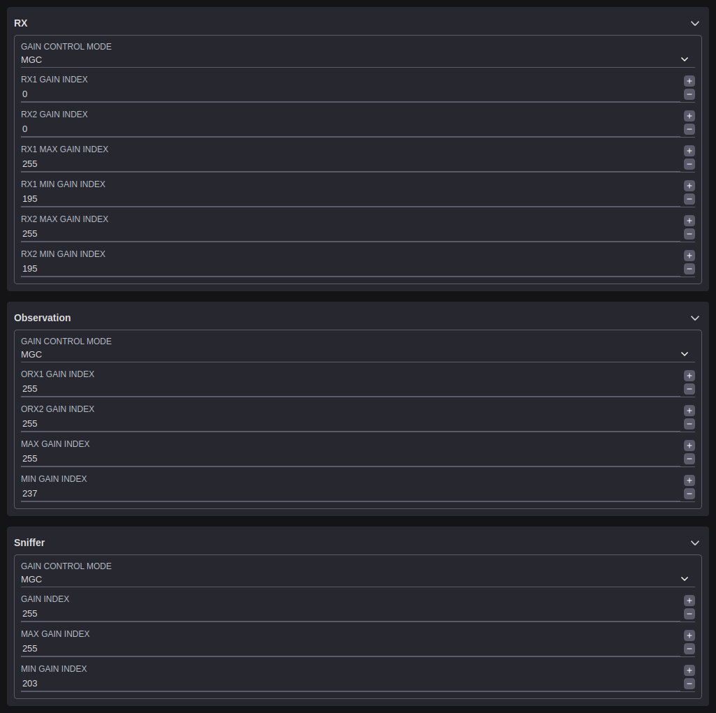
Configures manual gain control parameters for the receive path.
RX1 Manual Gain Index: Sets the gain table index for RX channel 1 when in MGC mode.
RX2 Manual Gain Index: Sets the gain table index for RX channel 2 when in MGC mode.
ORx Manual Gain Index: Sets the gain table index for the observation receiver in MGC mode.
Sniffer Manual Gain Index: Sets the gain table index for the sniffer port in MGC mode.
AGC Setup
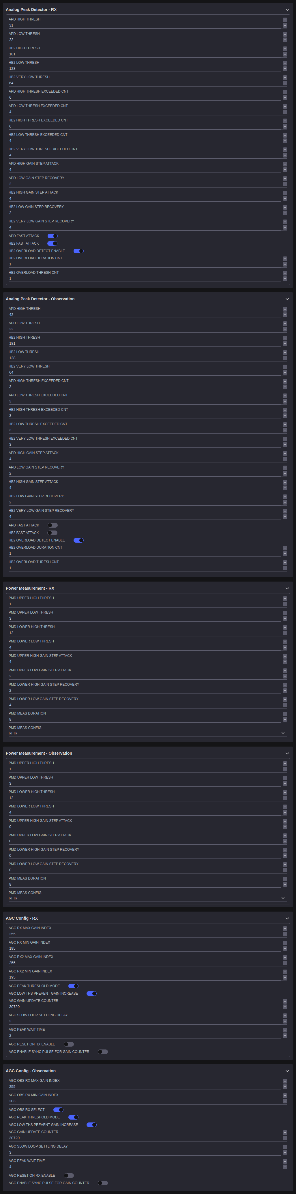
Configures the Automatic Gain Control (AGC) for the receive path.
Peak Wait Time: The number of samples the AGC waits after a gain change before checking for a peak.
Gain Update Time (us): The interval in microseconds at which the AGC updates the gain index.
Low Threshold Prevent Gain Inc: Prevents gain increases when the signal is near the low power threshold.
Gain Change If Threshold High: Enables a gain change when the signal exceeds the high power threshold.
AGC Slow Loop Settling Delay: The number of samples the slow loop waits after settling before updating the gain.
ADC High Ovrg Exceed Threshold: The number of ADC overrange events that must occur to trigger a gain decrease.
ADC Peak Threshold: Sets the ADC input level (dBFS) that triggers a peak detection event.
Under Range High Threshold: The lower signal level boundary for the high range band.
Under Range Low Threshold: The lower signal level boundary for the low range band.
Over Range High Threshold: The upper signal level boundary for the high range band.
Over Range Low Threshold: The upper signal level boundary for the low range band.
ARM GPIO
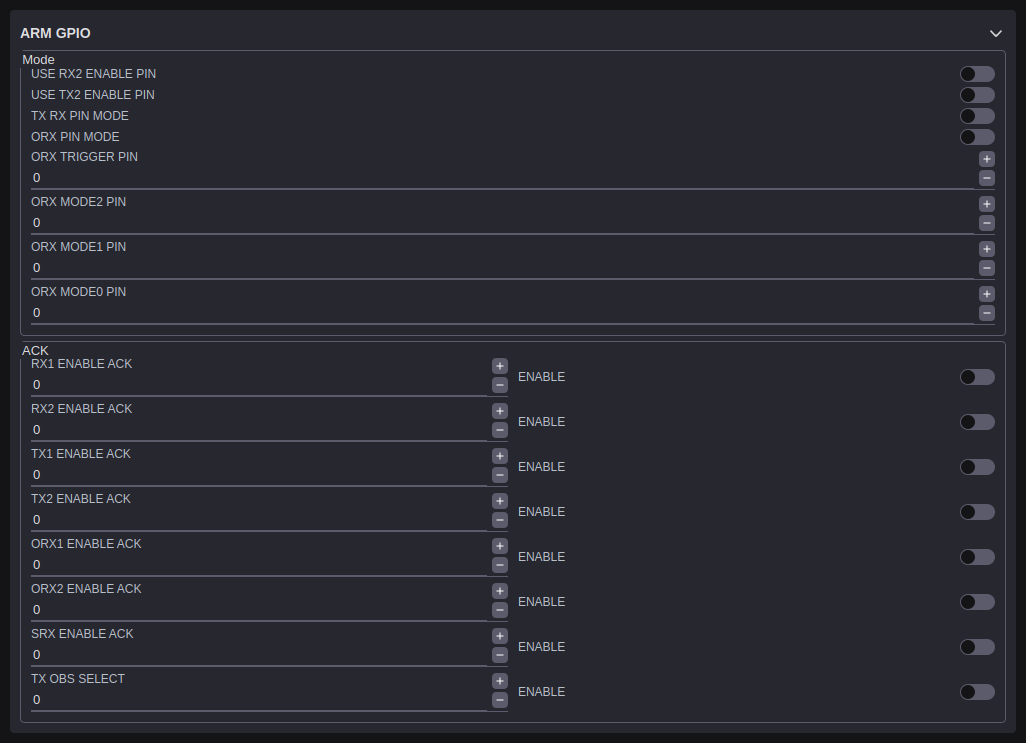
Configures the GPIO pins controlled by the device ARM processor.
TX RX Select Pin: Selects the GPIO pin used to switch between TX and RX modes.
RX2 Enable Pin: Selects the GPIO pin used to enable the second RX channel.
Enable Pin: Selects the GPIO pin that acts as the global enable signal.
ORXEN A/B Pin: Selects the GPIO pins used to enable the observation receiver.
GPIO
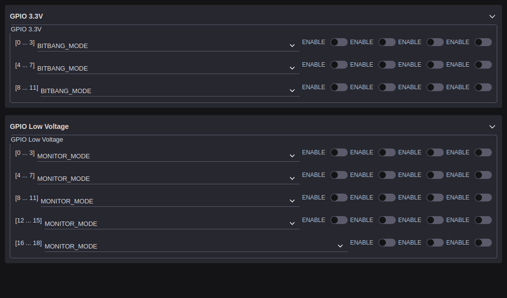
Configures the general-purpose GPIO pins for monitoring and control functions.
GPIO Source Control: Sets the source control register for each GPIO pin, selecting whether the pin is driven by the ARM, BBIC, or a specific analog signal.
3.3V GPIO Output Enable Mask: A bitmask enabling the 3.3V GPIO output drivers. Each bit corresponds to one 3.3V GPIO pin.
AUX DAC
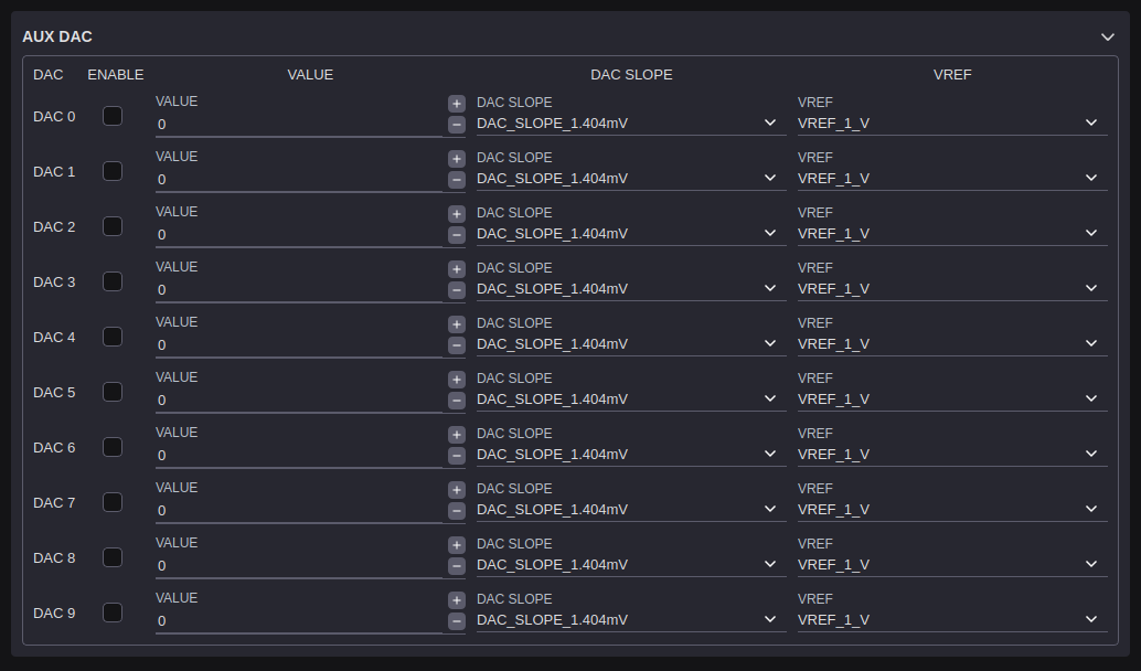
Configures the auxiliary DAC outputs for analog signal generation.
AUX DAC Enable Mask: A bitmask selecting which AUX DAC outputs are enabled.
AUX DAC Word (0–4095): Sets the 12-bit digital code for each enabled AUX DAC output, where 0 corresponds to 0 V and 4095 to the full-scale voltage.
AUX DAC Slope: Configures the gain slope applied to the AUX DAC output.
AUX DAC VBias: Sets the bias voltage for the AUX DAC output stage.
JESD Framer
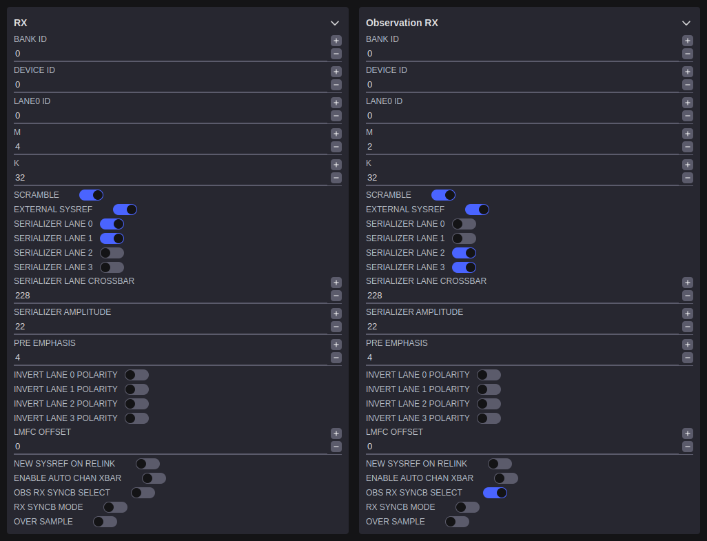
Configures the JESD204B framer used for the RX and ORx data paths.
Bank ID: Sets the JESD204B bank ID (0–15).
Device ID: Sets the JESD204B device ID.
Lane 0 ID: Sets the lane identification number for lane 0.
M: Number of converters per device.
K: Number of frames per multiframe.
F: Number of octets per frame.
NP: Total number of bits per sample.
Scramble: Enables or disables JESD204B data scrambling.
External SYSREF: Selects an external SYSREF source.
Serializer Lanes Enabled: Bitmask of enabled serializer lanes.
Serializer Lane Crossbar: Maps logical lanes to physical serializer lanes.
Oversampling: Sets the oversampling ratio.
JESD Deframer
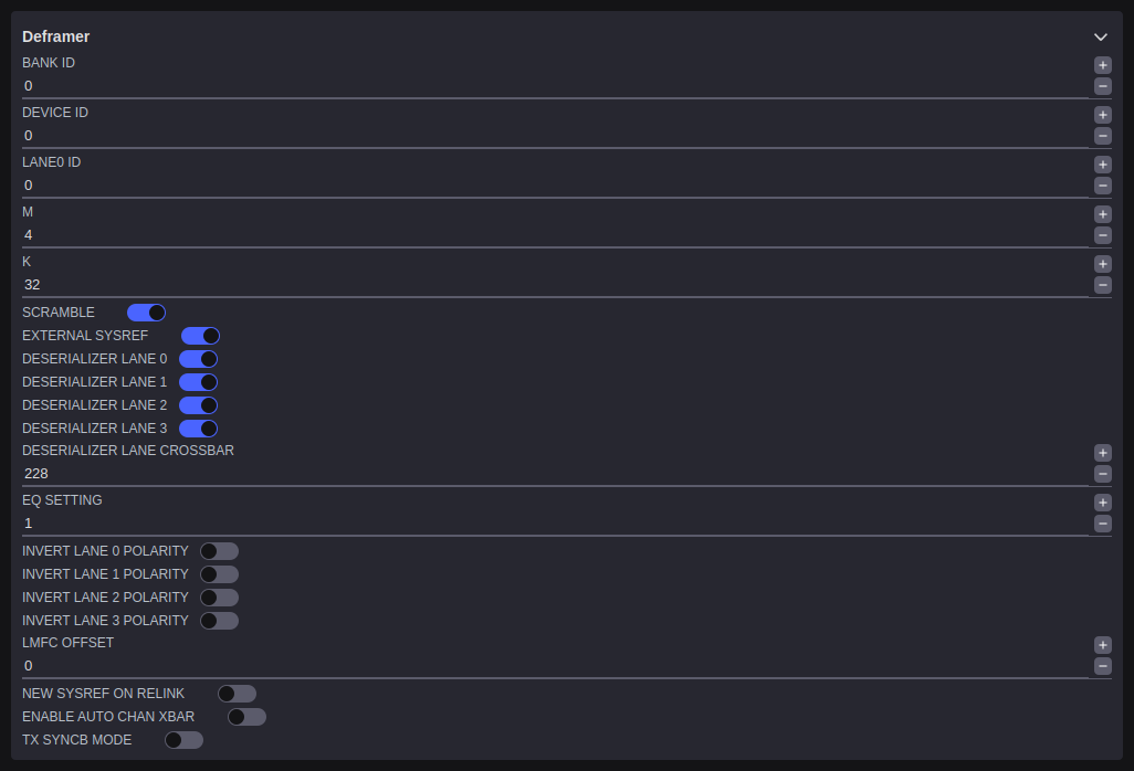
Configures the JESD204B deframer used for the TX data path.
Bank ID: Sets the JESD204B bank ID (0–15).
Device ID: Sets the JESD204B device ID.
Lane 0 ID: Sets the lane identification number for lane 0.
M: Number of converters per device.
K: Number of frames per multiframe.
Scramble: Enables or disables JESD204B data scrambling.
External SYSREF: Selects an external SYSREF source.
Deserializer Lanes Enabled: Bitmask of enabled deserializer lanes.
Deserializer Lane Crossbar: Maps logical lanes to physical deserializer lanes.
BIST
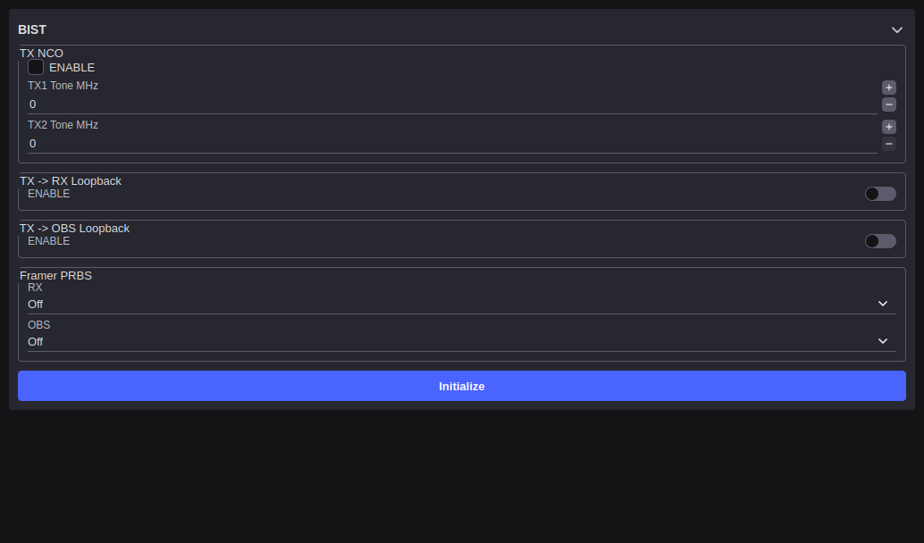
Built-In Self-Test (BIST) provides diagnostic signal paths for verifying the device data path. All BIST controls take effect immediately without requiring the Save Settings button.
Tone Injection Frequency (kHz): Injects a test tone at the specified frequency in kHz into the receive data path for signal integrity testing.
PRBS Type (RX): Selects the Pseudorandom Binary Sequence pattern injected into the receive path for bit error rate testing.
PRBS Type (TX): Selects the PRBS pattern injected into the transmit path.
Loopback Mode: Enables a digital loopback path from the TX data path back into the RX data path, allowing end-to-end digital path verification without an RF signal.