ADRV9009 Advanced
Description
The ADRV9009 Advanced plugin provides direct access to low-level device attributes and specialized configuration options that are not available in the basic ADRV9009 plugin. This tool exposes the underlying ADRV9009 device attributes through organized collapsible sections, allowing expert users to configure advanced device parameters directly.
The advanced plugin is organized into up to 15 navigation tabs (depending on implementation branch) with expandable/collapsible interface that adapts to window width:
- Implemented Sections:
CLK Settings - Device clock and PLL configuration
Calibrations - Calibration mask configuration and controls
TX Settings - Advanced transmitter configuration
RX Settings - Advanced receiver configuration
ORX Settings - Observation receiver configuration
FHM Setup - Frequency hopping mode configuration
PA Protection - Power amplifier protection settings
GAIN Setup - Gain control and AGC configuration
AGC Setup - Automatic gain control algorithm settings
GPIO Config - General purpose I/O configuration
AUX DAC - Auxiliary DAC controls for 12 independent channels
JESD204 Settings - JESD204 interface configuration
JESD Framer - JESD204 framer configuration (JESD branch only)
JESD Deframer - JESD204 deframer configuration (JESD branch only)
BIST - Built-in self-test features
Warning: The advanced plugin exposes low-level device attributes. Improper configuration may result in device malfunction or sub-optimal performance. Ensure you have adequate knowledge of ADRV9009 operation before using these features.
CLK Settings
The CLK Settings section provides direct control over ADRV9009 clock and PLL configuration through 5 specific device attributes:
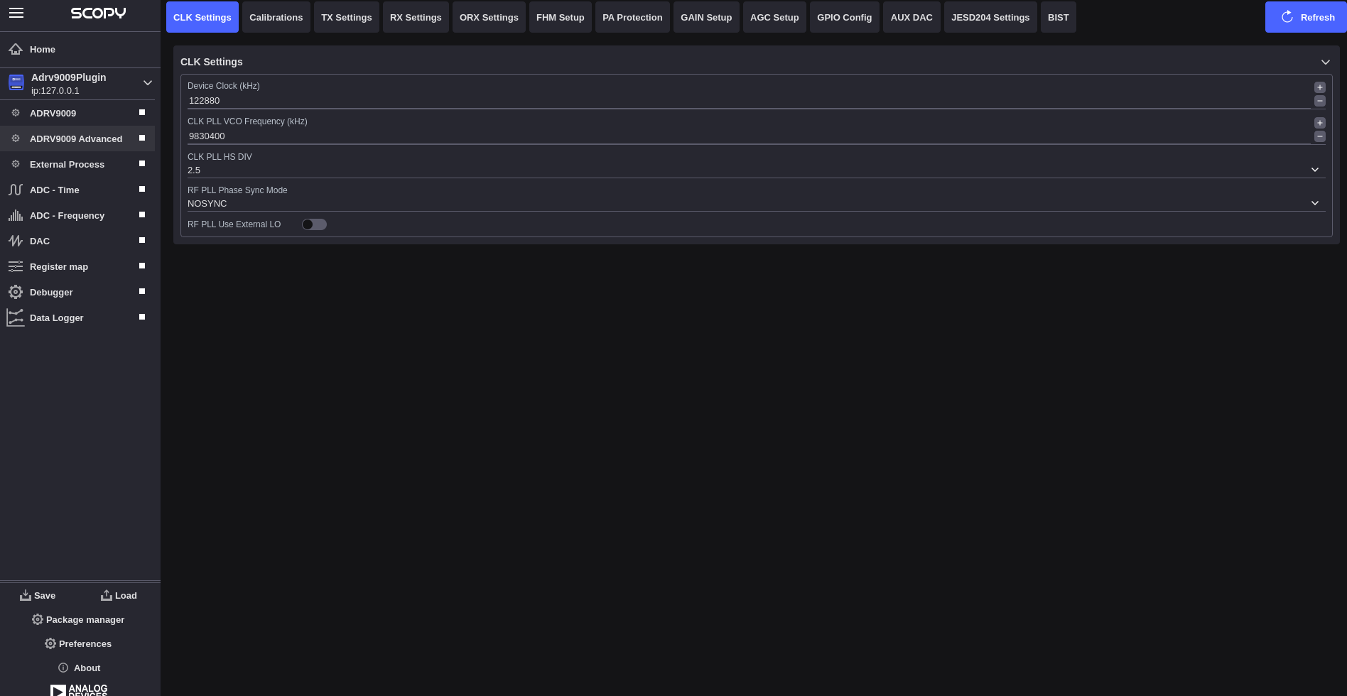
- Device Clock (kHz):
Range: [10000 - 1000000] kHz in 1 kHz steps
Description: Main device clock frequency configuration
- CLK PLL VCO Frequency (kHz):
Range: [6000000 - 12000000] kHz in 1 kHz steps
Description: Clock PLL VCO frequency setting
- CLK PLL HS DIV:
Options: 2, 2.5, 3, 4, 5 (mapped from device values 0,1,2,3,4)
Description: Clock PLL high-speed divider selection
- RF PLL Phase Sync Mode:
Options: NOSYNC, INIT_TRACK, INIT_1TRACK, INIT_CONTTRACK (mapped from device values 0,1,2,3)
Description: RF PLL phase synchronization mode selection
- RF PLL Use External LO:
Description: Enable external local oscillator for RF PLL
Calibrations
The Calibrations section provides control over the ADRV9009 calibration mask through 6 calibration type checkboxes. Changes to any calibration checkbox immediately write the calibration mask to the device.
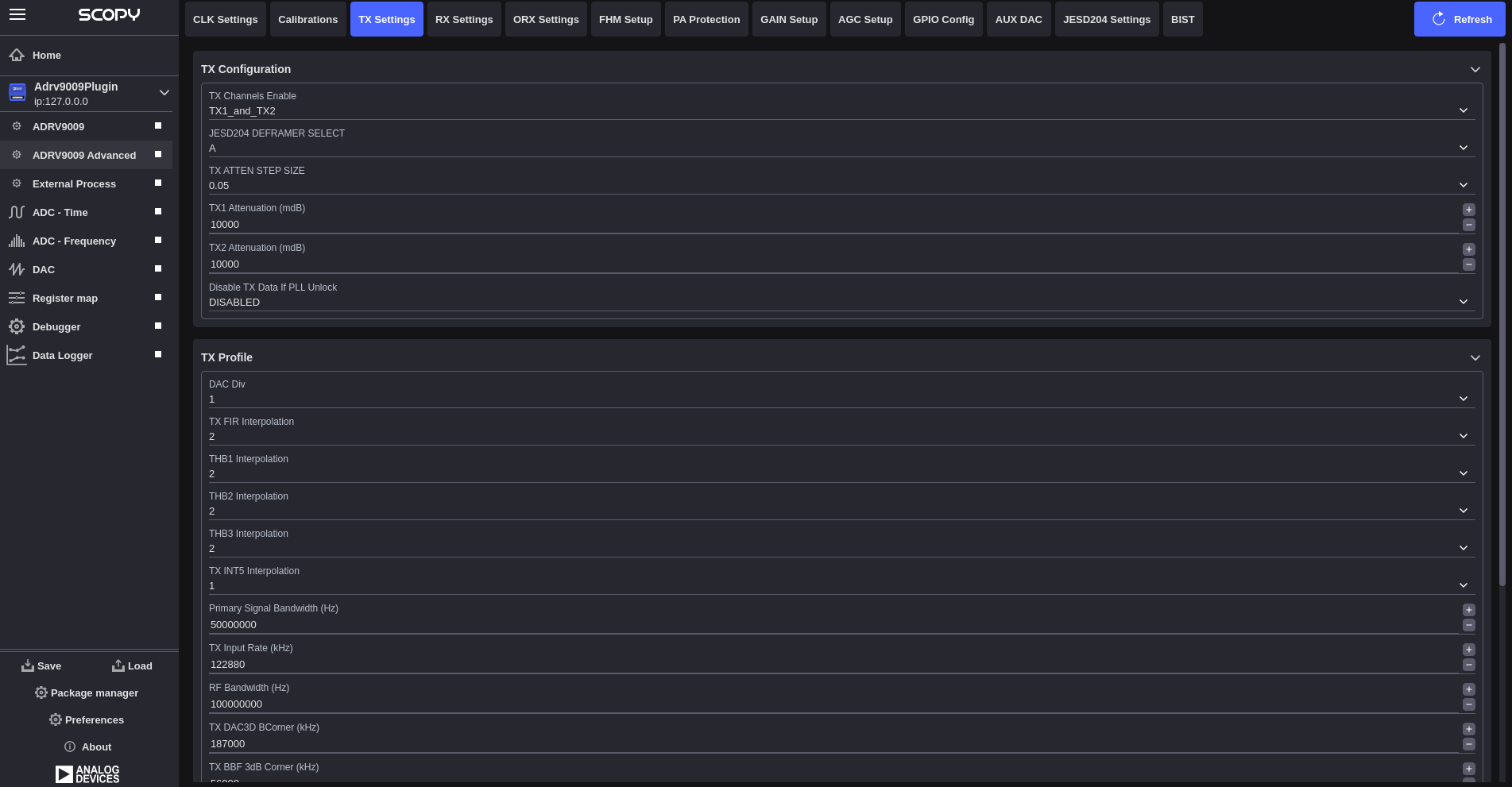
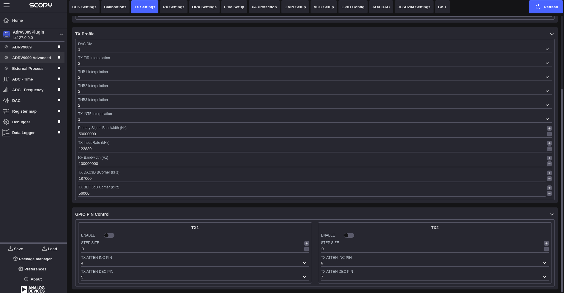
TX Settings
The TX Settings section provides advanced transmitter configuration through 16 attributes organized in 3 collapsible sections:
TX Configuration Section: Low-level transmitter profile and sampling configuration controls.
- TX Profile Section (9 attributes):
DAC Div: DAC divider selection
TX FIR Interpolation: FIR filter interpolation factor
RHBD Decimation: RHBD decimation factor
THB1 Interpolation: THB1 interpolation factor
THB2 Interpolation: THB2 interpolation factor
THB3 Interpolation: THB3 interpolation factor
TX BBF 3dB Corner (kHz): Range [20000-250000] kHz - baseband filter corner frequency
TX DAC 3dB Corner (kHz): Range [50000-750000] kHz - DAC filter corner frequency
TX BBF 3dB Corner Table: Range [0-15] - filter corner frequency table index
TX GPIO PIN Control Section: GPIO pin configuration for transmitter-related control signals and interfaces.
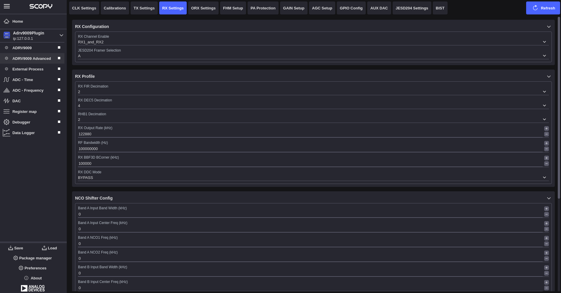
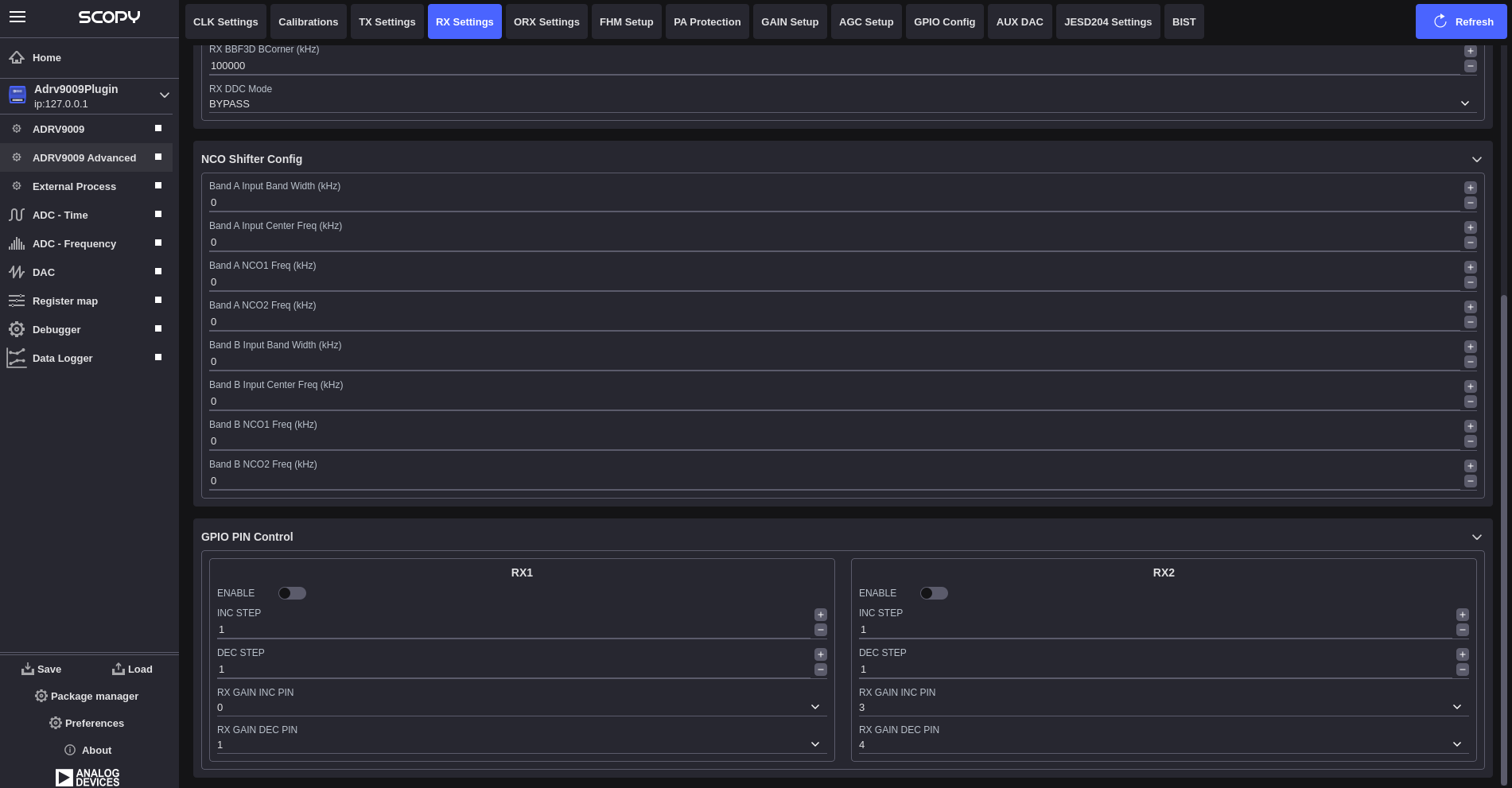
RX Settings
The RX Settings section provides advanced receiver configuration through 25 attributes organized in 4 collapsible sections:
RX Configuration Section: Low-level receiver profile and sampling configuration controls.
- RX Profile Section (7 attributes):
RX FIR Decimation: FIR filter decimation factor
RX Dec5 Decimation: Dec5 decimation factor
RHBD Decimation: RHBD decimation factor
RX ADC Profile: ADC profile selection
RX DDC Mode: DDC mode configuration
RX BBF 3dB Corner (kHz): Range [20000-250000] kHz - baseband filter corner frequency
RX ADC 3dB Corner (kHz): Range [50000-750000] kHz - ADC filter corner frequency
NCO Shifter Config Section: Numerically controlled oscillator configuration for frequency shifting applications.
RX GPIO PIN Control Section: GPIO pin configuration for receiver-related control signals and interfaces.
ORX Settings
The ORX (Observation RX) Settings section provides advanced observation receiver configuration through multiple collapsible sections:
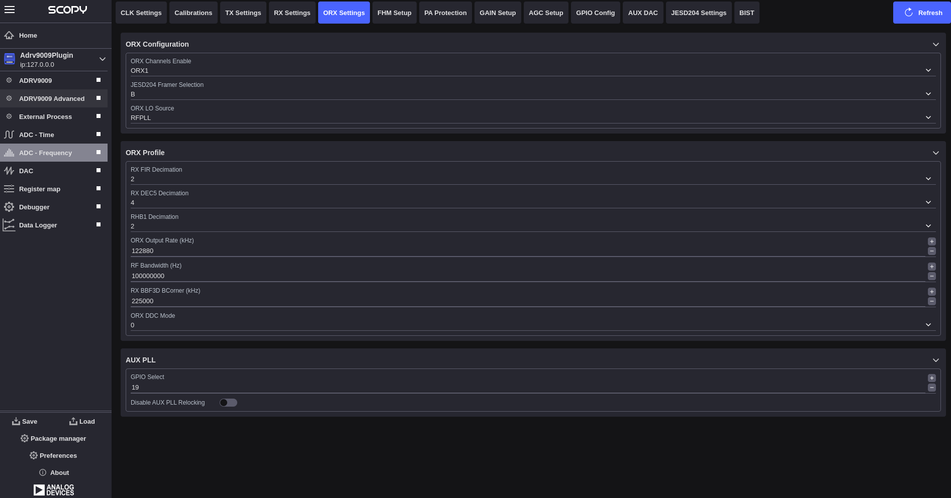
ORX Configuration Section: Low-level observation receiver profile and sampling configuration controls.
ORX Profile Section: Observation receiver filter and sampling rate configuration parameters.
ORX GPIO PIN Control Section: GPIO pin configuration for observation receiver control signals and interfaces.
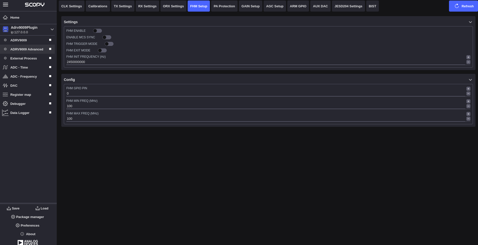
FHM Setup
The FHM (Frequency Hopping Mode) Setup section provides frequency hopping configuration controls.
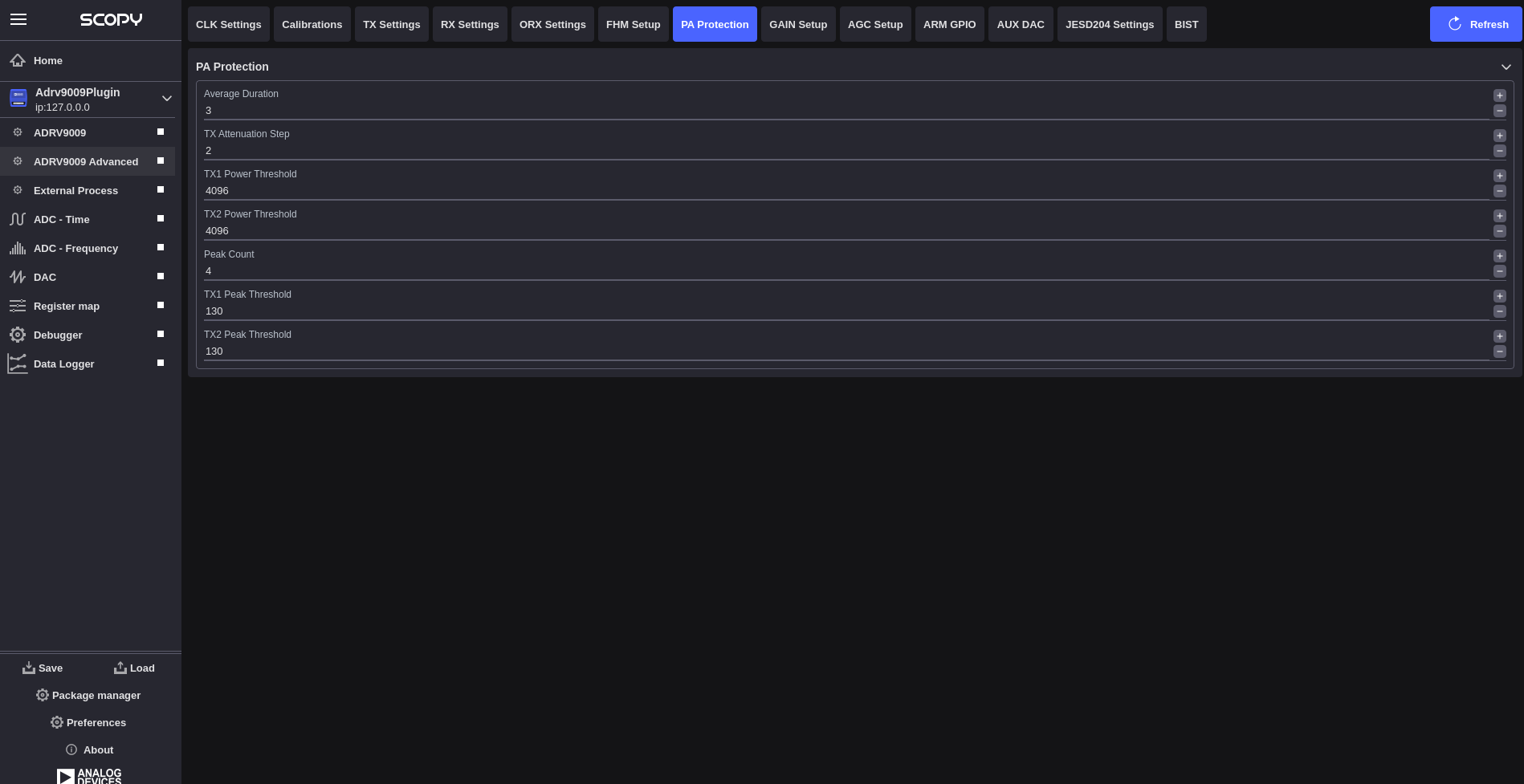
PA Protection
The PA (Power Amplifier) Protection section provides power amplifier protection configuration controls.
GAIN Setup
The GAIN Setup section provides gain control configuration through 14 attributes organized in 2 collapsible sections:
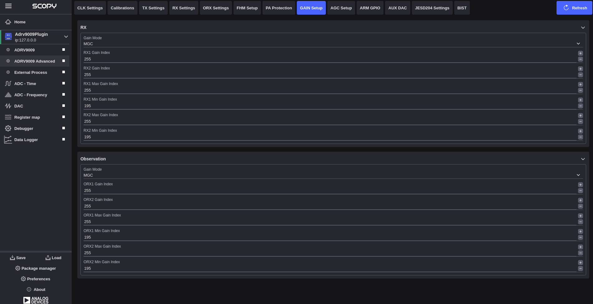
- RX Section (7 attributes):
Gain Mode: gain control mode selection
Peak AGC Upper Threshold: Range [0-31] - upper AGC threshold setting
Peak AGC Lower Threshold: Range [0-31] - lower AGC threshold setting
Peak AGC Gain Step: Range [0-31] - AGC gain step size
Peak AGC Attack Delay: Range [0-63] - AGC attack delay setting
Peak AGC Recovery Delay: Range [0-2047] - AGC recovery delay setting
Low Power Threshold: Range [0-15] - low power detection threshold
Observation Gain Section (7 attributes): Similar gain control parameters specifically for the observation receiver path.
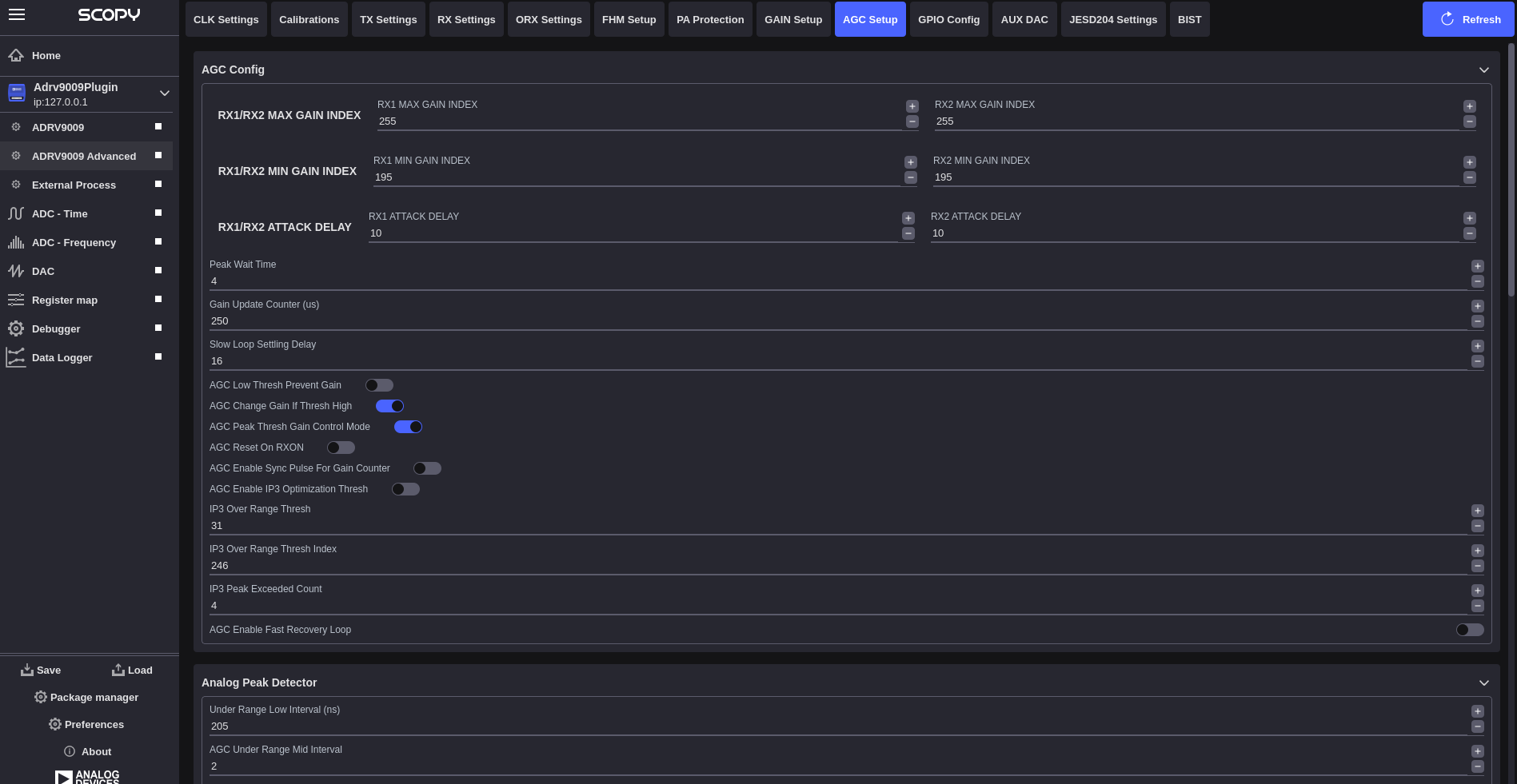
AGC Setup
The AGC Setup section provides automatic gain control algorithm configuration:
AGC Configuration: Primary AGC algorithm configuration parameters and mode selection.
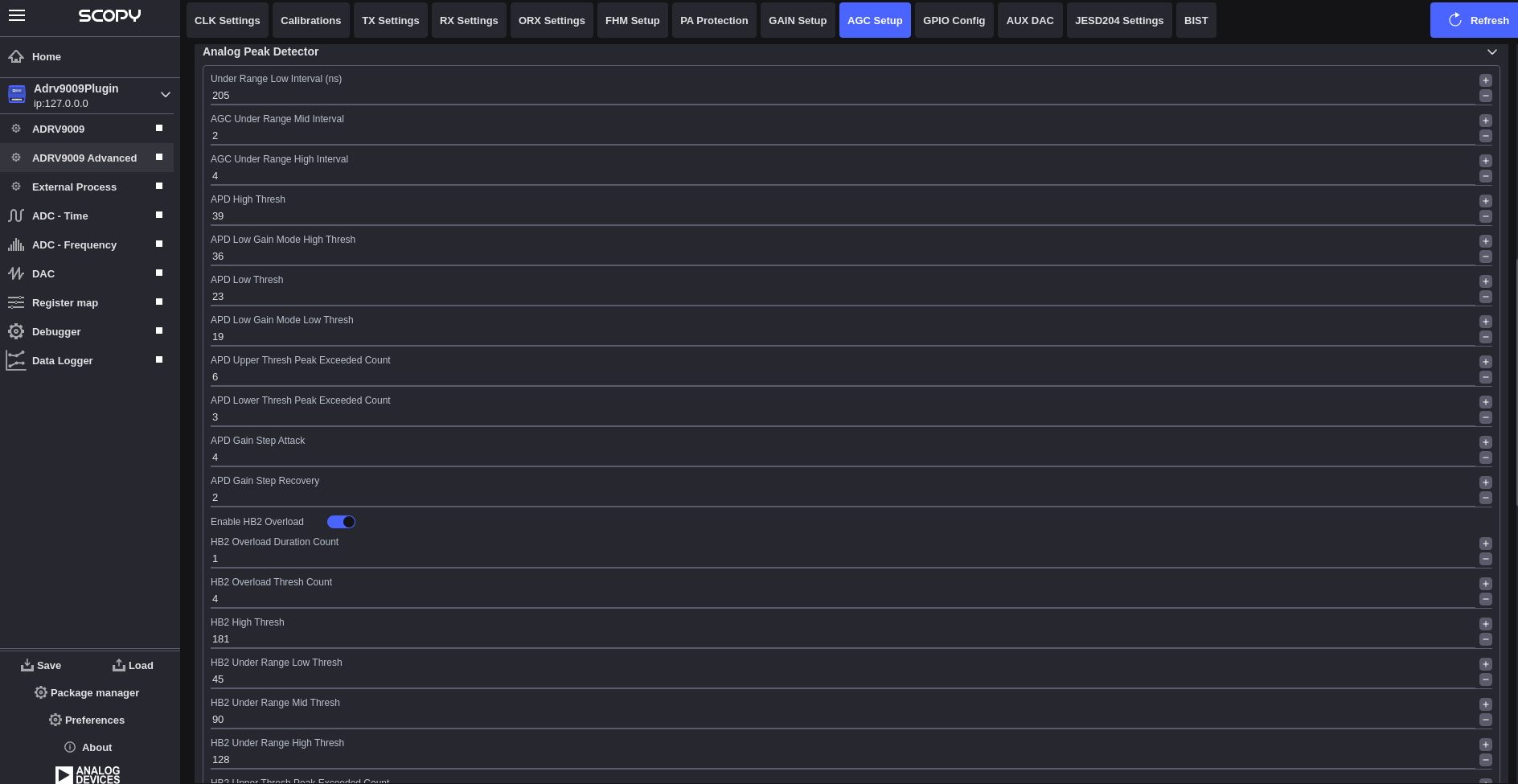
Analog Peak Detector: Peak detection based AGC configuration and threshold settings.
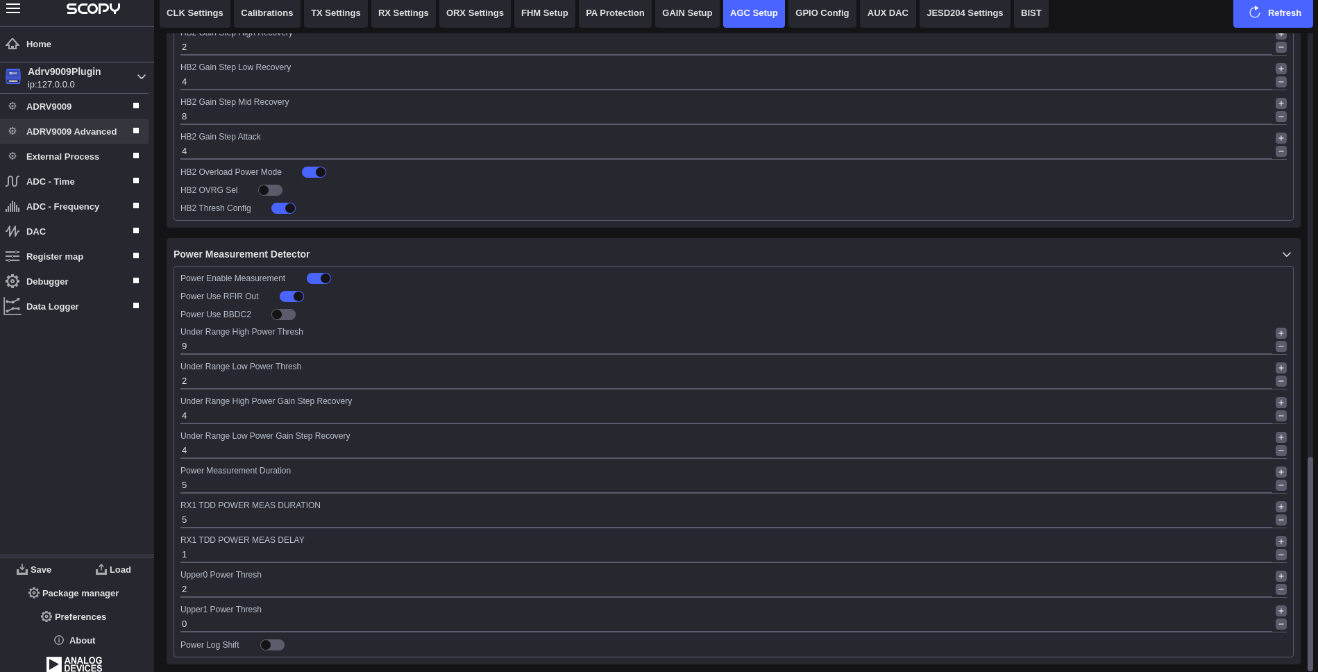
Power Measurement Detector: Power measurement based AGC configuration and performance parameters.
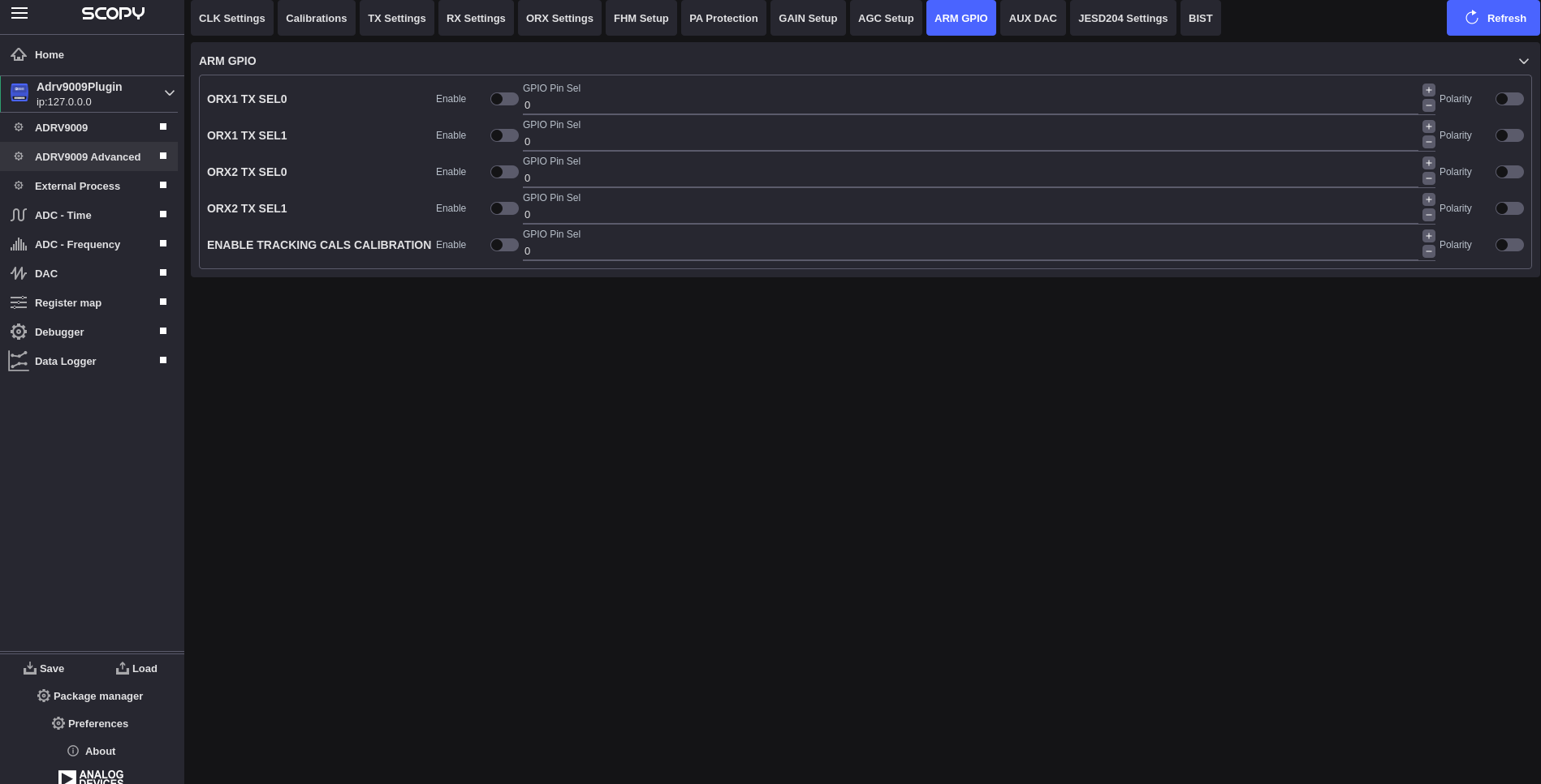
GPIO Config
The GPIO Config section provides ARM GPIO configuration implemented as part of the gain_fhm_pa_gpio branch.
AUX DAC
The AUX DAC section provides auxiliary digital-to-analog converter configuration for 12 independent DAC channels through a tabular interface:
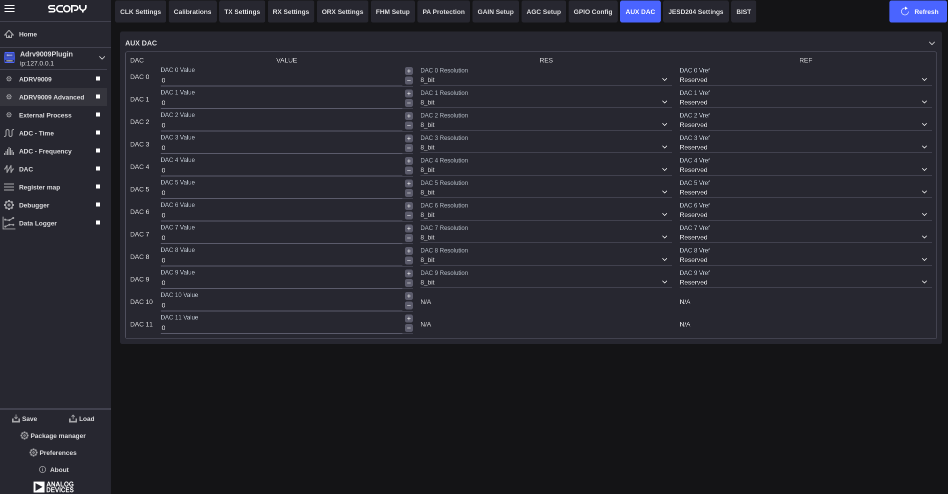
DAC Channel Configuration:
- Standard Channels (DAC 0-9):
DAC Value: Numeric output value setting for the DAC channel
Resolution: Configurable DAC resolution
Voltage Reference: Selectable voltage reference for the DAC output
- Limited Channels (DAC 10-11):
DAC Value: Numeric output value setting
Resolution: N/A (not configurable)
Voltage Reference: N/A (not configurable)
The interface provides direct control over ADRV9009’s auxiliary DAC outputs for applications requiring analog control signals or reference voltages.
JESD204 Settings
The JESD204 Settings section provides JESD204 interface configuration through 13 attributes in a single collapsible section:
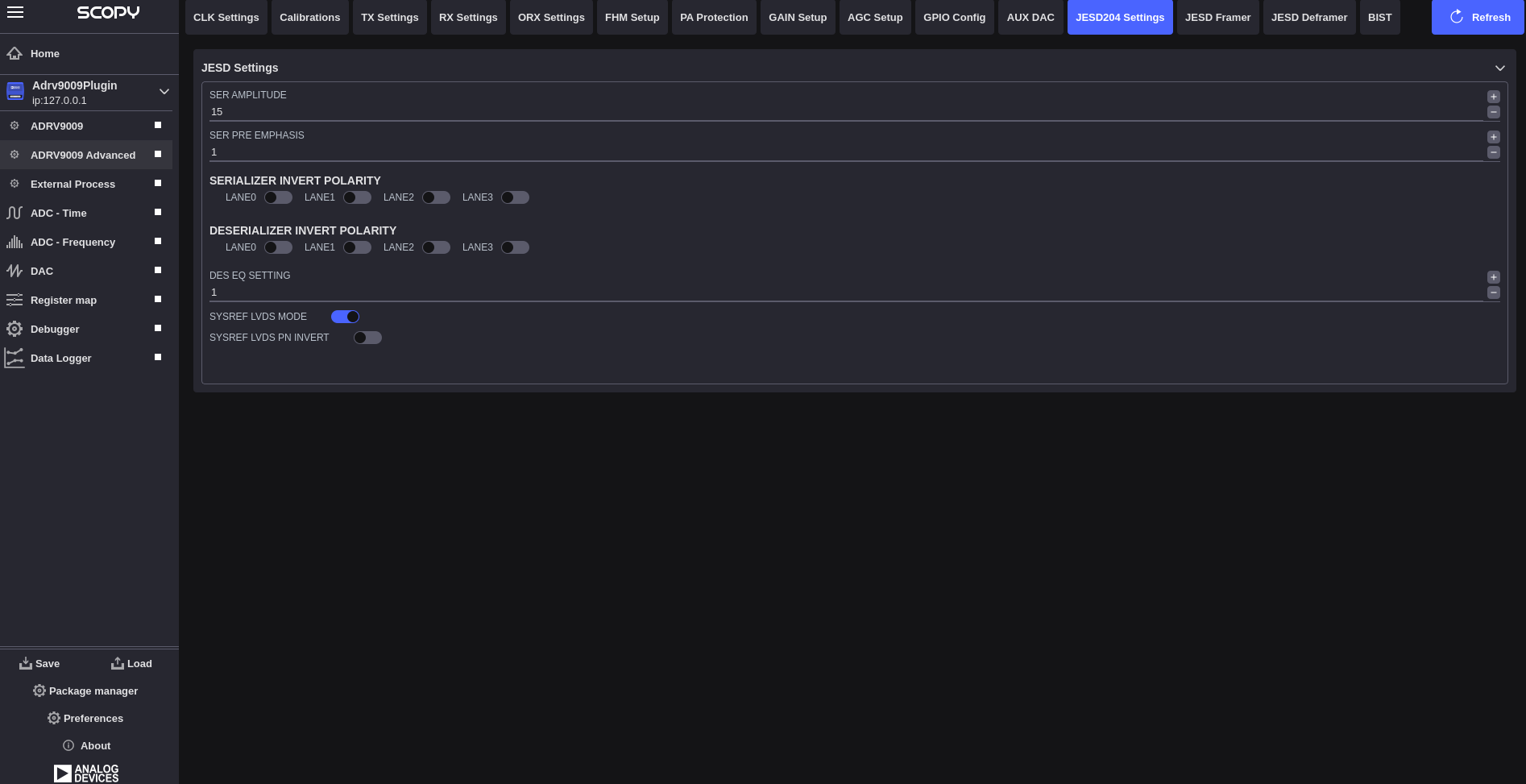
- JESD Settings Section:
Device JESD204 Link0 Converter Select: Combobox for converter selection
Device JESD204 Link0 JESD Mode: Combobox for JESD mode configuration
Device JESD204 Link0 Subclass: Combobox for subclass selection
Device JESD204 Link0 DualLink: Combobox for dual link configuration
Device JESD204 Link0 Version: Combobox for JESD204 version selection
Additional link configuration parameters and settings (8 more attributes)
JESD Framer
Available in JESD branch only
The JESD Framer section provides dedicated JESD204 framer configuration through 39 attributes organized in A|B column layout:
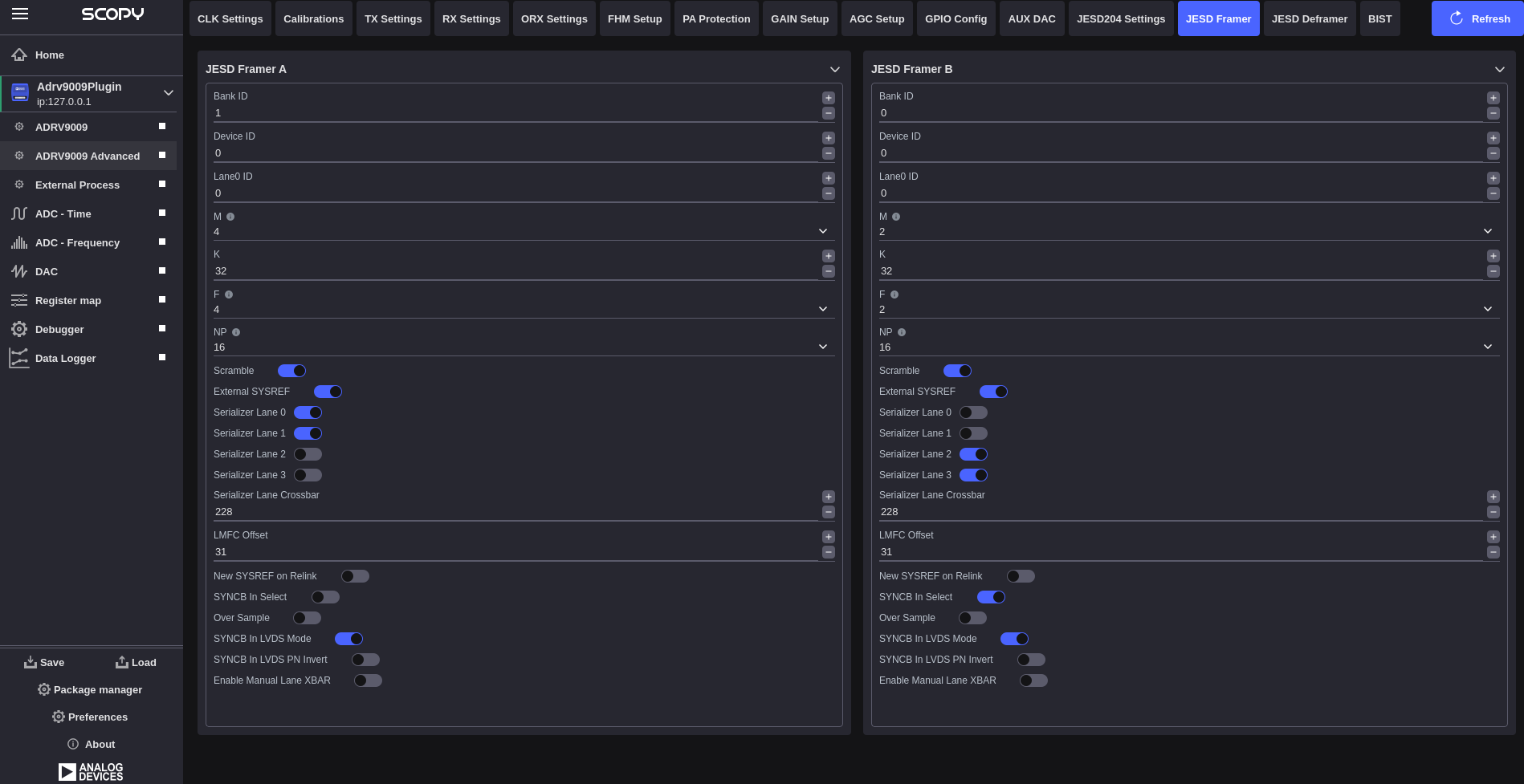
- JESD Framer A (22 attributes):
Bank ID: Range [0-15]
Device ID: Range [0-255]
Lane0 ID: Range [0-31]
M: Number of ADCs [0,2,4]
K: Frames per multiframe [1-32]
F: Bytes per frame [1,2,3,4,6,8]
NP: Sample resolution [12,16,24]
Scramble: Enable/disable scrambling
External SYSREF: System reference control
Serializer Lane 0-3: Individual lane controls
Serializer Lane Crossbar: Range [0-65535]
LMFC Offset: Range [0-31]
New SYSREF on Relink: Relink control
SYNCB In Select: SYNCB input selection
Over Sample: Over sampling control
Additional SYNCB and configuration controls
- JESD Framer B (17 attributes):
Similar framer configuration for second framer path
JESD Deframer
Available in JESD branch only
The JESD Deframer section provides dedicated JESD204 deframer configuration through 42 attributes organized in A|B column layout:
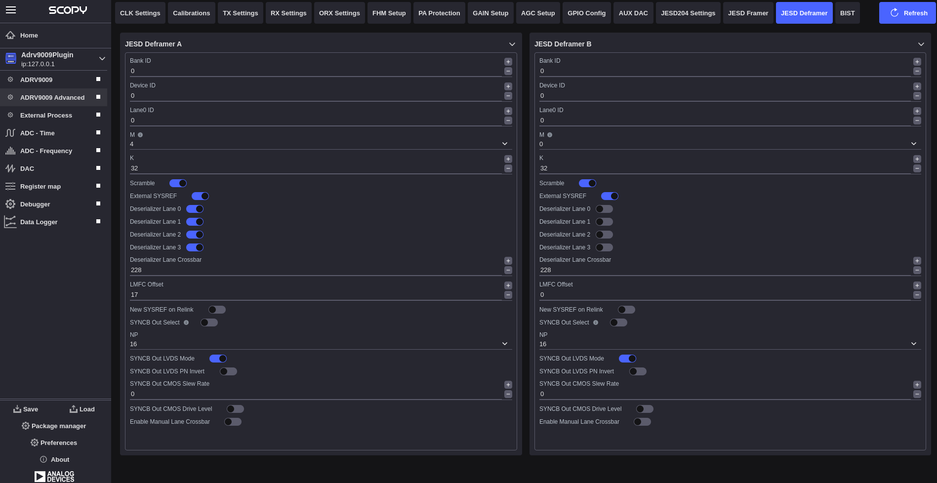
- JESD Deframer A (21 attributes):
Bank ID: Range [0-15]
Device ID: Range [0-255]
Lane0 ID: Range [0-31]
M: Number of converters [0,2,4]
K: Frames per multiframe [1-32]
F: Bytes per frame [1,2,3,4,6,8]
NP: Sample resolution [12,16,24]
Scramble: Enable/disable scrambling
External SYSREF: System reference control
Deserializer Lane 0-3: Individual lane controls
Deserializer Lane Crossbar: Crossbar configuration
LMFC Offset: Local multiframe clock offset
New SYSREF on Relink: Relink control
SYNCB Out Select: SYNCB output selection
Enable Auto Channel Selection: Auto channel control
Additional deserializer and configuration controls
- JESD Deframer B (21 attributes):
Similar deframer configuration for second deframer path
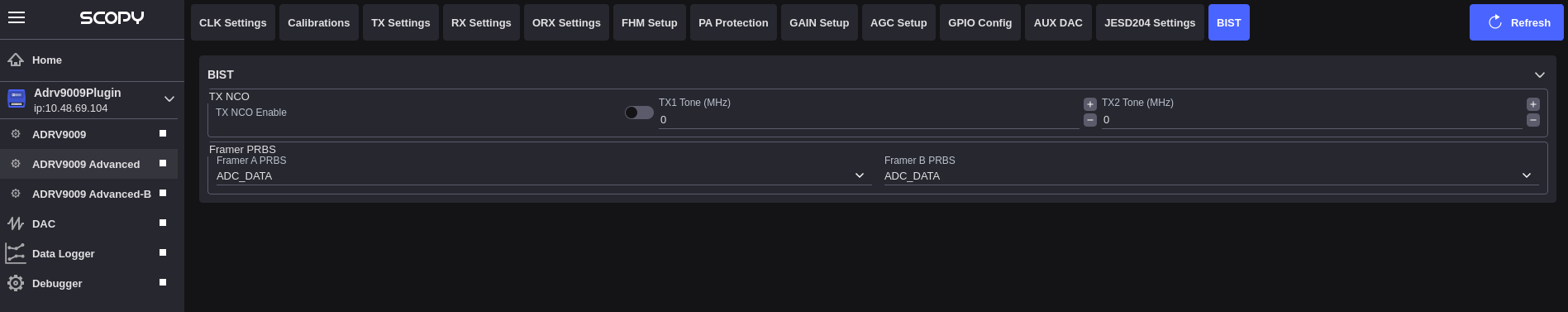
BIST (Built-In Self Test)
The BIST section provides built-in self-test capabilities implemented as part of the calibration_bist branch:
BIST Configuration: Built-in self-test pattern selection and configuration controls for device validation and diagnostics.
Troubleshooting
- Configuration Issues:
Verify device profile compatibility before loading configurations
Check for conflicting settings between basic and advanced plugins
Ensure proper calibration completion before advanced configuration
- Performance Issues:
Monitor device temperature during advanced operations
Verify power supply stability for optimal performance
Check JESD204 link status for data path issues
- Calibration Problems:
Allow adequate warm-up time before running calibrations
Ensure proper RF signal conditions during calibration
Monitor calibration convergence and completion status