A Precision Converter FPGA Integration Journey
This workshop goes through the whole stack for the integration of a precision converter using an FPGA, demonstrating how to achieve maximum performance with the SPI Engine Framework.
Prerequisites
Before starting this workshop, you should have:
Basic understanding of FPGA development concepts
Familiarity with SPI protocol fundamentals
Access to the following resources:
Hardware:
Cora Z7S development board
EVAL-AD7984-PMDZ evaluation board
SD Card
ADALM2000 for testing
Software
Access to a Linux machine or WSL
ADI Kuiper Imager or a similar tool for flashing an OS image onto an SD card
PuTTY or a similar tool for serial communication
If you are working from WSL, you will need the usbipd-win utility to attach a usb port to the Linux environment
Note
The steps presented in this workshop were created using a Windows based machine and WSL.
Learning Objectives
By the end of this workshop, you will:
Understand why traditional MCU SPI controllers limit converter performance
Learn the SPI Engine Framework architecture and components
Build a complete AD7984 precision converter system
Compare regular SPI vs. SPI Engine performance metrics
Achieve near-datasheet performance with proper FPGA integration
Introduction
Customer Journey
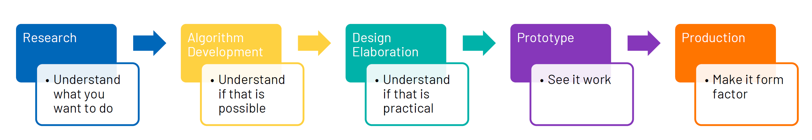
Figure 1 Customer development journey: ADI provides reference designs that port to current development environments and evaluation kits.
Note
Tools and platforms are a customer choice. ADI maintains reference designs across multiple FPGA vendors and development boards to support diverse needs.
Figure 2 Maintenance lifecycle: Customers start designs at different times and require access to the latest tools and IP cores.
Reference Design “Donut Hole” Strategy
The strategy focuses on surrounding customer-selected processors, FPGAs, and microcontrollers with ADI components, creating a seamless integration experience.
Key Benefits:
- Low Friction:
Customers experience minimal integration effort
- Ecosystem Leverage:
Participation in thriving open-source communities
- Design Stickiness:
Reference designs encourage continued ADI component usage
- Community Support:
Access to massive user bases across platforms
Ecosystem Scale:
Linux kernel: 1.3 Billion users
GitHub: 40 Million users
Python: 100 Million users
MATLAB: 1 Million users
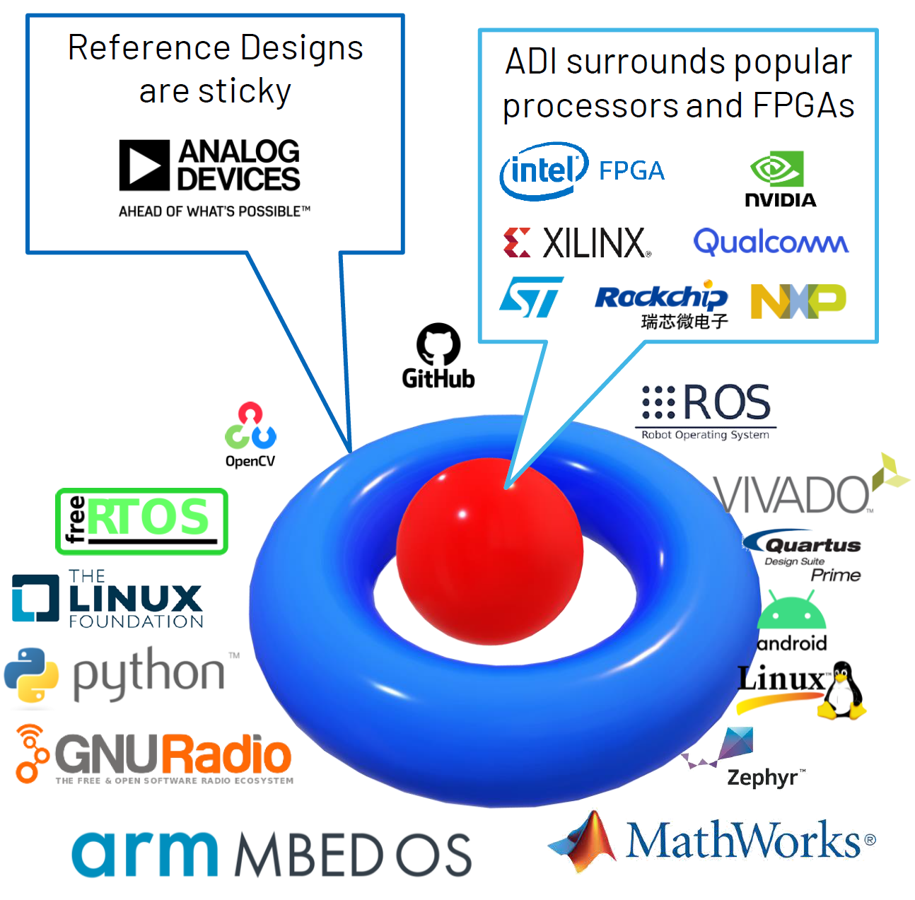
Figure 3 The “Donut Hole” strategy: ADI surrounds customer technology choices with comprehensive hardware and software support, enabling rapid development.
Full Stack High Level Overview
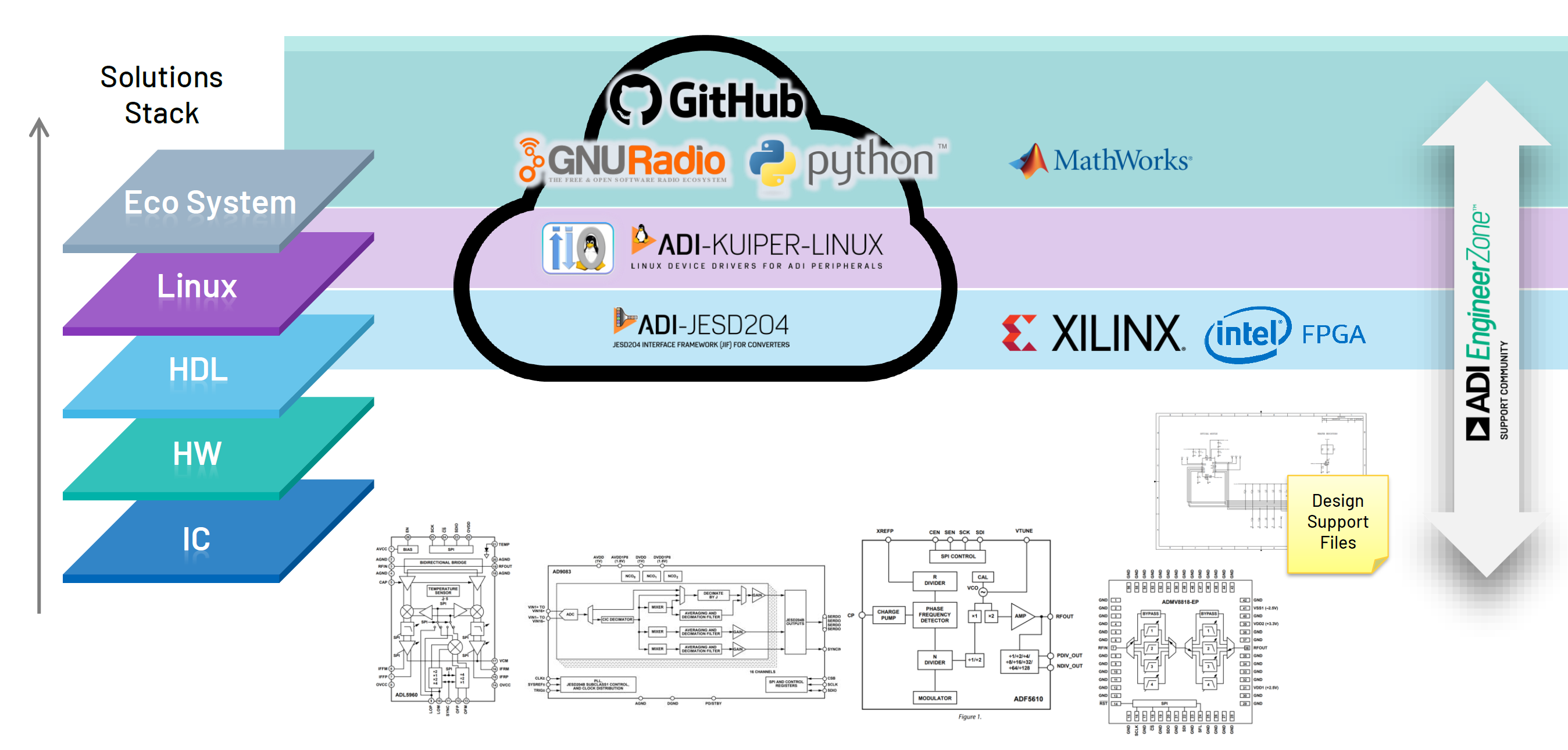
Figure 4 Complete system architecture showing the full software and hardware stack from applications down to FPGA HDL and ADI converters.
Full Stack HDL Designs
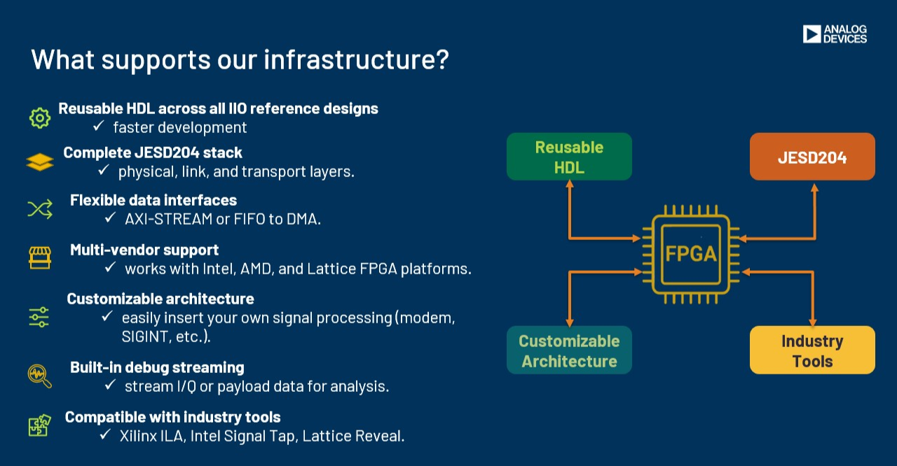
Figure 5 Complete infrastructure diagram showing the full stack HDL design architecture.
Typical Prototyping System
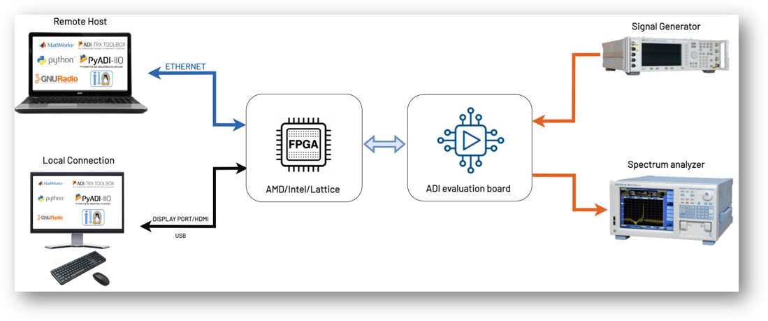
Figure 6 Infrastructure components and tools that support ADI’s reference design ecosystem, including development environments, build systems, and deployment platforms.
Supported FPGA Platforms:
Vendor |
Supported Platforms |
|---|---|
AMD/Xilinx |
Zynq-7000 | VersalAI Core | Virtex UltraScale+ | Versal Prime Series | Versal Premium | Zynq UltraScale+ |
Intel/Altera |
Arria 10 SoC | Stratix 10 SoC | Cyclone 5 SoC | Agilex 7 I-Series |
Lattice |
CertusPro-NX |
IP Library
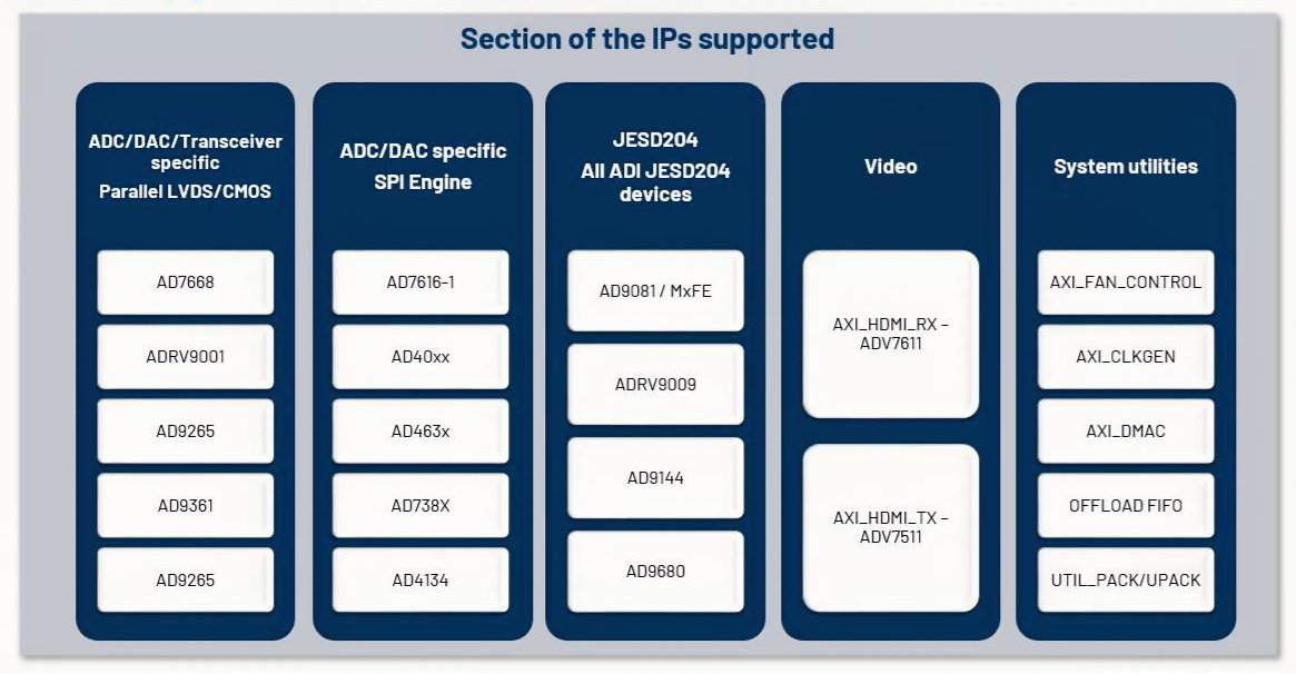
Figure 7 ADI’s open-source IP library provides reusable HDL cores for common functions including DMAs, interfaces, utilities, and converter-specific IP blocks.
Frameworks - JESD204 Interface Framework
The JESD204 framework provides a complete solution for high-speed converter interfaces.
JESD204 Layer Architecture:
- Physical Layer:
FPGA-specific transceivers (GTXE2, GTHE3, GTHE4, GTY4, GTY5, Arria 10, Stratix 10)
- Data Link Layer:
Available under GPL 2 and commercial license
- Transport Layer:
Converter-specific implementations for ADCs, DACs, and transceivers
Complete Framework Includes:
Evaluation boards with FMC connectivity
Production-ready HDL IP cores
Linux device drivers and software APIs
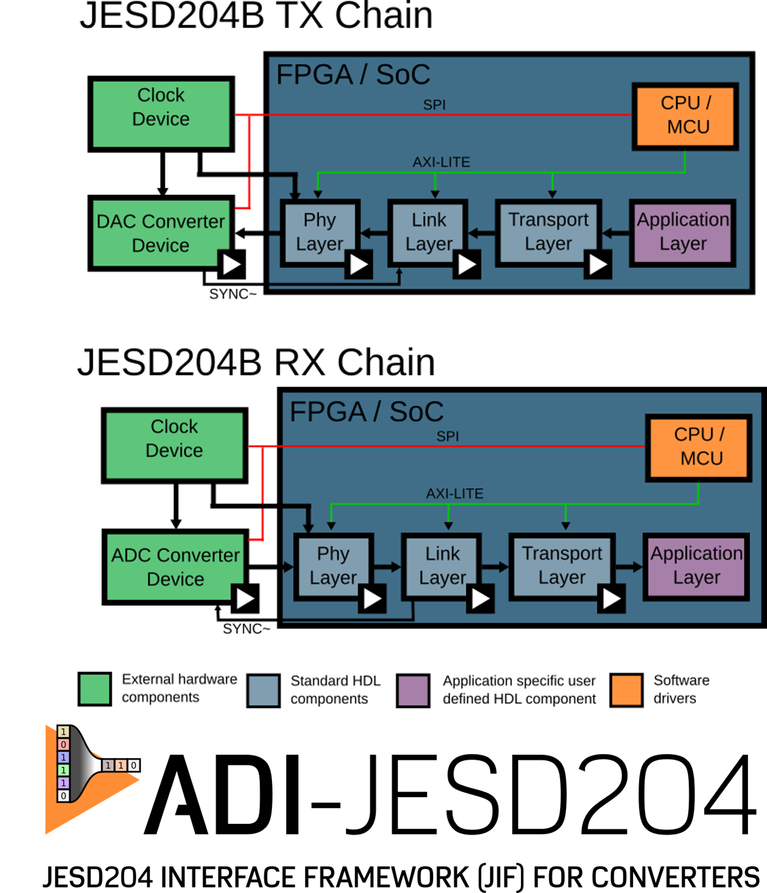
Figure 8 JESD204 signal chain showing all three layers from FPGA transceiver through data link processing to converter-specific transport.
Frameworks - SPI Engine Framework
Tip
SPI Engine Powers Over 20% of ADI’s HDL Projects
The SPI Engine framework is a critical component for precision converter integration, supporting a wide range of SAR ADCs and other SPI devices.
HDL Project Distribution:
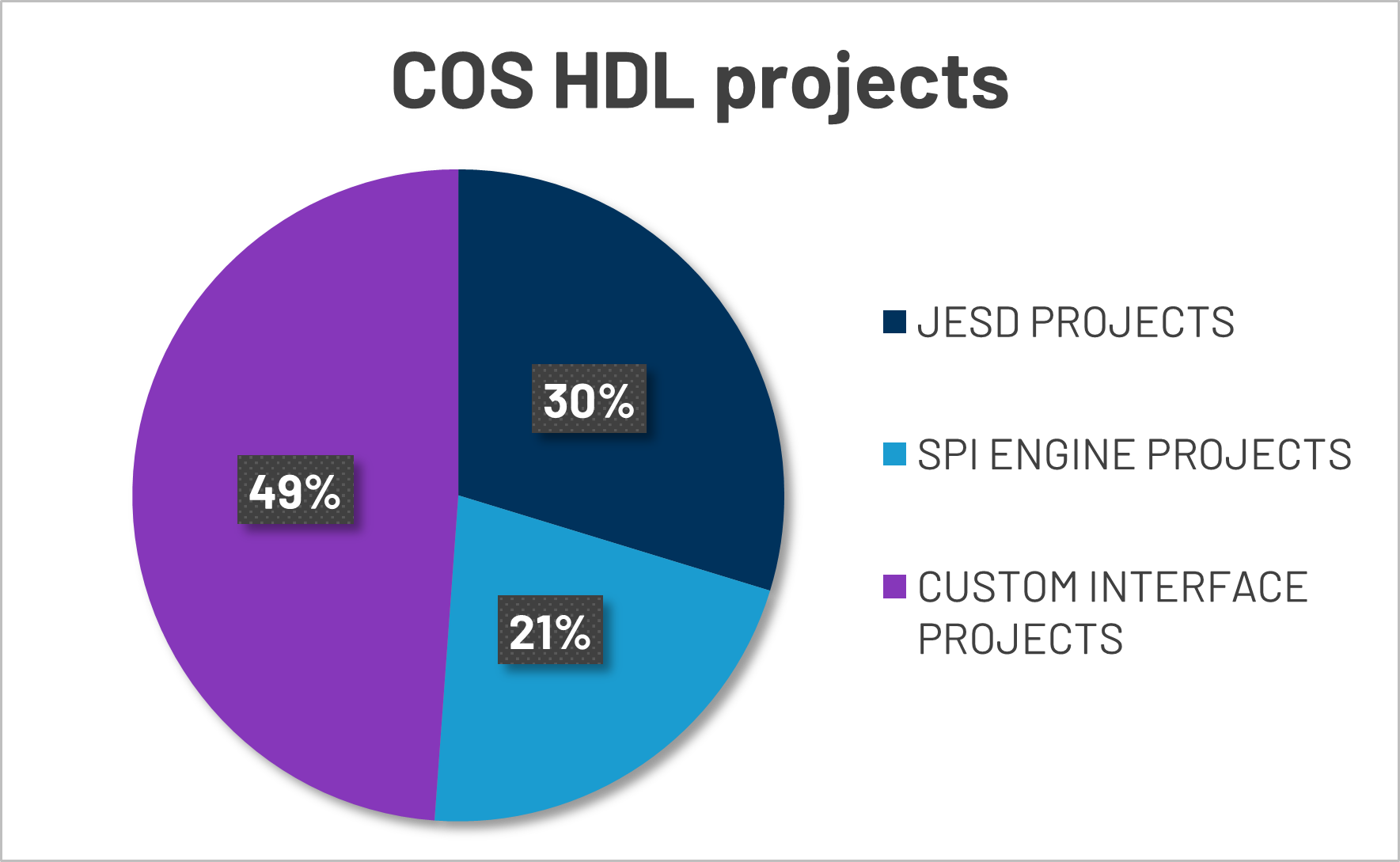
Figure 9 Distribution of HDL projects by interface type: JESD204 (34%), SPI Engine (21%), and Custom Interfaces (45%).
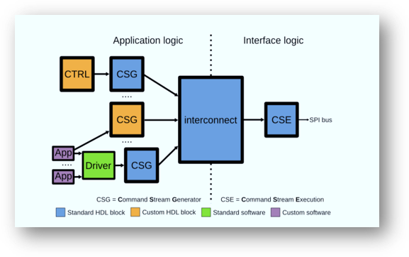
Figure 10 SPI Engine framework icon representing the modular, flexible architecture for precision converter interfaces.
SPI Engine Framework Modules:
- AXI SPI Engine (CSG):
Core SPI interface with memory-mapped control
- Offload Engine (CSG):
Efficient autonomous data handling and streaming
- Interconnect:
Bridges application and interface logic with arbitration
- Execution Engine (CSE):
Command stream execution and physical SPI signal generation
Framework Includes:
ADC/DAC support: Extensive library of precision converter drivers
HDL components: Standard and custom IP blocks for AMD Xilinx and Intel FPGAs
Software support: Bare-metal APIs and Linux kernel driver integration
SPI Engine Architecture
Serial Peripheral Interface (SPI) - Background
SPI is a full-duplex serial communication bus designed by Motorola in the mid-1980s. It is widely used for short-distance chip-to-chip communication in embedded systems and has become a de facto industry standard despite small variations across implementations.
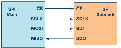
Figure 11 Basic SPI interface showing master-slave connection with four signal lines.
SPI Signal Definitions:
- SCLK:
Serial Clock from master (sets transfer rate)
- MOSI:
Master Output Slave Input (data from master to slave)
- MISO:
Master Input Slave Output (data from slave to master)
- CSN:
Chip Select N, active low (enables specific slave device)
SPI Operating Modes:
SPI supports four operating modes based on two configuration bits: CPOL (Clock Polarity) and CPHA (Clock Phase).
Mode |
CPOL |
CPHA |
Description |
|---|---|---|---|
Mode 0 |
0 |
0 |
Clock idle LOW, data sampled on RISING edge, shifted on falling edge |
Mode 1 |
0 |
1 |
Clock idle LOW, data sampled on FALLING edge, shifted on rising edge |
Mode 2 |
1 |
0 |
Clock idle HIGH, data sampled on FALLING edge, shifted on rising edge |
Mode 3 |
1 |
1 |
Clock idle HIGH, data sampled on RISING edge, shifted on falling edge |
SPI Mode Timing Diagrams:
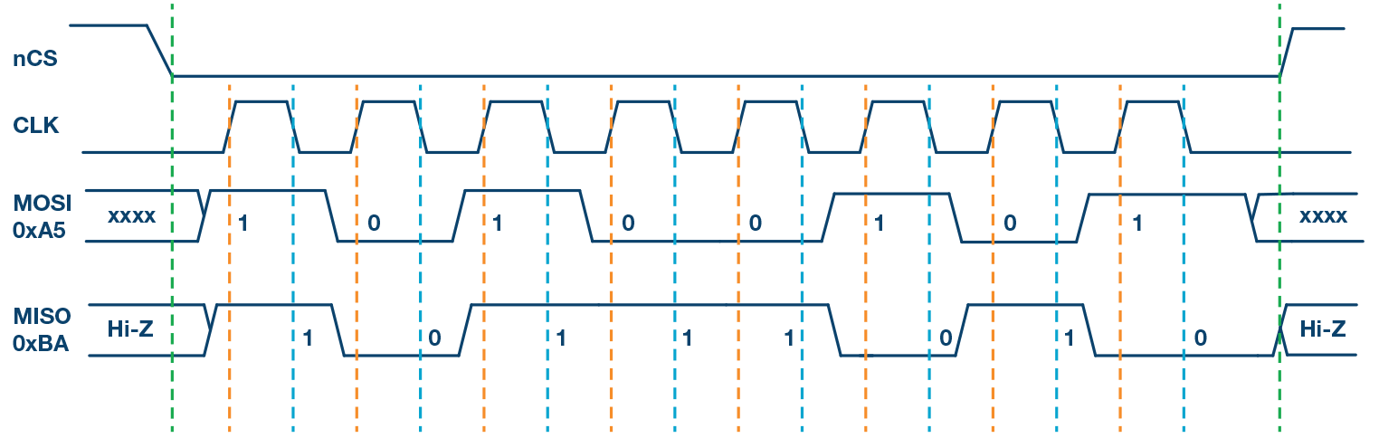
Figure 12 Mode 0 (CPOL=0, CPHA=0) - Most Common Mode: Clock idles LOW, data sampled on RISING edge
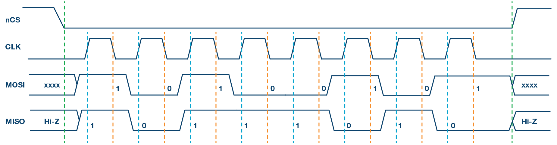
Figure 13 Mode 1 (CPOL=0, CPHA=1): Clock idles LOW, data sampled on FALLING edge
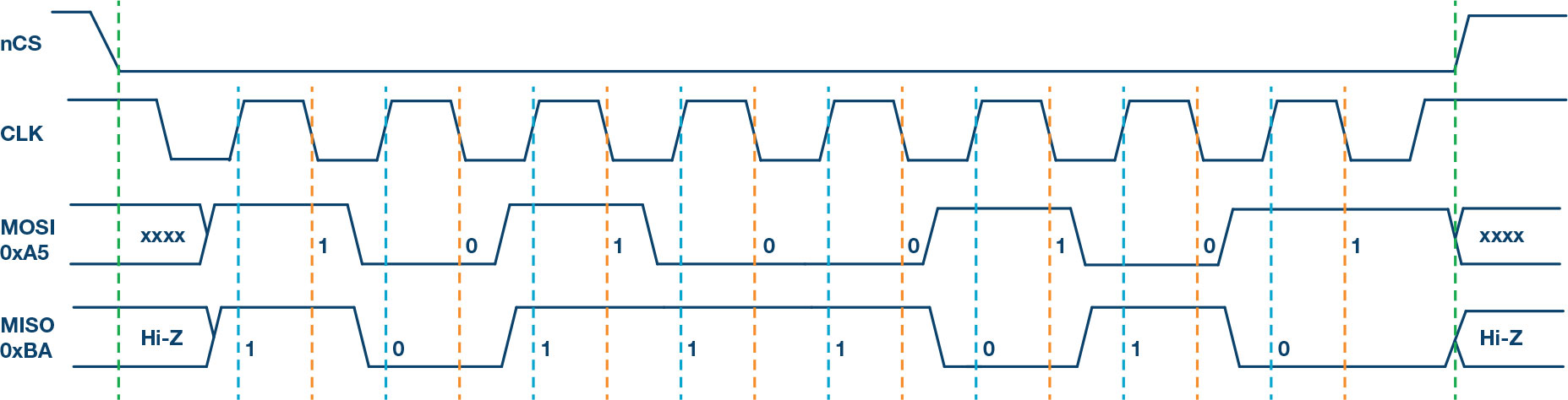
Figure 14 Mode 2 (CPOL=1, CPHA=0): Clock idles HIGH, data sampled on FALLING edge
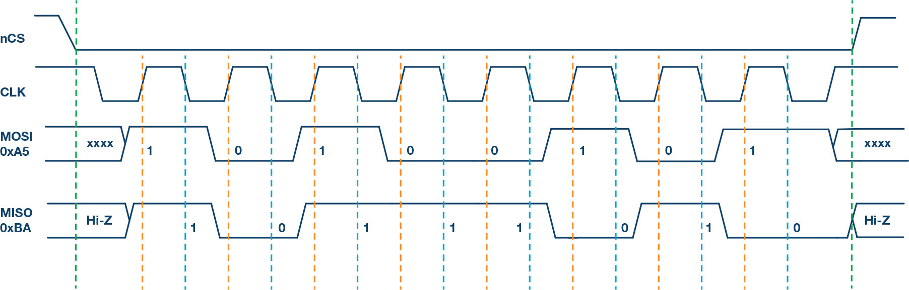
Figure 15 Mode 3 (CPOL=1, CPHA=1): Clock idles HIGH, data sampled on RISING edge
Why MCU SPI Controllers Are Not Sufficient for Precision Converters
Important
Critical Limitation: MCU SPI Controllers Cannot Achieve Datasheet Performance
Traditional MCU SPI controllers introduce timing jitter and limit sampling rates, preventing precision converters from reaching their full potential.
Physical Layer Limitations:
3-wire SPI support (less common than 4-wire)
CS often serves dual purposes (chip select AND conversion trigger)
No support for additional control lines (BUSY, CNV)
Single MOSI/MISO line limitation
SCLK frequency limited to ~50MHz (higher speeds rare)
Fixed timing relationships between interface signals
No synchronization capability with external signals
No DDR (double data rate) support
Software-Driven Performance Issues:
- High Latency:
Software overhead prevents fast response times
- No Streaming:
Cannot support continuous high-throughput data capture
- Non-Deterministic:
Time between function call and actual transfer is variable
- CPU Overhead:
Processor must manage every transfer, limiting system performance
Attention
The combination of these limitations means MCU SPI controllers typically achieve only 15-20% of a converter’s datasheet performance specifications!
SPI Transfer Timing Examples
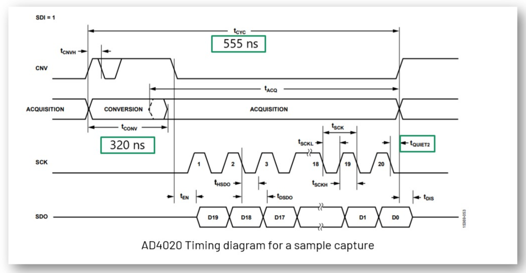
Figure 16 AD4020 SPI timing diagram showing the precise timing requirements for CNV pulse, conversion time, and data readback for this 20-bit, 1.8 MSPS converter.
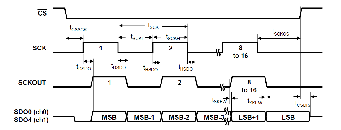
Figure 17 AD4630 SPI timing diagram illustrating dual-channel simultaneous sampling with specific timing constraints for this 24-bit, 2 MSPS differential ADC.
SPI Engine Framework – The Solution
Note
Open-Source, Production-Ready Framework
SPI Engine is a highly flexible and powerful open-source SPI controller framework specifically designed to overcome the limitations of traditional SPI controllers.
The framework consists of multiple submodules that communicate over well-defined interfaces, enabling high flexibility and reusability while remaining highly customizable and easily extensible.
Key Framework Features:
- Multi-Vendor HDL:
Supports both AMD Xilinx and Intel FPGAs
- Linux Integration:
Fully integrated into the Linux kernel SPI framework
- Bare-Metal Support:
Standalone API for RTOS and bare-metal applications
- Production Ready:
Extensively tested with numerous ADI converters
- Open Source:
Available on GitHub with active community support
Benefits Over Traditional SPI:
Hardware-driven transfers with deterministic timing
Support for high-speed continuous streaming (>100 MSPS data rates)
Sub-microsecond latency for conversion triggers
Flexible timing control to meet any converter’s requirements
Simultaneous support for multiple SPI devices
SPI Engine Framework – HDL Architecture
The SPI Engine uses a modular architecture with three main components communicating via standardized AXI-Stream interfaces.
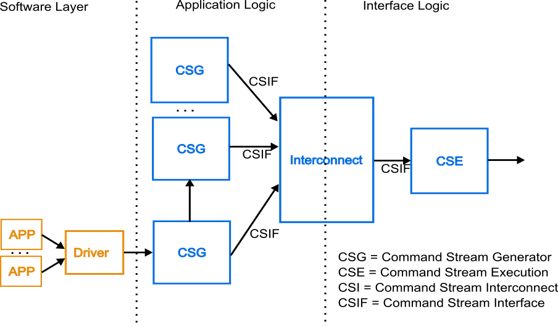
Figure 18 Complete SPI Engine framework architecture showing the three main components: Command Stream Generator (CSG), Interconnect (CSI), and Executor (CSE).
Component Descriptions:
- Command Stream Generator (CSG)
Generates SPI command sequences. Can operate in multiple modes:
Software driven: Controlled through memory-mapped registers
Hardware driven: Triggered by external events for data offload
Periodic: Generates commands at fixed intervals
Synchronous: Responds to external trigger signals
- Command Stream Executor (CSE)
Parses incoming command streams and drives the physical SPI pins.
Standard parser for common SPI protocols
Customizable for special requirements (e.g., custom SDI latching)
Handles all SPI modes and timing configurations
- Command Stream Interconnect (CSI)
Arbitrates multiple command streams to a single executor.
Supports multiple CSGs sharing one physical SPI interface
Priority-based arbitration (lower port number = higher priority)
Transaction-level switching (uses SYNC instruction)
SPI Engine Framework – AXI SPI Engine IP
The AXI SPI Engine IP provides the memory-mapped interface for software control and configuration.
Key Features:
Memory-mapped access to command stream interface (fully software-controlled CSG)
Memory-mapped access to offload control for dynamic reconfiguration
Asynchronous clock domains (SPI clock independent of AXI clock)
FIFO buffers for command, SDO, and SDI data
Interrupt support for transfer completion
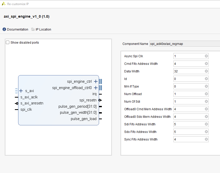
Figure 19 AXI SPI Engine IP block diagram showing register interface, FIFOs, and connections to the SPI Engine execution core.
SPI Engine Framework – Data Offload IP
The Data Offload module enables autonomous, hardware-triggered SPI transfers without CPU intervention, critical for high-performance streaming applications.
Offload Capabilities:
Internal RAM/ROM stores command sequences and SDO data
External trigger launches predefined command stream
Received SDI data streams directly to AXI4-Stream interface
Direct DMA connection for zero-copy data transfer
Supports continuous, periodic sampling at maximum rates
Tip
The offload module is essential for achieving 1+ MSPS with precision converters, as it eliminates all software latency and CPU overhead.
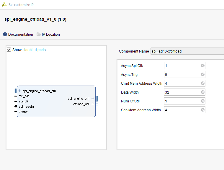
Figure 20 Data Offload IP showing trigger input, command/data storage, and streaming output for autonomous high-speed operation.
SPI Engine Framework – Interconnect IP
The Interconnect enables multiple command sources to share a single physical SPI interface, useful when mixing software-controlled and hardware-offloaded transfers.
Interconnect Features:
Arbitrates multiple command streams to one executor
Transaction-level arbitration (complete SPI transfers are atomic)
SYNC instruction marks transaction boundaries
Priority-based: Lower slave port number = higher priority
No command stream fragmentation
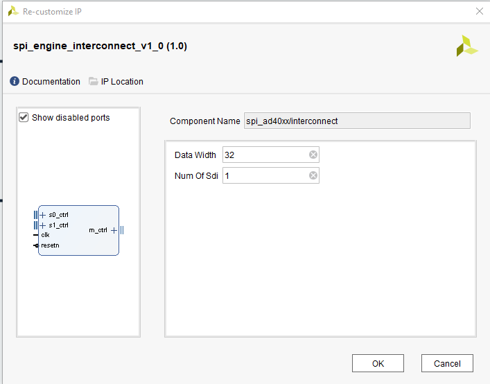
Figure 21 Interconnect IP showing multiple input ports with priority arbitration to a single output feeding the execution module.
SPI Engine Framework – Execution IP
The Execution module is the physical layer that converts command streams into actual SPI signal transitions with precise timing control.
Execution Features:
Accepts commands on the AXI-Stream control interface
Generates low-level SPI signals (SCLK, MOSI, MISO, CS)
Active signal indicates busy status during command processing
Configurable for all SPI modes (0-3)
Supports variable word lengths and transfer delays
Precise timing control for converter-specific requirements
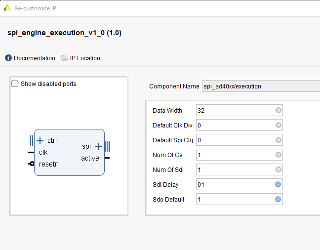
Figure 22 Execution IP showing command stream input, timing control, and physical SPI signal outputs with precise waveform generation.
SPI Engine Framework – Command Stream Interfaces
The framework uses four dedicated AXI-Stream interfaces for different data types:
- CMD:
Command/instruction stream
- SDO:
SPI write data stream (Master Output, Slave Input / MOSI)
- SDI:
SPI read data stream (Master Input, Slave Output / MISO)
- SYNC:
Synchronization event stream
Interface Characteristics:
Standard AXI-Stream handshaking protocol (ready, valid, data signals)
Allows independent flow control for each stream
Enables efficient pipelining and buffering
Simple, well-defined interface for custom IP integration
SPI Engine Framework – Software Support
The framework introduces comprehensive SPI offload capabilities to Linux and bare-metal systems.
Offload Concept:
Moves converter-specific operations from the application processor to dedicated hardware, dramatically improving performance and reducing CPU load.
Software Features:
- Interrupt Offload:
Hardware manages conversion timing and interrupts
- Data Offload:
Direct DMA transfers bypass CPU entirely
- Universal API:
ADI converter drivers work with any offload-capable SPI controller
- Linux Integration:
Part of standard kernel SPI framework (drivers/spi/spi-axi-spi-engine.c)
- Bare-Metal Support:
Standalone API for embedded applications
Note
Once an ADI converter driver is written for SPI Engine, it can be used with any other offload-capable SPI controller with minimal changes.
Use Case: High-Performance AD7984 Integration
Application Requirements
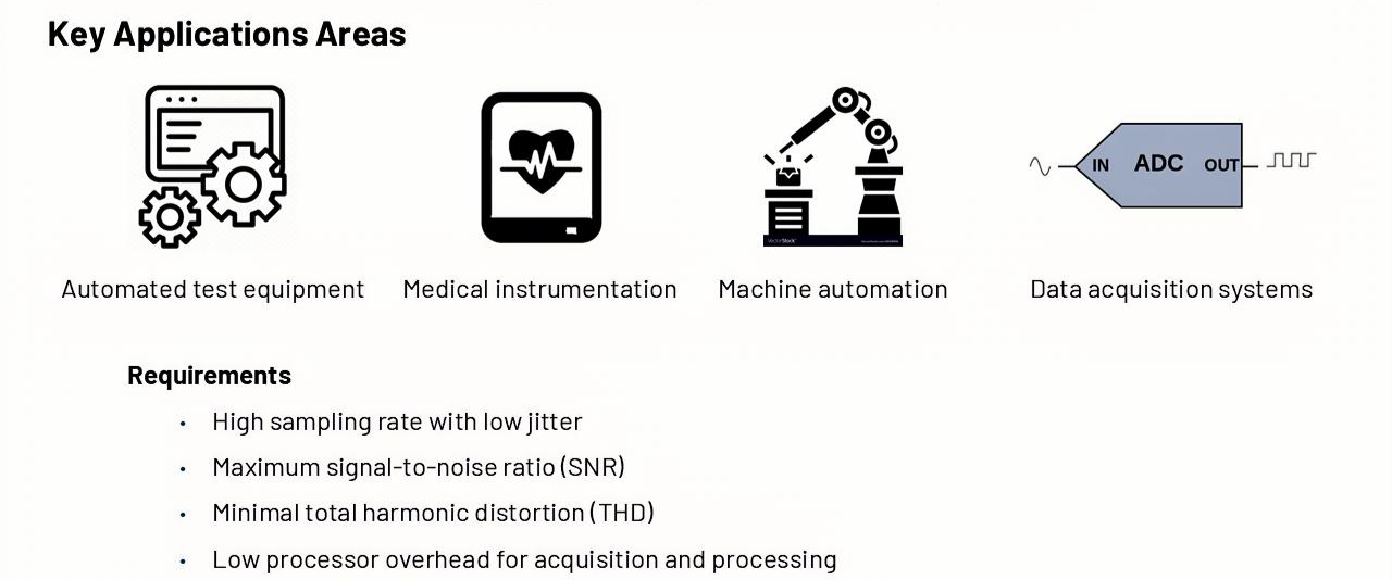
Figure 23 Target applications including medical imaging, industrial automation, and precision measurement systems requiring high-fidelity data acquisition.
System Performance Goals:
Important
Critical Requirements for Precision Measurement
- Maximum Sample Rate:
Achieve full 1.33 MSPS with low jitter
- Maximum SNR:
Reach datasheet specifications (98.5 dB)
- Minimum THD:
Achieve -110 dB total harmonic distortion
- Low CPU Overhead:
Minimize processor usage for sustained operation
Test Configuration Comparison:
Test Condition |
Regular SPI |
SPI Engine |
|---|---|---|
Resolution (bits) |
16 |
18 (full converter resolution) |
Sampling Rate (KSPS) |
15 (limited) |
15 and 1330 (full rate) |
Input Frequency (kHz) |
1 |
1 |
Input Amplitude (dBFS) |
-0.5 |
-0.5 |
Supply Voltage (V) |
±2.5 and +5 |
±2.5 and +5 |
AD7984: High-Performance 18-bit SAR ADC
The AD7984 is an ideal choice for demonstrating SPI Engine capabilities due to its demanding timing requirements and excellent specifications.
See also
Key Specifications:
- Resolution:
18 bits with no missing codes
- Sample Rate:
1.33 MSPS (maximum throughput)
- Architecture:
Zero-latency SAR with internal reference
- Input Range:
True differential ±VREF or single-ended 0 to VREF (2.9 V to 5 V)
AC Performance (at fIN = 1 kHz, VREF = 5 V):
SNR: 98.5 dB
THD: -110.5 dB
SINAD: 97.5 dB
Dynamic Range: 99.7 dB
Tip
These excellent specifications can only be achieved with proper FPGA-based timing control. MCU SPI controllers cannot maintain the required precision.
AD7984 SPI Transfer Timing Diagram
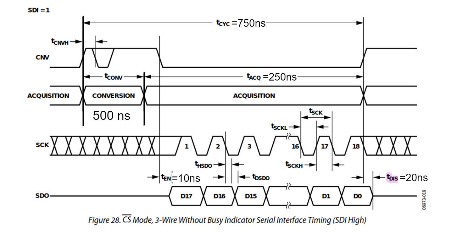
Figure 24 Detailed timing diagram showing CNV pulse width, acquisition time, conversion time, and SPI data readback requirements for the AD7984.
Timing Parameters for SPI Engine Configuration
The SPI Engine framework supports a wide range of precision converters. This table shows the key timing parameters needed for configuration.
Device |
Resolution (bits) |
Sample Rate (KSPS) |
T_SPI_SCLK min (ns) |
T_CONV max (ns) |
T_CYC min (ns) |
T_ACQ min (ns) |
|---|---|---|---|---|---|---|
AD7942 |
14 |
250 |
18 |
2200 |
4000 |
1800 |
AD7946 |
14 |
500 |
15 |
1600 |
2000 |
400 |
AD7988-1 |
16 |
100 |
12 |
9500 |
1000 |
500 |
AD7685 |
16 |
250 |
15 |
2200 |
4000 |
1800 |
AD7687 |
16 |
250 |
10 |
2200 |
4000 |
1800 |
AD7691 |
16 |
250 |
15 |
2200 |
4000 |
1800 |
AD7686 |
16 |
500 |
15 |
1600 |
2000 |
400 |
AD7693 |
16 |
500 |
15 |
1600 |
2000 |
400 |
AD7988-5(B) |
16 |
500 |
12 |
1600 |
2000 |
400 |
AD7988-5(C) |
16 |
500 |
12 |
1200 |
2000 |
800 |
AD7980 |
16 |
1000 |
10 |
710 |
1000 |
290 |
AD7983 |
16 |
1333 |
12 |
500 |
750 |
250 |
AD7982 |
18 |
1000 |
12 |
710 |
1000 |
290 |
AD7984 |
18 |
1333 |
12 |
500 |
750 |
250 |
Note
AD7984 (highlighted) is used in this workshop due to its high sample rate (1.33 MSPS), 18-bit resolution, and demanding timing requirements that showcase SPI Engine capabilities.
HDL Design Block Diagram
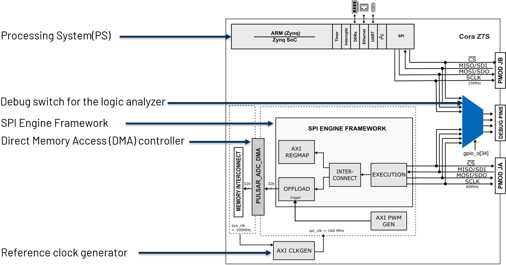
Figure 25 Complete HDL block diagram showing SPI Engine framework integration with PWM trigger generator, clock generation, DMA, and processor interface.
HDL Framework Instantiation
The SPI Engine framework provides a TCL helper function to simplify instantiation.
TCL Function Signature:
proc spi_engine_create {{name "spi_engine"} {data_width 32} {async_spi_clk 1} {num_cs 1} {num_sdi 1} {sdi_delay 0} {echo_sclk 0}}
Instantiation Example for PulSAR ADC Family:
1source $ad_hdl_dir/library/spi_engine/scripts/spi_engine.tcl
2set data_width 32
3set async_spi_clk 1
4set num_cs 1
5set num_sdi 1
6set sdi_delay 1
7set hier_spi_engine spi_pulsar_adc
8spi_engine_create $hier_spi_engine $data_width $async_spi_clk $num_cs $num_sdi $sdi_delay
Parameter Descriptions:
- DATA_WIDTH:
Sets the data bus width for DMA connection and maximum SPI word length. For PulSAR ADCs with up to 18-bit transfers, use 32 bits.
- ASYNC_SPI_CLK:
Selects the SPI Engine reference clock:
0: Use AXI clock (100 MHz)1: Use external SPI_CLK for independent timing control (recommended)
- NUM_CS:
Number of chip select lines (typically 1 for single converter)
- NUM_SDI:
Number of SDI (MISO) lines for multi-lane interfaces
- SDI_DELAY:
SDI latch delay in SPI clock cycles (1, 2, or 3). Required for high-speed designs with SCLK > 50 MHz to meet setup/hold timing.
PulSAR ADC Architecture
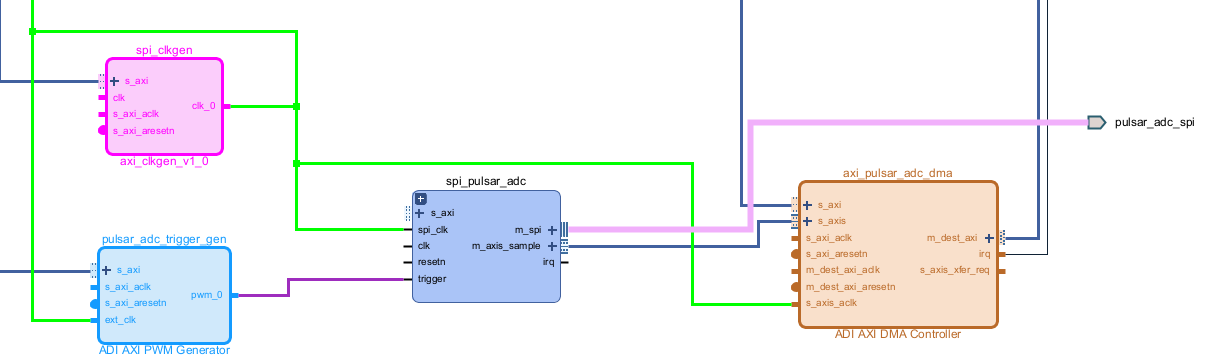
Figure 26 Complete system architecture for PulSAR ADC integration showing PWM trigger generator, SPI Engine with offload, clock generation, and DMA controller.
ad_ip_parameter pulsar_adc_trigger_gen CONFIG.PULSE_0_PERIOD 120
ad_ip_parameter pulsar_adc_trigger_gen CONFIG.PULSE_0_WIDTH 1
ad_connect spi_clk pulsar_adc_trigger_gen/ext_clk
ad_connect pulsar_adc_trigger_gen/pwm_0 $hier_spi_engine/offload/trigger
ad_ip_instance axi_clkgen spi_clkgen
ad_ip_parameter spi_clkgen CONFIG.CLK0_DIV 5
ad_ip_parameter spi_clkgen CONFIG.VCO_DIV 1
ad_ip_parameter spi_clkgen CONFIG.VCO_MUL 8
ad_connect $hier_spi_engine/m_spi pulsar_adc_spi
ad_connect spi_clk spi_clkgen/clk_0
ad_connect spi_clk spi_pulsar_adc/spi_clk
ad_ip_parameter axi_pulsar_adc_dma CONFIG.DMA_TYPE_SRC 1
ad_ip_parameter axi_pulsar_adc_dma CONFIG.DMA_TYPE_DEST 0
ad_ip_parameter axi_pulsar_adc_dma CONFIG.CYCLIC 0
ad_ip_parameter axi_pulsar_adc_dma CONFIG.SYNC_TRANSFER_START 0
ad_ip_parameter axi_pulsar_adc_dma CONFIG.AXI_SLICE_SRC 0
ad_ip_parameter axi_pulsar_adc_dma CONFIG.AXI_SLICE_DEST 1
ad_ip_parameter axi_pulsar_adc_dma CONFIG.DMA_2D_TRANSFER 0
ad_ip_parameter axi_pulsar_adc_dma CONFIG.DMA_DATA_WIDTH_SRC 32
ad_ip_parameter axi_pulsar_adc_dma CONFIG.DMA_DATA_WIDTH_DEST 64
ad_connect spi_clk axi_pulsar_adc_dma/s_axis_aclk
Test System Setup
Overview
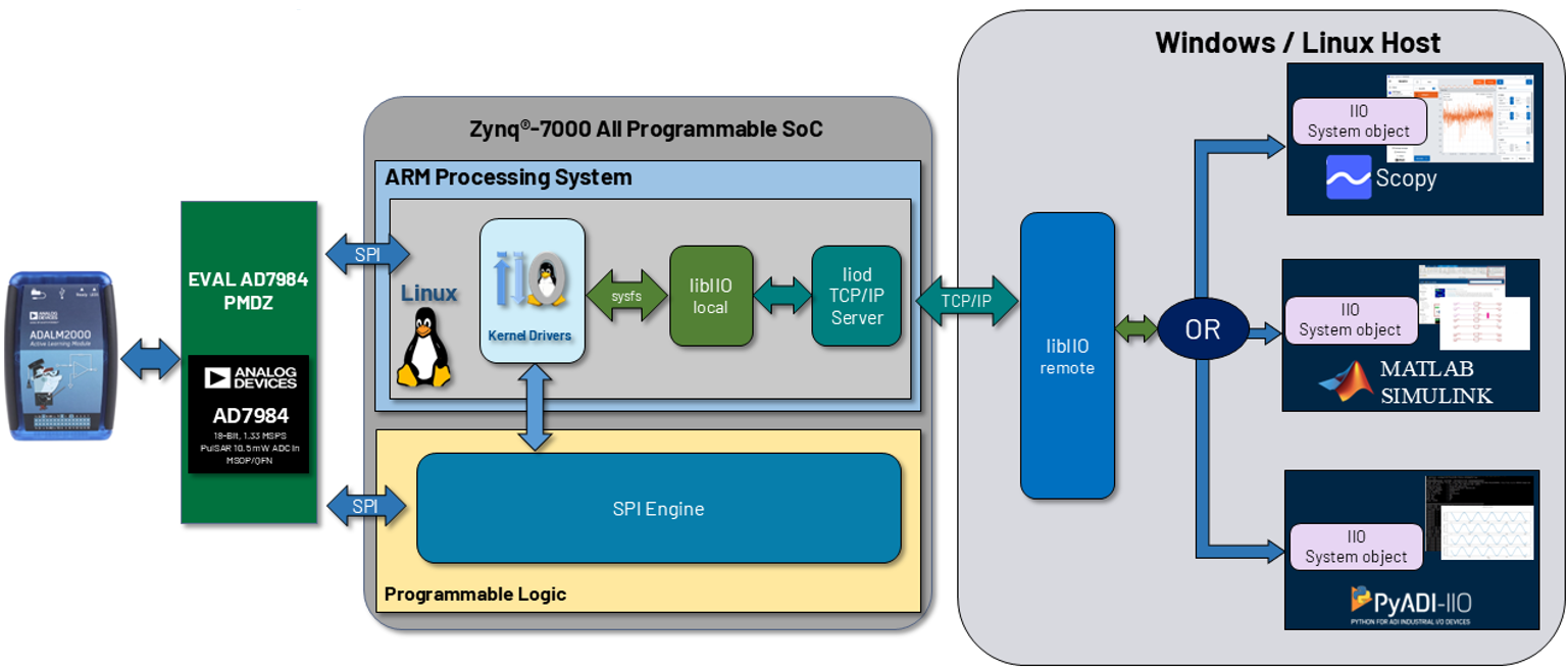
Figure 27 Complete workshop system showing Cora Z7S FPGA board, AD7984 converter circuit, ADALM2000 for signal generation and debug, and host computer.
Repository and Build Environment Setup
Follow these steps to set up your development environment with the necessary repositories and toolchain:
Step 1: Create Workspace Directory
Create a folder to store the temporary files for the workshop:
cd ~
mkdir spi_workshop
cd spi_workshop/
Important
The location of this directory will be used throughout the entire workshop. If you chose a different location for your directory, make sure to replace the path from the examples with your path.
Step 2: Download Cross-Compiler Toolchain
Download the ARM cross-compiler toolchain for building Linux kernel:
wget https://releases.linaro.org/components/toolchain/binaries/latest-7/arm-linux-gnueabi/gcc-linaro-7.5.0-2019.12-x86_64_arm-linux-gnueabi.tar.xz
tar -xvf gcc-linaro-7.5.0-2019.12-x86_64_arm-linux-gnueabi.tar.xz
Step 3: Set Cross-Compiler Environment Variables
Configure the CROSS_COMPILE and ARCH environment variables:
export CROSS_COMPILE=$(pwd)/gcc-linaro-7.5.0-2019.12-x86_64_arm-linux-gnueabi/bin/arm-linux-gnueabi-
export ARCH=arm
Step 4: Clone HDL Repository and Checkout Branch
Clone the HDL repository and switch to the ad7984_demo branch:
git clone https://github.com/analogdevicesinc/hdl.git
cd hdl
git checkout ad7984_demo
This prepares the HDL project files needed for building the FPGA design.
Step 5: Clone ADI Linux Repository
Clone the Analog Devices Linux kernel repository with device drivers and switch to the ad7984_demo branch:
cd ~/spi_workshop
git clone https://github.com/analogdevicesinc/linux.git
cd linux
git checkout ad7984_demo
This will create a linux directory containing the ADI Linux kernel sources with all necessary drivers.
HDL Project Build Instructions for Zynq Target
Now that you have the repositories set up, follow these guides to build the HDL project and boot image for your Zynq-7000 SoC target (Cora Z7S board):
Step 1: Prepare the SD Card
Use ADI Kuiper Imager (or a similar tool) to flash the SD card with the latest image of ADI Kuiper Linux.
Tip
Here you can find more information about obtaining the latest ADI Kuiper Linux image.
Step 2: Build the HDL Project
Navigate to the pulsar_adc_pmdz project for the Cora Z7S board and build the project:
cd ~/spi_workshop/hdl/projects/pulsar_adc_pmdz/coraz7s
make
Important
If you use a Vivado version higher than 2023.1, the ADI_IGNORE_VERSION_CHECK parameter needs to be set to 1 before building the project:
export ADI_IGNORE_VERSION_CHECK=1
Tip
A comprehensive description of how to build the FPGA HDL design for Zynq platforms, using Vivado, can be found in the Build an HDL project guide, which covers:
Setting up AMD Xilinx Vivado tools for Zynq
Building the FPGA bitstream for Zynq-7000
Generating hardware description files (.xsa)
Zynq-specific build commands and options
Step 3: Build the Zynq Boot Image (BOOT.BIN)
After building the HDL, create the complete Zynq boot image containing FPGA bitstream, FSBL, and U-Boot.
Tip
More information about the process can be found in the Build the boot image BOOT.BIN guide, which covers:
Combining Zynq FSBL, bitstream, and U-Boot into BOOT.BIN
Creating bootable SD card image for Zynq
Devicetree compilation for Zynq-7000 platforms
Boot configuration for ARM processor + FPGA fabric
Note
The u-boot from any of the zynq-coraz7s projects, found on the SD card, can be used to generate the BOOT.BIN file.
Step 4: Build the Zynq Linux Kernel and Devicetree
Build the Linux kernel with ADI drivers and devicetree for Zynq-7000 platforms, using the Linaro toolchain. Navigate to the local copy of the linux repository and confugure the kernel:
cd ~/spi_workshop/linux
make zynq_xcomm_adv7511_defconfig
After successfully configuring the kernel, build the kernel image using the following command:
make -j5 UIMAGE_LOADADDR=0x8000 uImage
Note
Some additional dependecies might be required to successfully build the kernel image. The generated image can be found at ~/spi_workshop/linux/arch/arm/boot/uImage.
Lastly, generate the devicetree using the following command:
make zynq-coraz7s-ad7984.dtb
Note
The devicetree file can be found at ~/spi_workshop/linux/arch/arm/boot/dts/zynq-coraz7s-ad7984.dtb.
Tip
For a detailed overview of the process, check out the Build Zynq Linux kernel and devicetree guide, which covers:
Configuring the Linux kernel for Zynq with ADI device support
Building uImage (kernel) and devicetree blob (DTB)
Cross-compilation setup using the ARM toolchain
Installing kernel modules and preparing rootfs
Complete build commands for Zynq targets
Step 5: Load Files on the SD Card
Copy the BOOT.BIN, uImage, and devicetree files in the root directory of your SD card.
Important
The .dtb file must be renamed to devicetree.dtb before booting.
System Configuration
Schematic
The image below shows the required connections for the hardware setup:
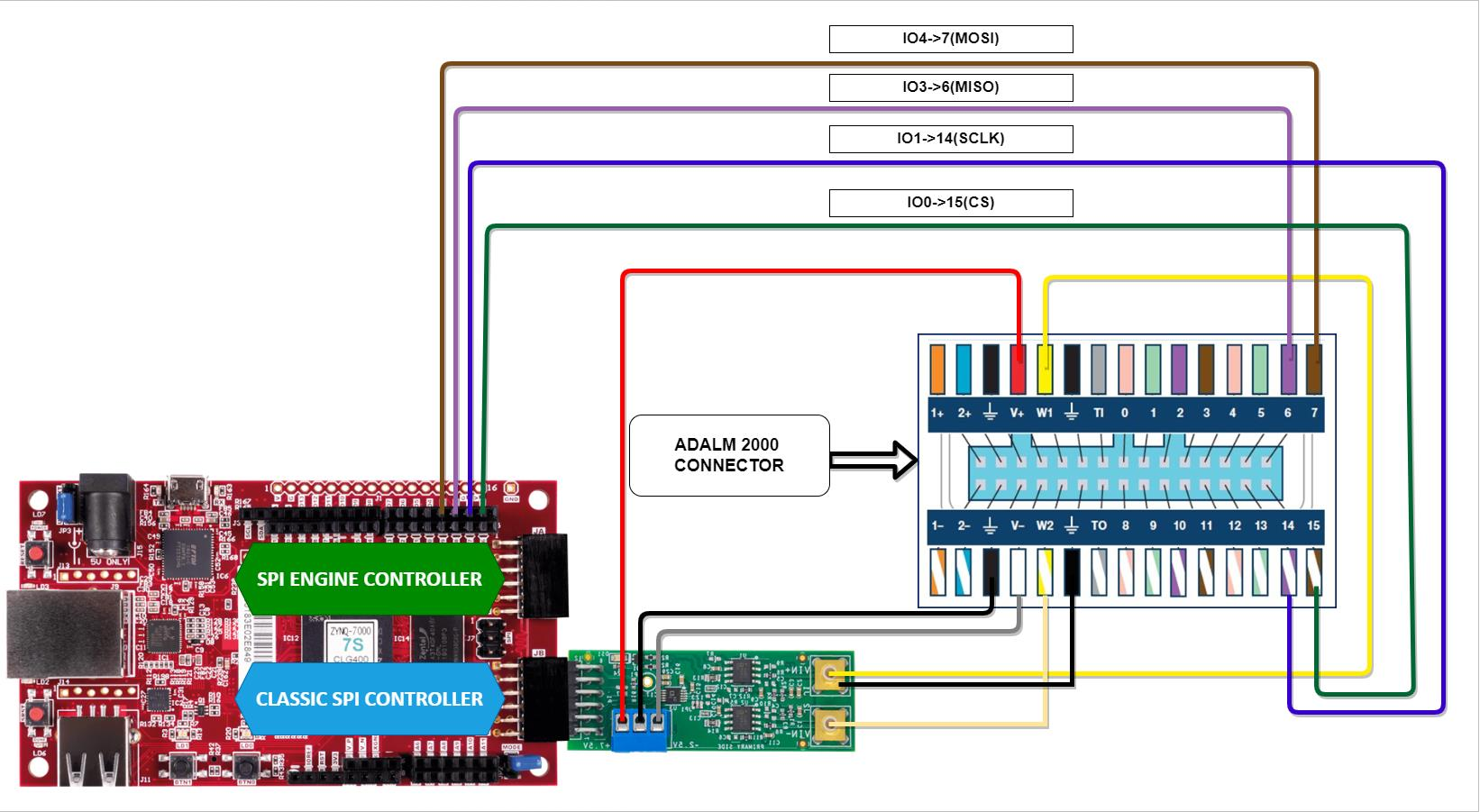
Figure 28 Circuit schematic showing AD7984 connections to Cora Z7S FPGA board, including power, reference, and SPI interface signals.
Cora Z7S Configuration
Follow the steps shown below to power on the Cora development board:
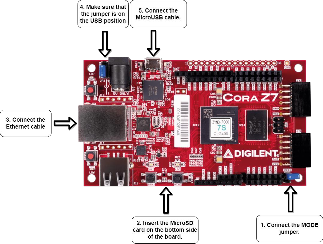
Figure 29 Cora Z7S board setup and initial configuration for Zynq-7000 SoC.
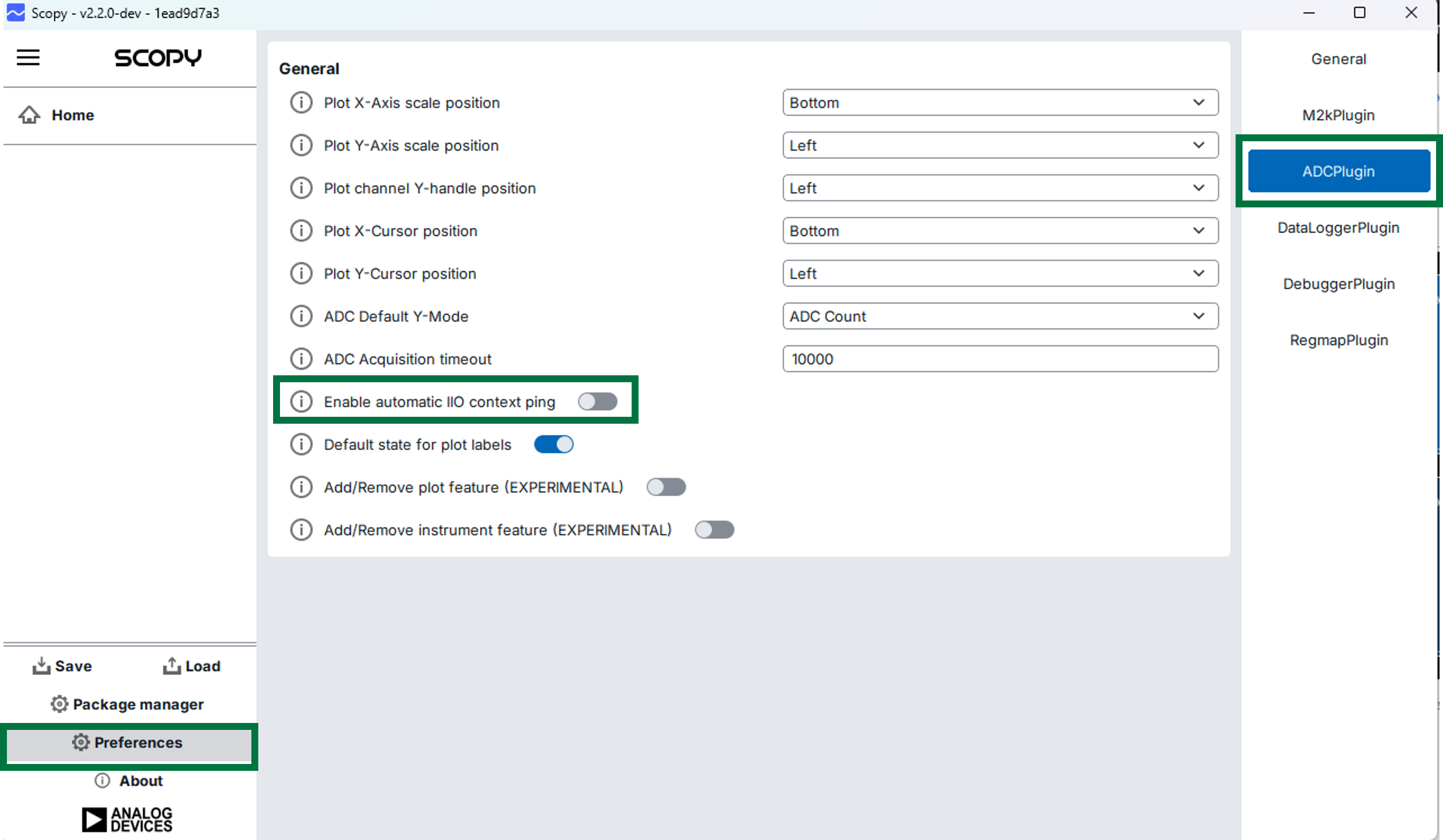
ADALM2000 Configuration
Open Scopy and navigate to Preferences, select ADCPlugin, and make sure that the Enable automatic IIO context ping option is disabled, as shown in the image below:
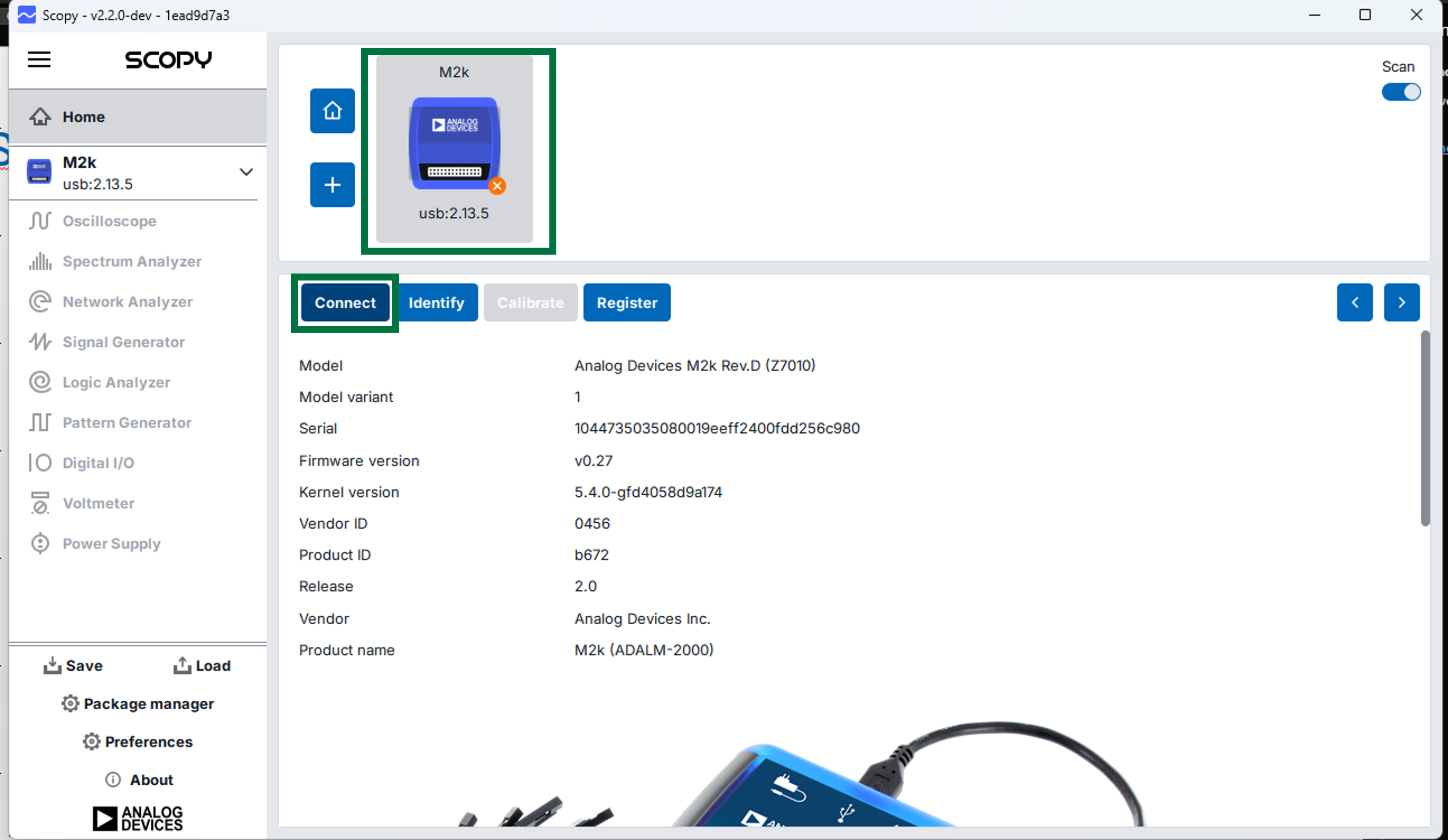
Plug in the USB cable and and connect to the M2K using Scopy, as presented in the figure below:
After successfully connecting to the M2K, configure the power supplies by setting the positive output to 5 V and the negative output to -2.5 V:
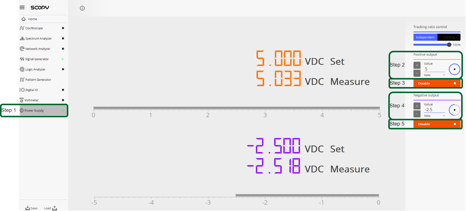
Figure 32 ADALM2000 power supply settings: Configure positive and negative supplies for converter operation (typically +5V and -2.5V).
Lastly, configure the signal generator to output a sinewave with 3 V amplitude, offset 2 V, 1 kHz frequency, and 0 deg phase on channel one, and a sinewave with the same parameters and a 180 deg phase on the second channel:
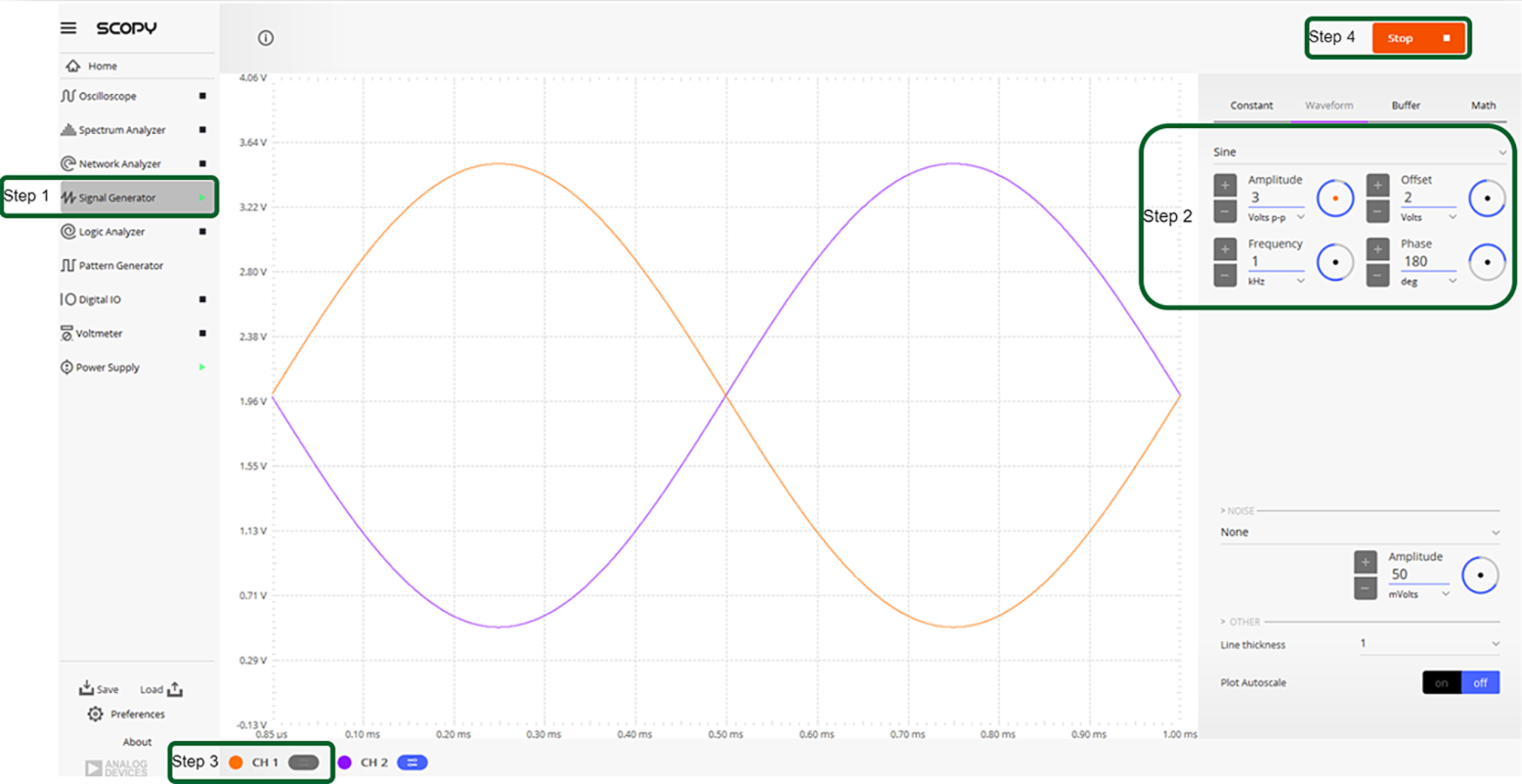
Figure 33 Function generator configuration: 1 kHz sine wave at -0.5 dBFS amplitude for SNR and THD testing.
UART Configuration
Verify the COM port assigned to the Cora development board and connnect to it via serial, using PuTTY (or similar a tool), as shown in the image below:
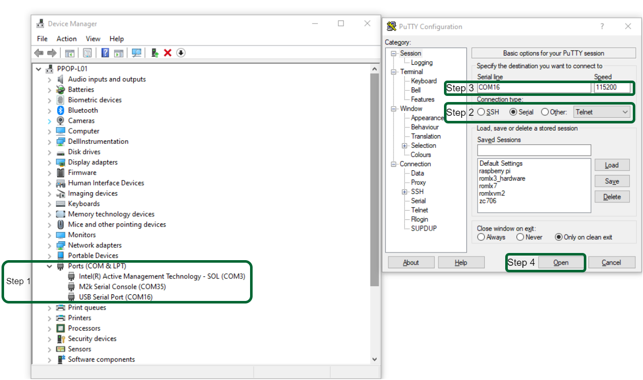
Figure 34 Serial terminal (PuTTY) configuration for board console access: 115200 baud, 8N1, no flow control.
Note
The ls -al /dev/serial/by-id command can be used to check serial ports on Linux.
Network Configuration
Important
Connecting the Cora development board to the internet is required in order to complete this workshop.
The IP address assigned to the Cora development board can be obtained by opening a terminal window using PuTTY and running the ifconfig command, as shown below. The IP address is shown as inet, under the eth0 interface.
~$
ifconfig
eth0: flags=4163<UP,BROADCAST,RUNNING,MULTICAST> mtu 1500
  inet 169.254.92.202  netmask 255.255.255.0  broadcast 10.48.65.255
  inet6 fe80::241:8f:d3d0:e43b  prefixlen 64  scopeid 0x20<link>
  ether 0e:23:90:e3:61:01  txqueuelen 1000  (Ethernet)
  RX packets 483757  bytes 81480222 (77.7 MiB)
  RX errors 0  dropped 0  overruns 0  frame 0
  TX packets 5562  bytes 775511 (757.3 KiB)
  TX errors 0  dropped 0 overruns 0  carrier 0  collisions 0
  device interrupt 38
lo: flags=73<UP,LOOPBACK,RUNNING> mtu 65536
  inet 127.0.0.1  netmask 255.0.0.0
  inet6 ::1  prefixlen 128  scopeid 0x10<host>
  loop  txqueuelen 1000  (Local Loopback)
  RX packets 83  bytes 10176 (9.9 KiB)
  RX errors 0  dropped 0  overruns 0  frame 0
  TX packets 83  bytes 10176 (9.9 KiB)
  TX errors 0  dropped 0 overruns 0  carrier 0  collisions 0
To check if the development board is reachable via LAN, you can use the ping command from a terminal or command prompt window, using the previously obtained IP address, as shown below:
~$
ping 169.254.92.202
Pinging 169.254.92.202 with 32 bytes of data:
Reply from 169.254.92.202: bytes=32 time=2ms TTL=64
Reply from 169.254.92.202: bytes=32 time=1ms TTL=64
Reply from 169.254.92.202: bytes=32 time=1ms TTL=64
Reply from 169.254.92.202: bytes=32 time=1ms TTL=64
Ping statistics for 169.254.92.202:
Packets: Sent = 4, Received = 4, Lost = 0 (0% loss),
Approximate round trip times in milli-seconds:
Minimum = 1ms, Maximum = 2ms, Average = 1ms
Evaluate System
Environment Setup
Setup the pyadi-iio Repository
First, connect to the Cora development board using PuTTY and create a workspace directory:
cd /media
mkdir workshop
cd workshop/
Clone the pyadi-iio repository and switch to the ad7984_demo branch:
git clone https://github.com/analogdevicesinc/pyadi-iio.git
cd pyadi-iio
git checkout ad7984_demo
After switching to the ad7984_demo branch, run the following command to install the required Python packages:
pip install .
Regular SPI Trigger Configuration
Navigate to the workspace and create a bash script for configuring the regular SPI trigger:
cd /media/workshop
touch tmr_conf_script.sh
chmod +x tmr_conf_script.sh
After creating the script, open it with a text editor and paste the following code:
#!/bin/bash
echo Setting the sampling rate to $1
cd /
mkdir -p configfs
if ! mountpoint configfs
then
   mount -t configfs none configfs
fi
mkdir -p configfs/iio/triggers/hrtimer/tmr0
cat /sys/bus/iio/devices/trigger0/name
cd /sys/bus/iio/devices
echo tmr0 > iio\:device0/trigger/current_trigger
echo 2048 > iio\:device0/buffer/length
echo $1 > trigger0/sampling_frequency
echo 1 > iio\:device0/scan_elements/in_voltage0-voltage1_en
echo 1 > iio\:device0/buffer/enable
Run the script with the sampling rate as a parameter:
/media/workshop$
./tmr_conf_script.sh 10000
Setting the sampling rate to 10000
configfs is not a mountpoint
tmr0
System Evaluation - Regular SPI Controller
Data Capture using Scopy
Note
Board IP Address: The Cora Z7S board IP address is 169.254.92.202
(previously obtained from running ifconfig command in PuTTY terminal)
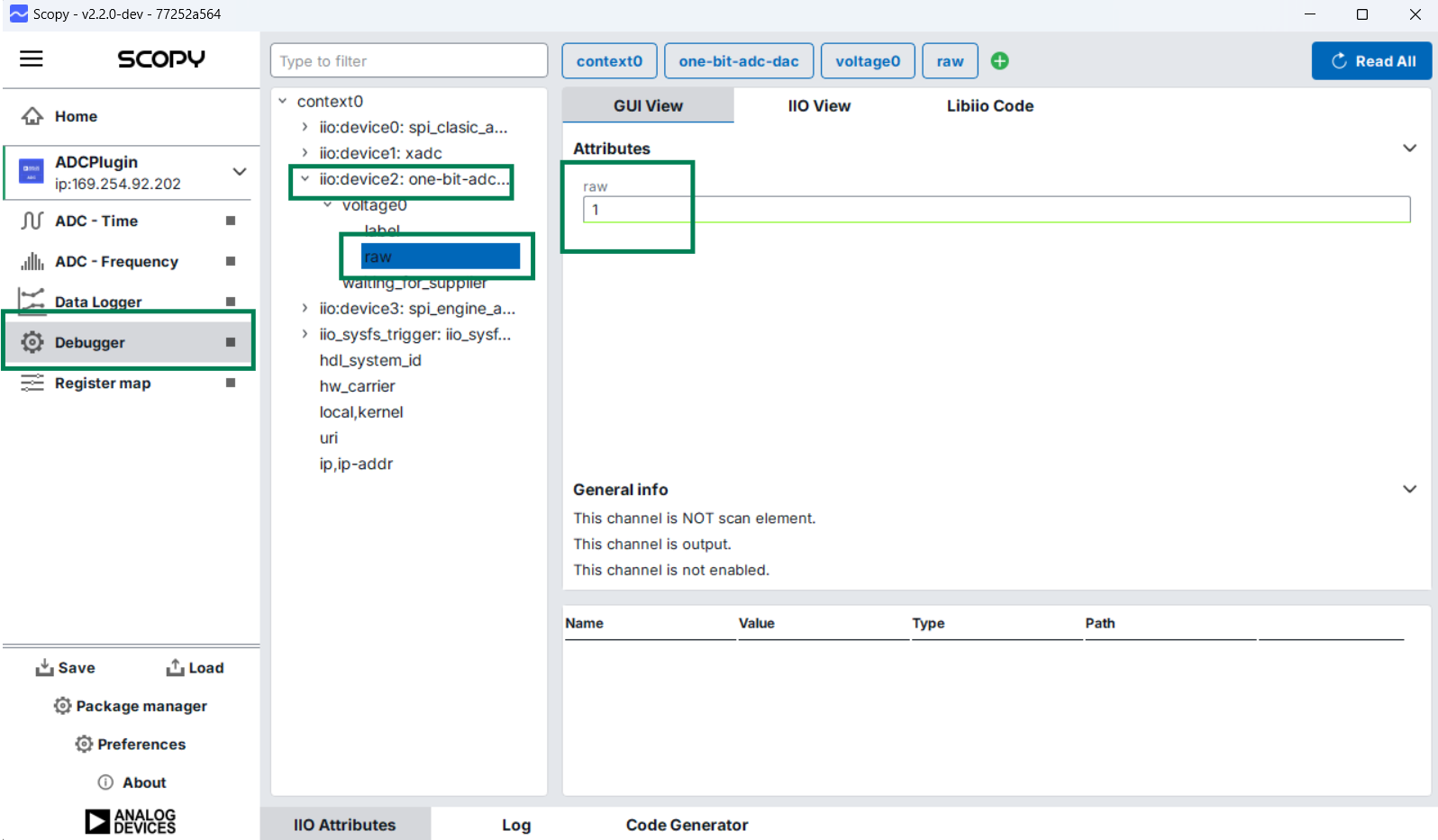
Scopy can be used to remotely connect to the Cora development board and display the data obtained from the ADC. To achieve this, go to the Home section in Scopy and add the device using the IP address of the development board, as shown below:
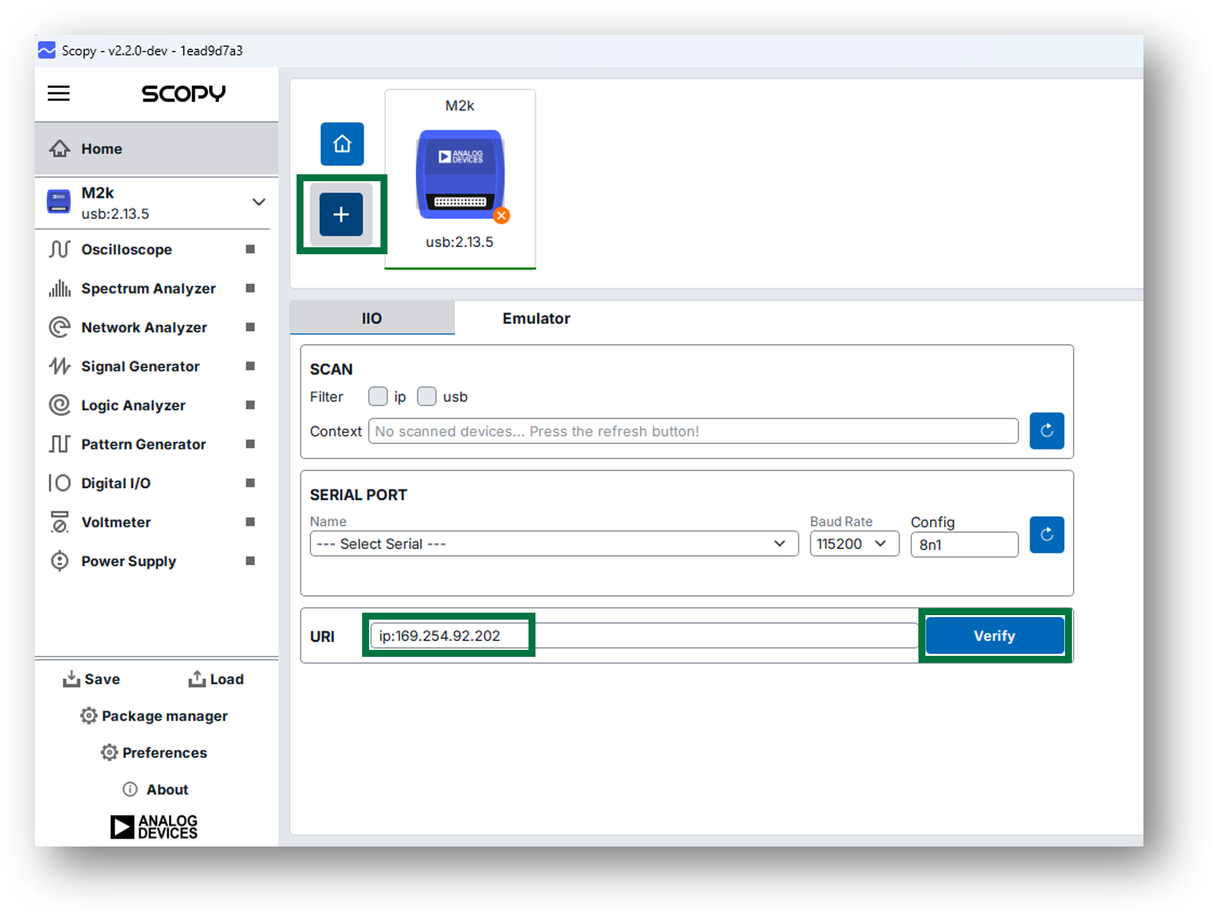
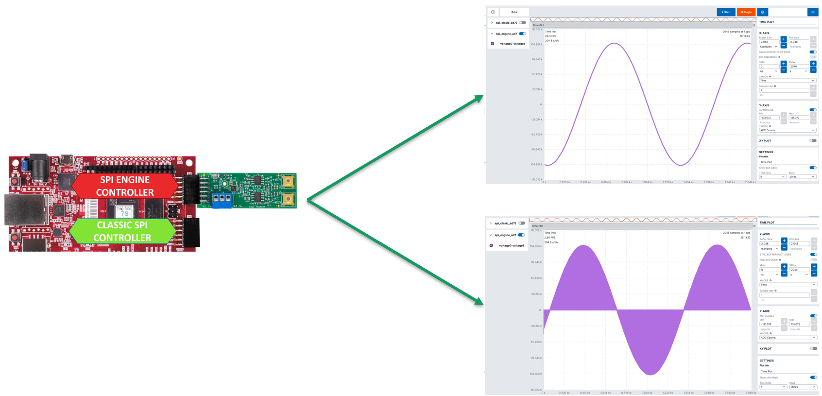
After the device was found, click on Add Device and then Connect. Your device should appear as ADCPlugin in the list on the left side of the window, next to the M2K. Open the ADC-Time section, select the spi_clasic_ad7984 channel and you should see the data obtained using the regular SPI transfers when you initialize a capture on the oscilloscope:
Data Capture using Python
To evaluate the performance of the SPI transfers, the ad7984_example.py Python script is provided:
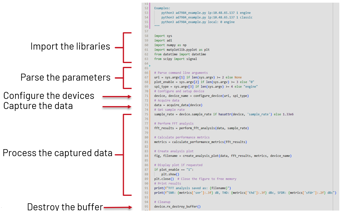
Navigate to the workshop folder and run the script with the following parameters:
~$
cd /media/workshop/
/media/workshop$
python pyadi-iio/examples/ad7984_example.py local: 0 classic
WARNING: High-speed mode not enabled
Raw data saved to: spi_clasic_ad7984_captured_data.txt
Using sample rate: 10000.0 Hz for classic mode
FFT analysis saved as: spi_clasic_ad7984_fft_analysis.jpg
SNR: 39.615 dB, THD: -53.204 dBc, SFDR: 39.62 dBc
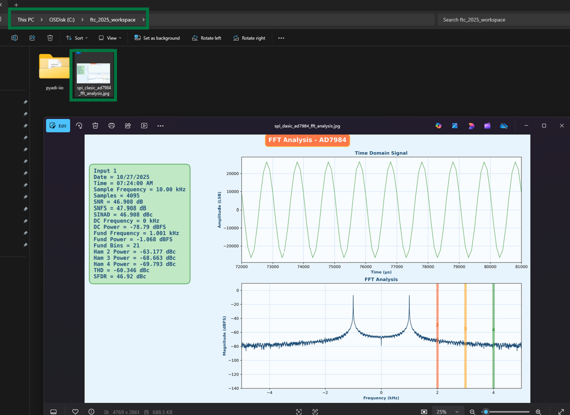
The result of the Python script is a FFT analysis of the input signal, saved as spi_clasic_ad7984_fft_analysis.jpg in the present directory. To create a copy of the resulted image, use the following command in a terminal window on your local machine, and, when prompted for the password, type analog:
scp root@169.254.92.202:/media/workshop/spi_clasic_ad7984_fft_analysis.jpg spi_clasic_ad7984_fft_analysis.jpg
Important
Make sure that the IP address and the path to the .jpg file match your setup.
The scp command creates a copy of the .jpg file on the present working directory of your local machine, and it should look like the following image:
Adittionaly, the Python script can also be executed from the local machine, using the IP of the Cora development board:
~/spi_workshop$
python pyadi-iio/examples/ad7984_example.py ip:169.254.92.202 1 classic
WARNING: High-speed mode not enabled
Raw data saved to: spi_clasic_ad7984_captured_data.txt
Using sample rate: 10000.0 Hz for classic mode
FFT analysis saved as: spi_clasic_ad7984_fft_analysis.jpg
SNR: 39.615 dB, THD: -53.204 dBc, SFDR: 39.62 dBc
Important
The pyadi-iio repository needs to be set up on the local machine, using the same steps presented before. Make sure that the IP address and the paths match your setup.
System Evaluation - SPI Engine
Data Capture using Scopy
To visualize the data obtained using the SPI engine, move the EVAL-AD7984-PMDZ to the JA PMOD connector and select the spi_engine_ad7984 channel in ADC-Time section, as shown in the image below:
Data Capture using Python
To evaluate the performance of the SPI engine, run the ad7984_example.py script with the following parameters:
/media/workshop$
python pyadi-iio/examples/ad7984_example.py local: 0 engine
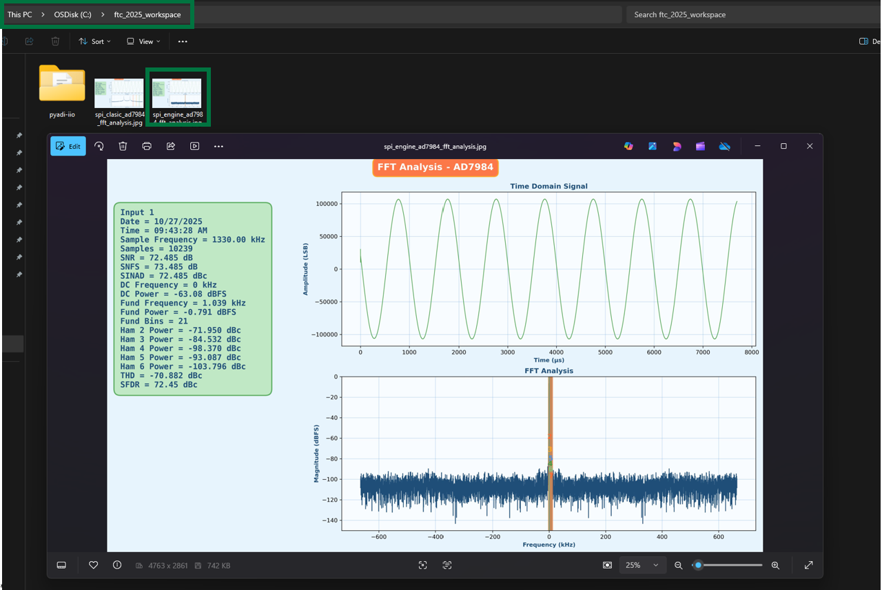
Raw data saved to: spi_engine_ad7984_captured_data.txt
Using sample rate: 1330000.0 Hz for engine mode
FFT analysis saved as: spi_engine_ad7984_fft_analysis.jpg
SNR: 70.394 dB, THD: -66.987 dBc, SFDR: 70.37 dBc
Use the following command, with analog as password, to create a copy of spi_engine_ad7984_fft_analysis.jpg on your local machine:
scp root@169.254.92.202:/media/workshop/spi_engine_ad7984_fft_analysis.jpg spi_engine_ad7984_fft_analysis.jpg
Important
Make sure that the IP address and the path to the .jpg file match your setup.
The results obtained should resamble the image below:
Similar to the previous case, the Python script can be executed from the local machine, for the SPI engine scenario, as shown below:
~/spi_workshop$
python pyadi-iio/examples/ad7984_example.py ip:169.254.92.202 1 engine
Raw data saved to: spi_engine_ad7984_captured_data.txt
Using sample rate: 1330000.0 Hz for engine mode
FFT analysis saved as: spi_engine_ad7984_fft_analysis.jpg
SNR: 70.394 dB, THD: -66.987 dBc, SFDR: 70.37 dBc
Important
The pyadi-iio repository needs to be set up on the local machine, using the same steps presented before. Make sure that the IP address and the paths match your setup.
Performance Results Comparison
Note
SPI Engine Achieves Near-Datasheet Performance
Regular MCU SPI controllers achieve only 15% of datasheet SNR, while SPI Engine delivers 79% even at low sample rates and 100% of THD at maximum rate.
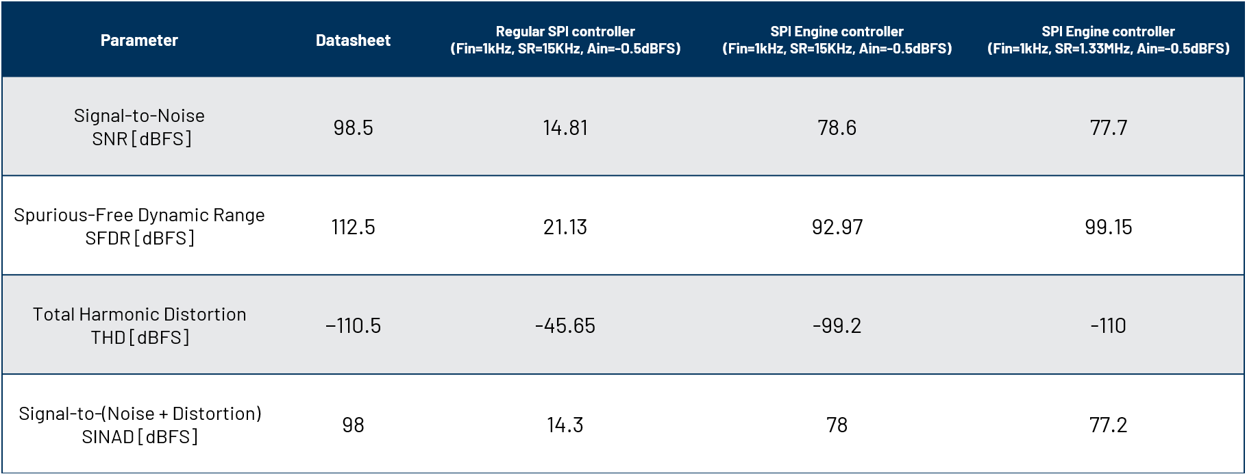
Figure 41 Performance comparison between the regular SPI controller and SPI engine.
Performance Analysis:
Metric |
Regular SPI |
SPI Engine |
|---|---|---|
SNR Achievement |
15% of datasheet |
79-89% of datasheet |
Sample Rate |
15 KSPS (1.1%) |
1.33 MSPS (100%) |
CPU Usage |
High (100% per transfer) |
Minimal (<1%) |
Timing Jitter |
Variable (μs range) |
Deterministic (<1 ns) |
Key Takeaway
The SPI Engine framework enables precision converters to achieve their full datasheet specifications by providing deterministic, low-jitter timing that traditional MCU SPI controllers cannot deliver.
Audio Signal Quality Comparison
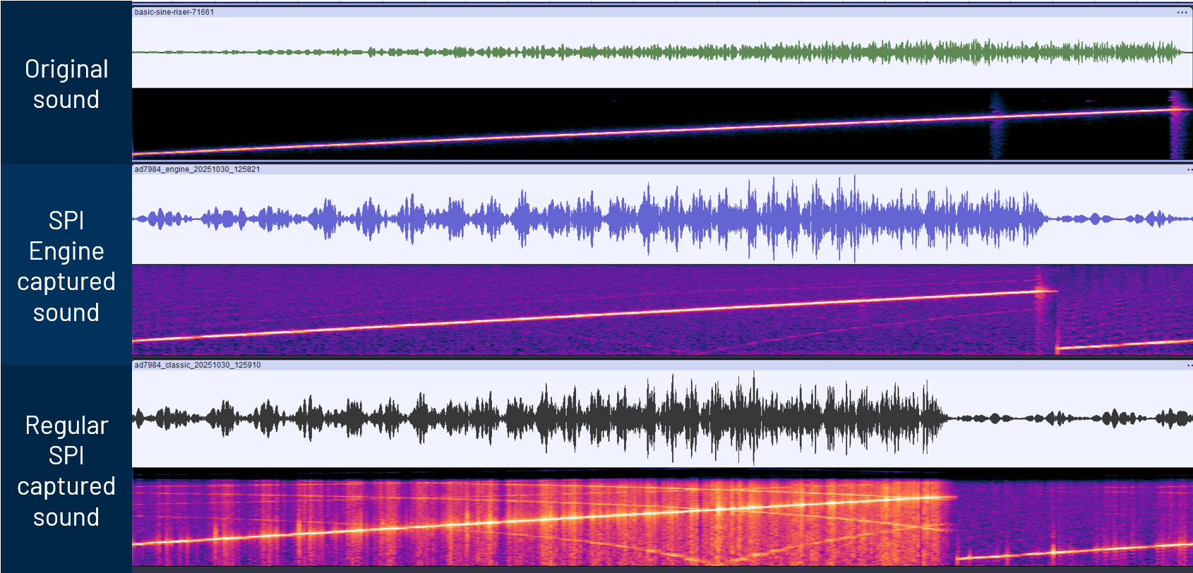
Figure 42 Audio quality comparison: Regular SPI controller (left) shows distorted waveform with visible noise and jitter artifacts, while SPI Engine (right) delivers clean, high-fidelity signal reproduction with minimal distortion.
Debug Options - Logic Analyzer from Scopy
The M2K is used to probe the SPI signals on pins IO0-IO3 on the Cora Z7S development board. To visualize the signals, open the Logic Analyzer in Scopy and cofigure it as shown in the images below:
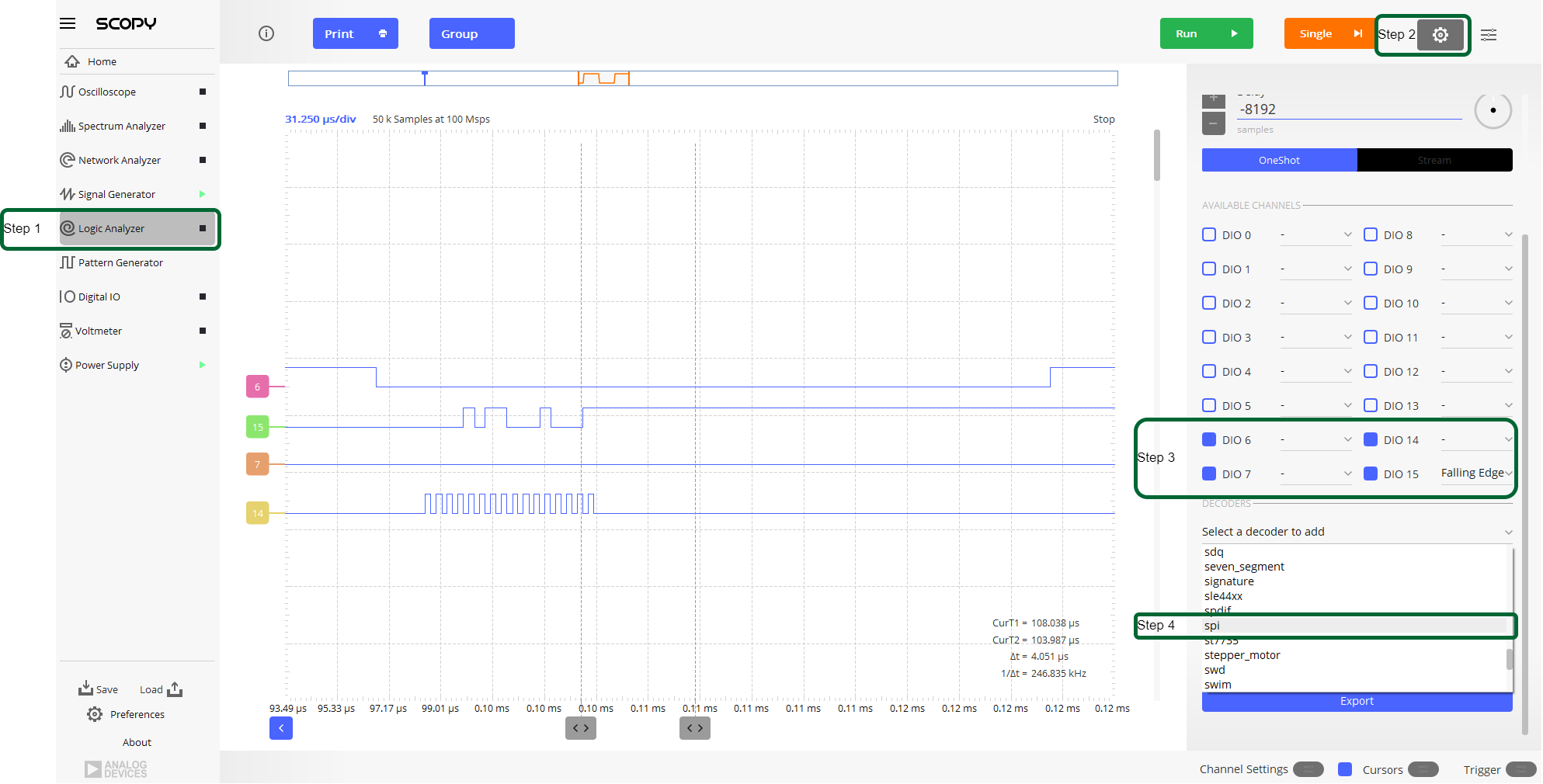
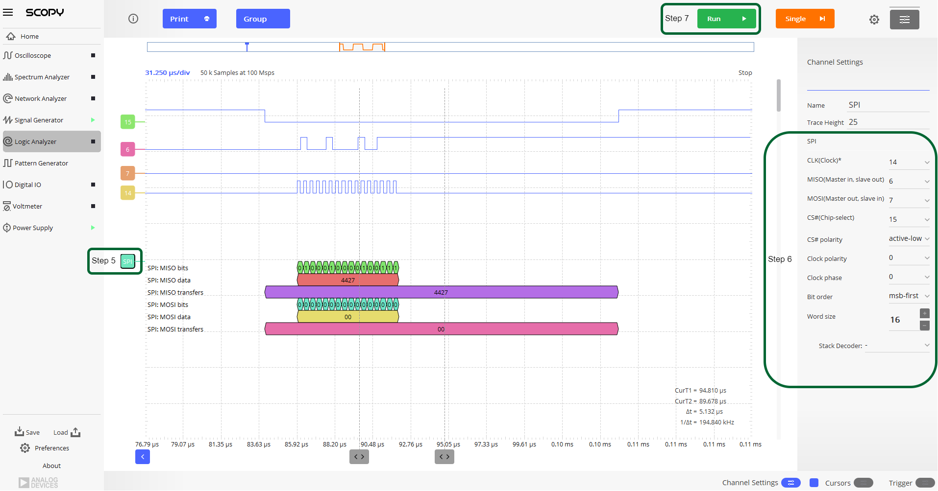
By default, the signals on pins IO0-IO3 correspond to the regular SPI scenario. To see the signals for the SPI engine scenario, you need to change the value of GPIO[34] to 1, following the steps in the figure below:
Important
To visualize the SPI signals for the SPI engine scenario, a higher bandwidth oscilloscope must be used.
Debug Options – Integrated Logic Analyzer (ILA)
For further debuging options, two ILA instances have been added to the design as shown in the diagram below:
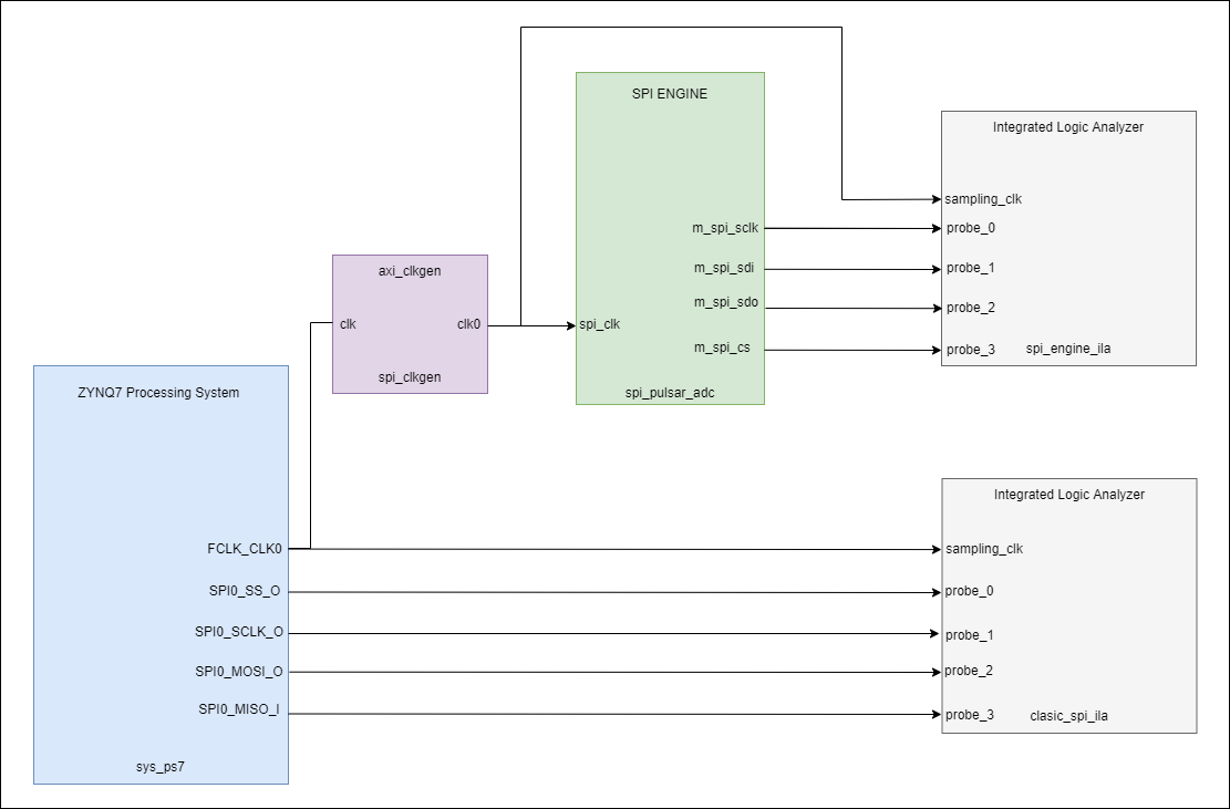
Figure 46 Xilinx ILA configuration for capturing SPI Engine signals and debugging timing issues.
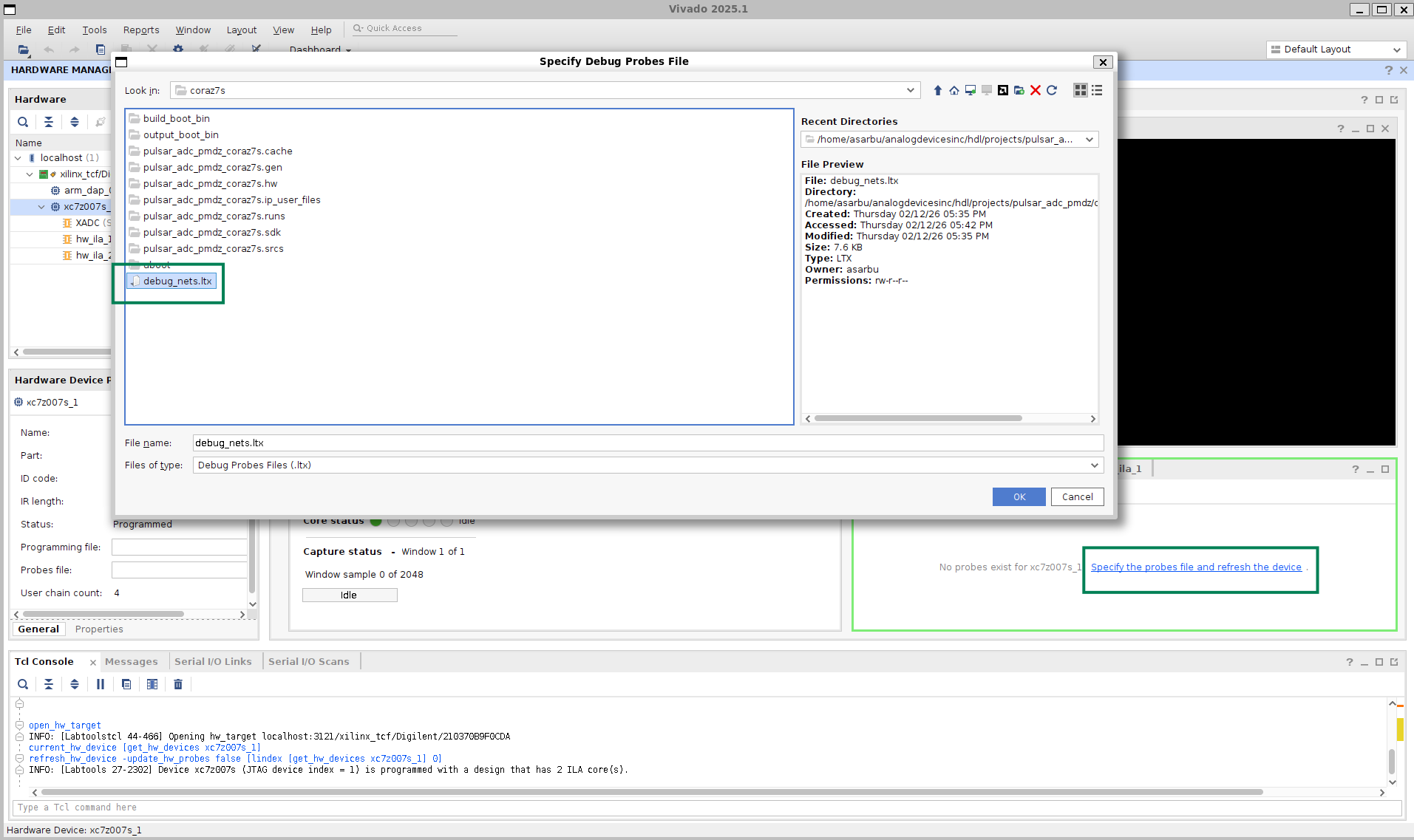
To use the ILA, open the Hardware Manage in Vivado and connect to the Cora development board. After you successfully connected to the target, configure the probes by clicking on Specify the probes file and refresh the device, navigating to ~/spi_workshop/hdl/projects/pulsar_adc_pmdz/coraz7s, selecting debug_nets.ltx, and refreshing the device, as shown below:
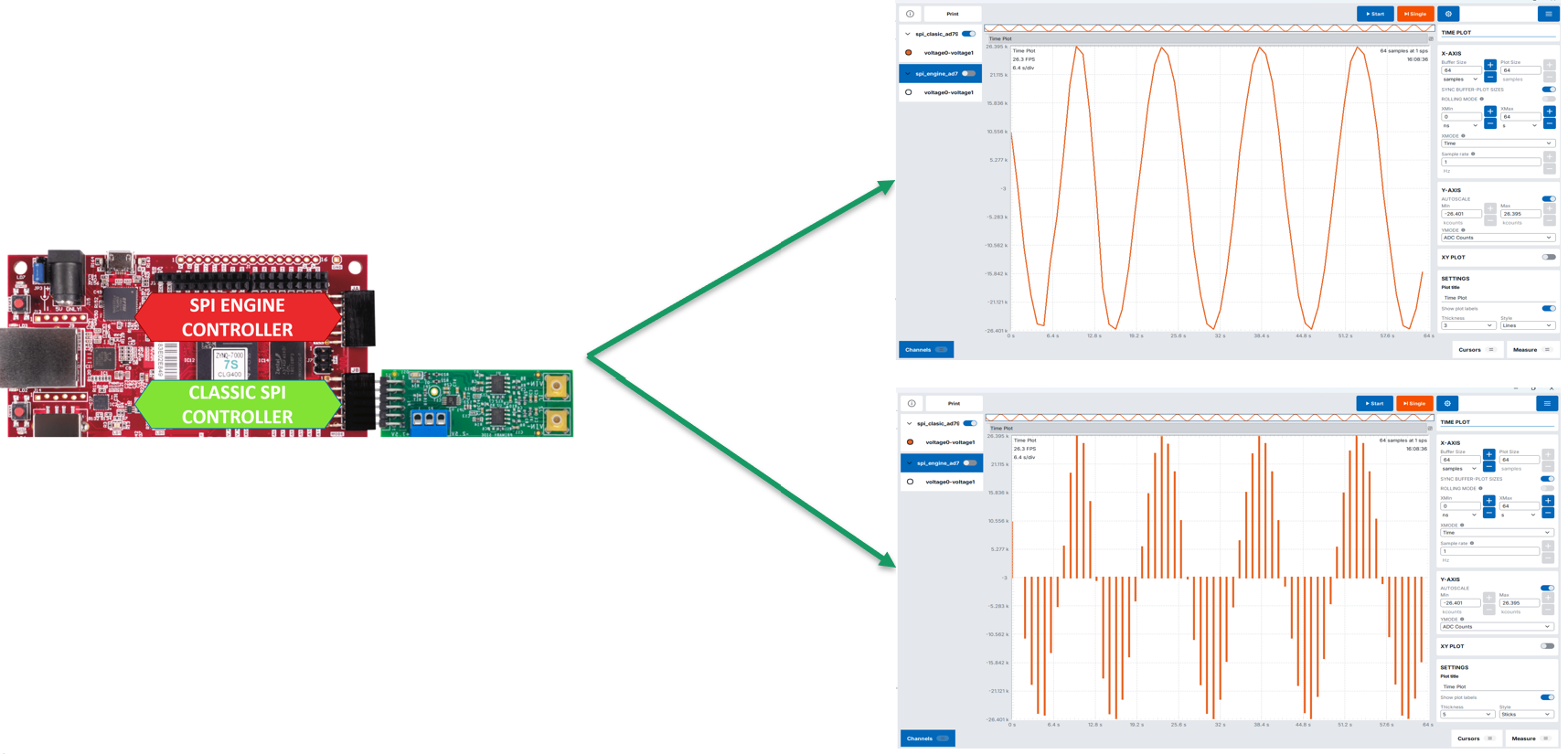
Comparison: Regular SPI vs. SPI Engine Waveforms
After successfully configuring the probes, hw_ila_1 and hw_ila_2 can be used to visualize the SPI signals for the regular and engine use cases. The images below show the comparison between the two cases, using ILA:
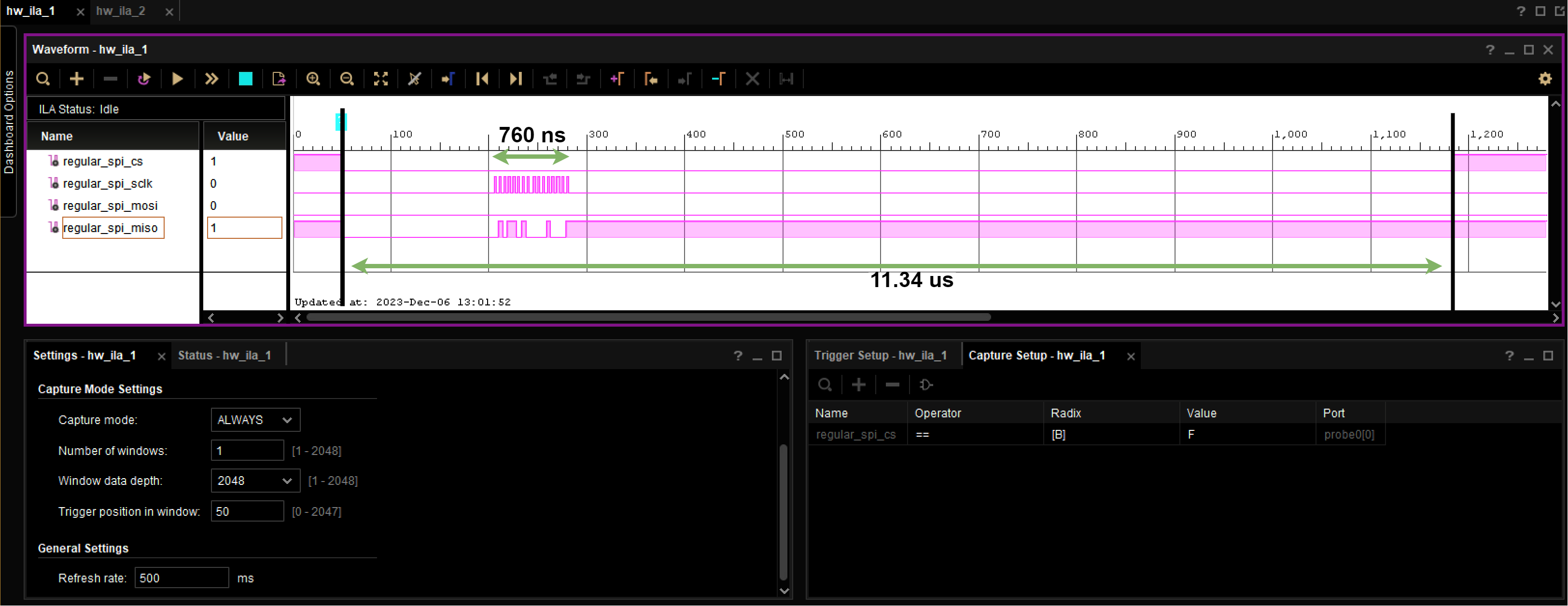
Figure 48 Regular SPI Controller: Irregular timing, software-induced delays, visible jitter between conversions.
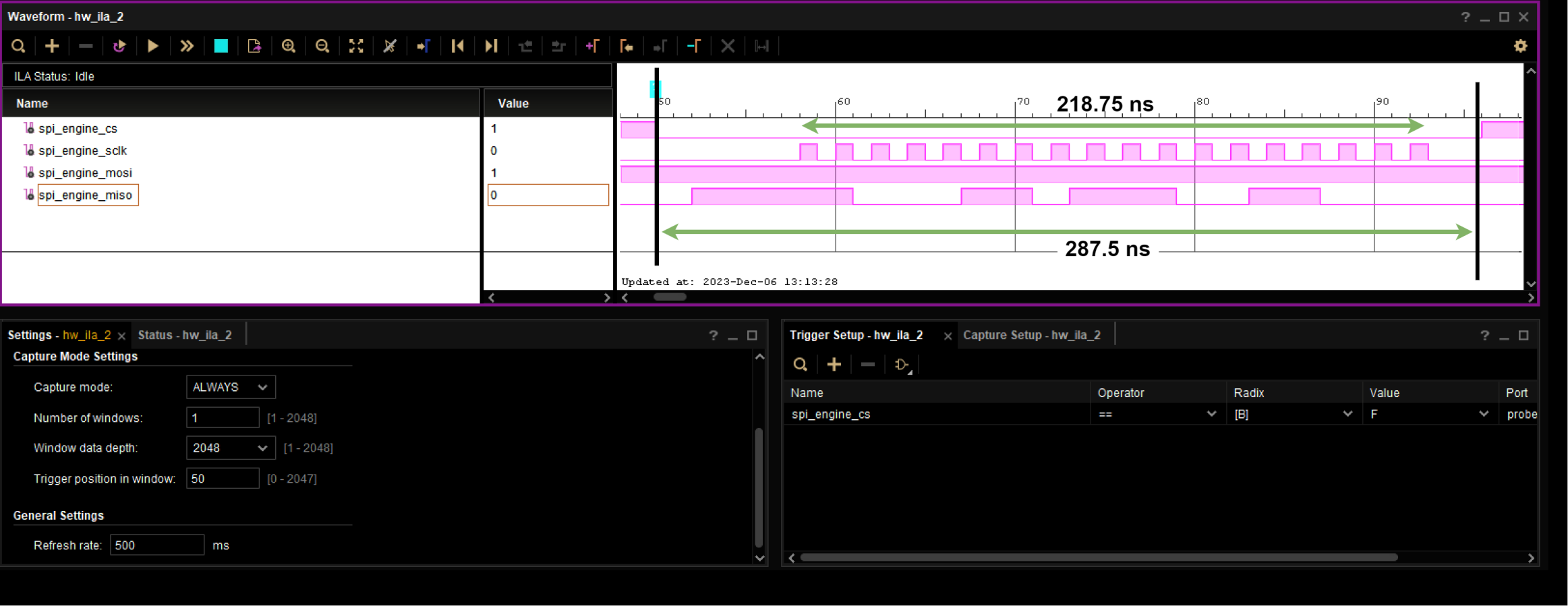
Figure 49 SPI Engine Controller: Precise timing, consistent conversion intervals, deterministic operation at full 1.33 MSPS rate.
Conclusions
Workshop Summary
Through this hands-on workshop, we demonstrated the dramatic performance improvement achievable with FPGA-based SPI Engine compared to traditional MCU SPI controllers.
Key Findings:
MCU SPI Limitations: Traditional MCU controllers are suitable only for converters with sampling rates up to ~100 KSPS and can achieve only 15-20% of a converter’s datasheet performance.
FPGA Requirement for Maximum Performance: Achieving full datasheet specifications (sampling rate, SNR, THD) requires FPGA-based timing control with deterministic, low-jitter operation.
SPI Engine Framework: This highly flexible, open-source SPI controller framework successfully interfaces with a wide range of precision converters, providing:
Hardware-driven, deterministic timing
Support for 1+ MSPS continuous streaming
Near-datasheet AC performance (>79% SNR achievement)
Minimal CPU overhead (<1%)
Production-Ready Solution Stack: The complete open-source ecosystem provides HDL, Linux drivers, and tools for rapid development and deployment.
Performance Achieved:
1.33 MSPS continuous sampling (vs. 15 KSPS with MCU SPI)
77.7 dB SNR at full rate (vs. 14.8 dB with MCU SPI)
-110 dB THD matching datasheet (vs. -45.6 dB with MCU SPI)
Thank You!
Related Workshops and Presentations:
My customer uses an FPGA in his product. Now what?
ADALM2000 in real life applications
Just enough Software and HDL for High-Speed designs
Hardware and Software Tools for Precision Wideband Instrumentation
Questions? Community Support:
For technical questions and community discussions: