EVAL-CN0584-EBZ
Precision Low Latency Development Kit.
Overview
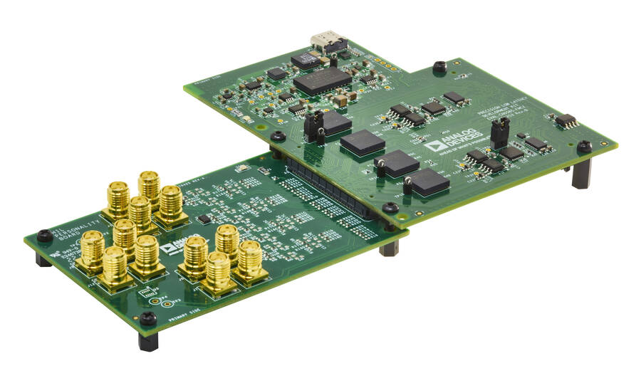
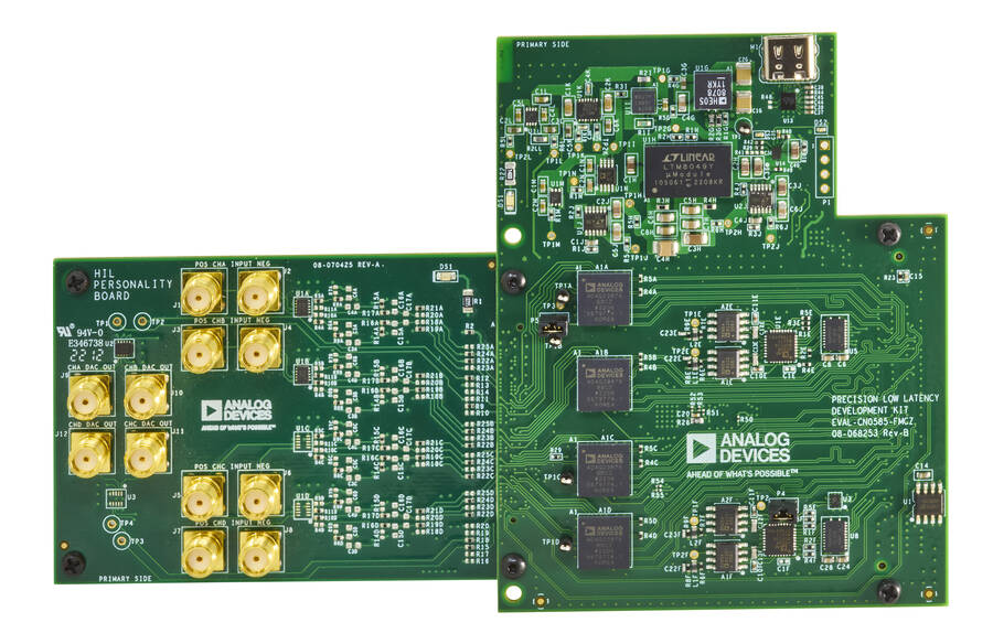
The CN0584 Low Latency Development Kit is a development platform consisting of two boards the EVAL-CN0585-FMCZ and the EVAL-CN0584-EBZ.
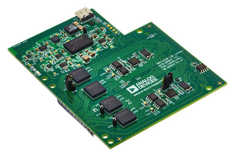
EVAL-CN0585-FMCZ consists of 4 x 16-bit ADC channels and 4 x 16-bit DAC channels that are interfaced with an FPGA through the FMC Low Pin Count (LPC) Connector. Current revision of EVAL-CN0585-FMCZ is Rev B. EVAL-CN0584-EBZ is the application specific analog front end (AFE) board. CN0584 is connected to a Zedboard to build a development system setup.
The Low Latency Development Kit (LLDK) provides a complete data acquisition and signal generation platform with on-board power rails, voltage monitoring, logic level translation, general purpose I/O, I2C, SPI, and a personality interface connector.
The key performance benefit of the LLDK system is the ability to perform a complete capture and conversion of precision analog input data in <70ns with the ADC module and generate a settled full-scale analog output in <200ns from initial data written to the DAC.
Connections and Configurations

ADC Inputs
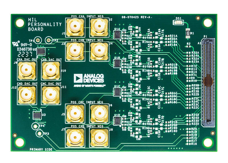
There are four channels of differential input signals on EVAL-CN0584-EBZ.
Channel |
Positive Input Signal |
Negative Input Signal |
|---|---|---|
Channel 0 |
J1 |
J2 |
Channel 1 |
J3 |
J4 |
Channel 2 |
J5 |
J6 |
Channel 3 |
J7 |
J8 |
ADC Input Range Configuration
This LLDK has configurable input voltage ranges of ±10V (Default), ±5V, ±4.096V, ±2.5V, and ±1.5V. The input range can be changed by modifying resistor placements on EVAL-CN0584-EBZ as described in Table 2.
DAC Outputs
LLDK can support multiple output voltage ranges which can be configured, such as 0V to 2.5V, 0V to 5V, −5V to +5V, and −10V to +10V, and custom intermediate ranges with full 16-bit resolution. In order to change the output range, resistor placements on the AFE board must be modified and register settings must be applied to AD3552R on EVAL-CN0585-FMCZ as described in Table 4.
Voltage Reference
The default ADC reference configuration uses the internal 2.048V, ±0.1% accurate, 20ppm/°C max voltage reference. For more stringent use cases where the accuracy and temperature drift is an issue, an external LTC6655 2.048V, ±0.025% accurate, 2ppm/°C max voltage reference can be used.
The default DAC reference configuration uses the internal 2.5V, ±0.3% accurate, 10ppm/°C max voltage reference. For more stringent use cases where the accuracy and temperature drift is an issue, an external ADR4525 2.5V, ±0.02% accurate, 2ppm/°C max voltage reference can be used.
Power Supply Considerations and Configuration
All power for CN0584 is provided by EVAL-CN0585-FMCZ through the analog front end (AFE) connector. CN0584 uses the +15V and -15V rails to provide the positive and negative supply voltages for the ADG5421F input protection switches. The +12V and -12V rails provide the positive and negative supply voltages for the ADA4898-1 ADC buffer amplifiers. The +3.3V rail powers the EEPROM circuit.
Power tree information can be found in EVAL-CN0585-FMCZ. Table 6 provides more details on LLDK power rails:
System Setup Using a ZedBoard
CN0584 is fully supported using a ZedBoard.
The following is a list of items needed for system setup:
Hardware
- EVAL-CN0585-FMCZ(RevB)
(Note: Figure 4 features EVAL-CN0585-FMCZ RevA board. Current LLDK system has RevB board shown in Figure 5, same connectors and functionalities, only different in USB-C power supply.)
ZedBoard Rev D or later board
12Vdc, 3A power supply
16GB (or larger) Class 10 (or faster) micro-SD card (included in the box)
USB-C power source (included in the EVAL-CN0585-FMCZ RevB box)
Micro-USB to Type-A cable
Ethernet cable
- User interface setup (choose one):
HDMI monitor, keyboard, and mouse plugged directly into the ZedBoard
Host Windows/Linux/Mac computer on the same network as the ZedBoard
Software
Host PC (Windows or Linux)
A UART terminal if need to access Linux system on the ZedBoard (Putty/TeraTerm/Minicom, etc.), Baud rate 115200 (8N1)
Loading Image on SD Card
The box includes a pre-programmed SD card. You can skip the steps in this section and go to the Setting up the Hardware if using the provided card.
To boot the ZedBoard and control the EVAL-CN0585-FMCZ, you will need to install ADI Kuiper Linux on an SD card. Complete instructions, including where to download the SD card image, how to write it to the SD card, and how to configure the system are provided on the Kuiper.
Configuring the SD Card
Follow the configuration procedure under Configuring the SD Card for FPGA Projects on Kuiper.
Copy the following files onto the boot directory to configure the SD card:
uImage file for Zynq
BOOT.BIN specific to your EVAL-CN0585-FMCZ + ZedBoard
setup_adc.sh file for setting up ADC
devicetree.dtb devicetree for Zynq specific to your EVAL-CN0585-FMCZ + ZedBoard.
The device tree describes the following devices:
one-bit-adc-dac– controls the MAX7301axi_pwm_gen– generates the CNV signal for analog-to-digital convertersref_clk– generates the sample clock for ADAQ23876 devices and the reference clock for AD3552R devicesrx_dma– controls the DMA for RX pathLtc2387– controls ADAQ23876 devicesqspi0– controls the SPI devices that are connected to the PL SPI IPdac0_tx_dma- controls the DMA for the first AD3552R devicedac1_tx_dma- controls the DMA for the second AD3552R deviceaxi_ad3552r_0– controls the first AD3552R deviceaxi_ad3552r_1– controls the second AD3552R deviceI2C– controls devices that are connected to PL I2C IP (eeprom, eeprom2, ad7291_1)
Setting up the Hardware
Prepare the ZedBoard.
Insert the SD card into the SD Card Interface Connector (J12).
Connect the EVAL-CN0585-FMCZ board into the ZedBoard FMC connector.
Connect the EVAL-CN0584-EBZ board into the EVAL-CN0585-FMCZ.
Connect micro USB to UART port (J14), and the other end to the host PC.
Connect the ethernet cable to RJ45 ethernet connector (J11), and the other end to the host PC.
Plug the Power Supply into the 12V Power ZedBoard input connector (J20). DO NOT turn the device on.
Plug USB-C power supply to EVAL-CN0585-FMCZ (revB only).
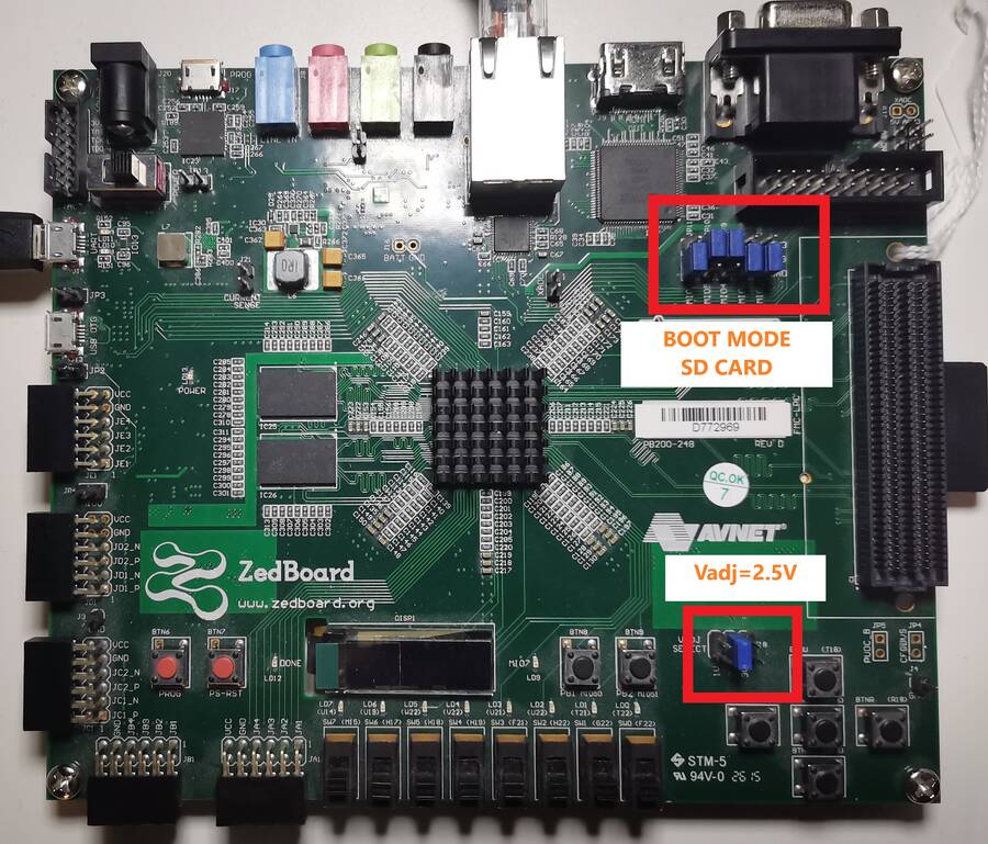
Set the jumpers as seen in figure below.
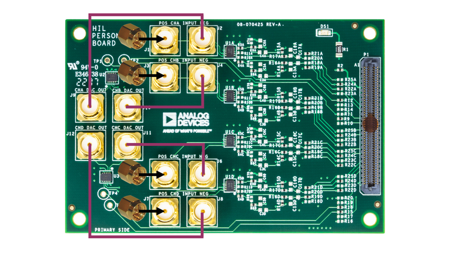
Connect the DAC output connectors to the negative ADC input connectors as shown in Figure 7 using coax cables (e.g., DAC0 to ADC0-neg, DAC1 to ADC1-neg, etc.). Terminate the positive ADC connectors with 50ohms SMA terminators.
Turn the ZedBoard on.

All the products described on this page include ESD (electrostatic discharge) sensitive devices. Electrostatic charges as high as 4000V readily accumulate on the human body or test equipment and can discharge without detection. Although the boards feature ESD protection circuitry, permanent damage may occur on devices subjected to high-energy electrostatic discharges. Therefore, proper ESD precautions are recommended to avoid performance degradation or loss of functionality. This includes removing static charge on external equipment, cables, or antennas before connecting to the device.
Application Software (both locally and remotely on the FPGA)
The CN0584 can be interfaced with using IIO Oscilloscope, Python, or MATLAB to enable device configuration, capture of incoming samples from the ADCs, and generation of waveforms to be transmitted by the DACs.
Hardware Connection
Libiio is a library used for interfacing with IIO devices and must be installed on your computer to interface with the hardware.
Download and install the latest Libiio package on your machine.
To connect to your device, the IIO Osciloscope software must be able to create a context. The context creation in the software depends on the backend used to connect to the device as well as the platform where the EVAL-CN0585-FMCZ is attached. The ZedBoard running ADI Kuiper Linux is currently the only platform supported for the CN0585.
The user needs to supply a Uniform Resource Identifier (URI) which will be used in the context creation. To get the URI, use the command iio_info in the terminal. The iio_info command is a part of the libIIO package that reports all IIO attributes. Upon installation, simply enter the command on the terminal command line to access it.
For FPGA (ZedBoard) Direct Local Access
iio_info
For Windows machine connected to an FPGA (ZedBoard)
iio_info -u ip:<ip address of your ip>
Example:
* If your ZedBoard has the IP address 169.254.92.202, you have to use //iio_info -u ip::169.254.92.202// as your URI
Note
Do note that the Windows machine and the FPGA board should be connected to the same network for the machine to detect the device.
IIO Oscilloscope
IIO Oscilloscope is a cross platform GUI application which can interface with different evaluation boards from within a Linux system.
Important
Make sure to download/update to the latest version of IIO Oscilloscope.
Once done with the installation or an update of the latest IIO Oscilloscope, open the application. The user needs to supply a URI which will be used in the context creation of the IIO Oscilloscope. If there’s only one platform is connected, the IIO Oscilloscope will find URI automatically; if more than one platforms are connected, the user needs to supply the specific URI. The instructions to obtain the URI can be found in the previous section.
Note: the “Serial Context” connection method is not enabled.
Press
Refreshto display available IIO Devices and pressConnect.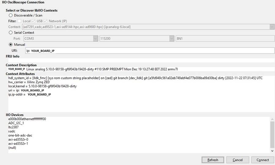
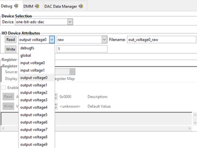
After the board is connected, select the one-bit-adc-dac-device, which is the controller for the MAX7301ATL+ I/O Expander. Then, configure pins values of output voltages 0 through 9, by setting the raw value to 1.
Press Write to confirm.
Input sources for AD3552R devices axi-ad3552r-0 and axi-ad3552r-1 can be configured as dma_input, ramp_input, or adc_input.
dma_input: DAC input is driven by signals generated by Matlab stored in DMA.
ramp_input: DAC input is driven by ramp signal generated by Matlab stored in DMA.
adc_input: For passthrough models, DAC input is driven by ADC output. For models with integrated HDL_DUT, DAC input is driven by HDL_DUT outputs.
Select the desired input source for both AD3552R devices axi-ad3552r-0 and axi-ad3552r-1 as dma_input.
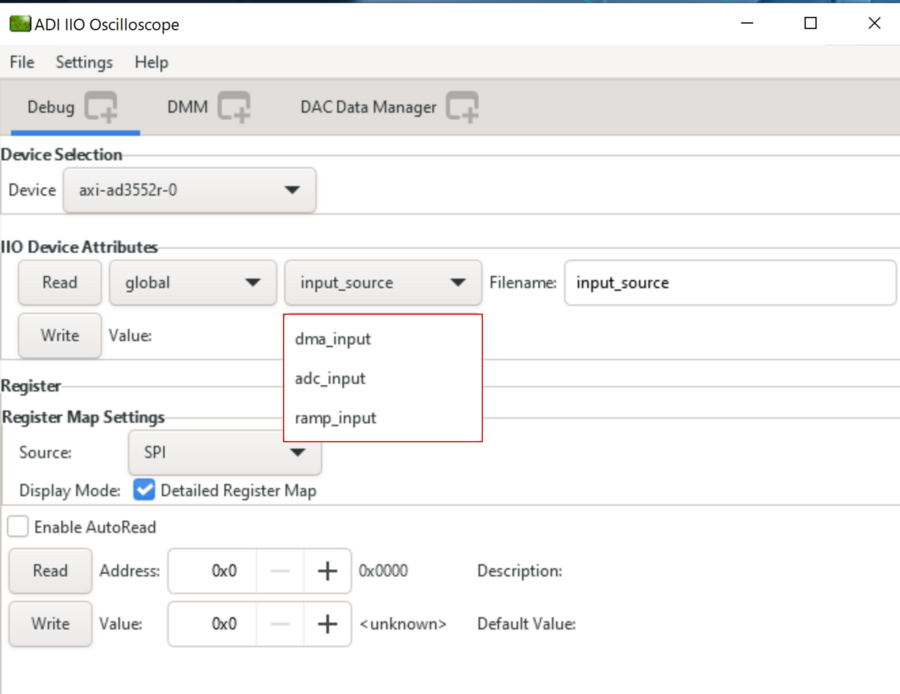
Figure 11 AD3552R Input Source Selection in IIO Oscilloscope
Important
Even if the input source is set to adc_input or ramp_input the steps regarding the DAC Data Manager tab have to be followed.
Select the desired output range for both AD3552R devices.
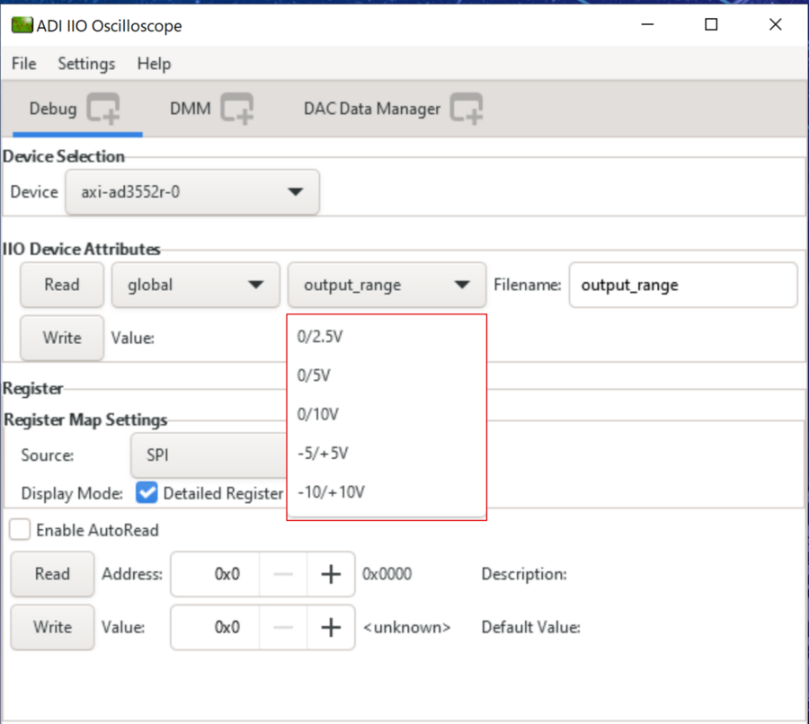
Figure 12 AD3552R Output Range Selection in IIO Oscilloscope
Warning
Make sure you don’t try to read/write the output_range attribute when the stream_status is in start_stream or start_stream_synced.
Important
After changing the output range, the board should be power cycled to ensure the DACs operate properly.
From the DAC Data Manager Window select the output channels of the DAC and enable the cyclic buffer for each DAC.
Load an example file (.mat, .txt, etc) from the IIO Oscilloscope installation directory, under Program Files/IIO Oscilloscope/lib/osc/waveforms folder.
Important
If the source is set as dma_input and the data from all 4 channels needs to be synchronized, make sure that you press the load button for the axi-ad3552r-1 device first then for axi-ad3552r-0.
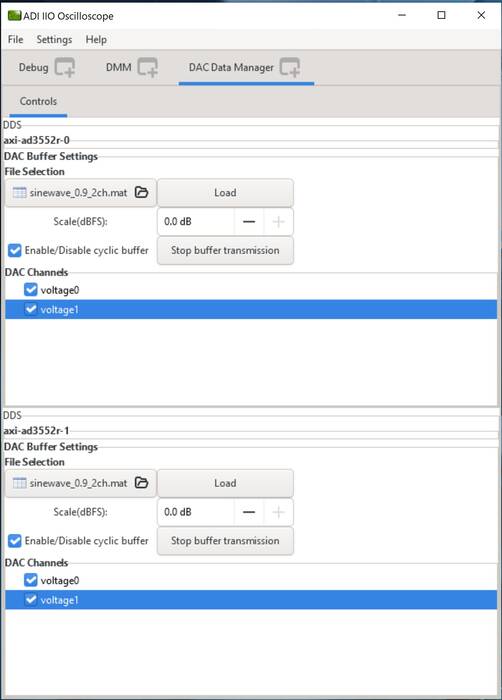
Click on the
Loadbutton.From the Debug window, select the stream_status IIO Attribute and start the stream (start_stream_synced means that all 4 channels are updated at the same time and the data streaming process waits for both DACs to be started).
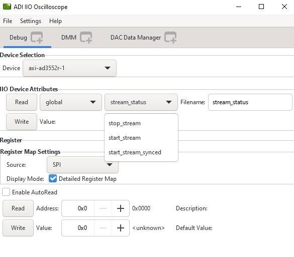
After the stream_status has been written and 4 channels are enabled, hit play button. Then data capture window can be seen like in Figure 15.
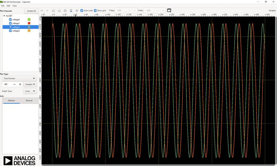
Important
Note that there is a phase delay between voltage0/voltage2 and voltage1/voltage3 because the DAC device channels are updated consecutively. See the DAC UPDATE MODES section of the AD3552R Data Sheet.
Warning
If you intend to stop the stream transmission and start it again synchronized, set the stream_status IIO Attribute to stop_stream for axi-ad3552r-1 device first then for the axi-ad3552r-0 device.
PyADI-IIO
The CN0584 can be interfaced to Python using the PyADI-IIO. PyADI-IIO is a Python abstraction module to simplify interaction with IIO drivers on ADI hardware. This module provides device-specific APIs built on top of the current libIIO Python bindings. These interfaces try to match the driver naming as much as possible without the need to understand the complexities of libIIO and IIO.
Follow the step-by-step procedure on how to install, configure, and set up PyADI-IIO and install the necessary packages/modules needed by referring to PyADI-IIO.
Running the example
Download
Github link for the Python sample script: CN0585 Python Example
Download or git clone pyadi-iio repository to your local drive.
If direct downloading ZIP folder, make sure to download from cn0585_v1 branch.
If cloning the repository using Git, type
git checkout cn0585_v1to switch to the correct branch.
Install additional packages.
pip install tk pytest paramiko matplotlib
Do above in the command prompt window. In general, use pip install “package name” to install any missing package.
After installing and configuring PYADI-IIO on your machine, you are now ready to run Python script examples. To follow this example, navigate to pyadi-iio folder (For example, “D:\pyadi-iio” is where pyadi-iio folder is located). Then run the cn0585_fmcz_example.py found in the examples folder.
D:\pyadi-iio>set PYTHONPATH=D:/pyadi-iio/
D:\pyadi-iio>python examples/cn0585_fmcz_example.py ip:your_board_ip
Press enter and lines below will be observed:
$ python examples/cn0585_fmcz_example.py
uri: ip:your_board_ip
############# EEPROM INFORMATION ############
read 256 bytes from /sys/devices/soc0/fpga-axi@0/41620000.i2c/i2c-1/1-0050/eeprom
Date of Man     : Fri Jan 20 08:11:00 2023
Manufacturer    : Analog Devices
Product Name    : LLDK-LTC2387-AD3552R
Serial Number   : 56864654
Part Number     : 1234
FRU File ID     : 12131321
PCB Rev         : VB
PCB ID          : HIL
BOM Rev         : VC
Uses LVDS       : Y

#############################################
GPIO4_VIO state is: 0
GPIO5_VIO state is: 0
Voltage monitor values:
Temperature:  49.25 C
Channel 0:  2267.45605283  millivolts
Channel 1:  627.4414057359999  millivolts
Channel 2:  2061.157224874  millivolts
Channel 3:  753.1738275079999  millivolts
Channel 4:  2092.285154536  millivolts
Channel 5:  2084.960935792  millivolts
Channel 6:  2253.4179669039998  millivolts
Channel 7:  1809.69238133  millivolts
AXI4-Lite 0x108 register value: 0x2
AXI4-Lite 0x10c register value: 0xB
Sampling rate is: 15000000
input_source:dac0: dma_input
input_source:dac1: dma_input
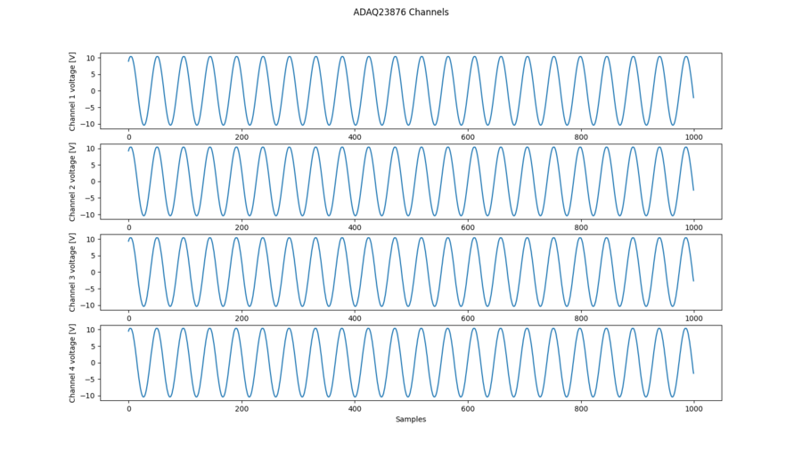
The DAC outputs should be looped back into the ADCs as shown in figure 7 in the System Setup Using a ZedBoard section. After running the script with the board in this configuration, the following window will pop up:
Important
If you plan to transmit multiple cycles of synchronous stream, make sure the script starts/stops axi-ad3552r-1 first, then axi-ad3552r-0.
MATLAB and Simulink
Download
Required MATLAB Add-Ons:
Download
Github link for the Matlab sample script: CN0585StreamingTest.m
The steps described in the matlab tranceiver-toolbox section have to be followed to configure the Matlab/Simulink project using the MathWorks HDL Workflow Advisor.
Device Control and Data Streaming
Remote data streaming to and from hardware is made available through system object interfaces, which are unique for each component or platform. The hardware interfacing system objects provide a class to both configure a given platform and move data back and forth from the device. To run the CN0585StreamingTest.m example, the following steps must be completed first.
Ensure MATLAB package “Communications Toolbox Support Package for Analog Devices ADALM-Pluto Radio” is installed from Matlab Add-Ons.
Execute the following commands on the computer terminal (Cygwin is recommended for Windows) to set up a local git repository.
~$
git clone https://github.com/analogdevicesinc/HighSpeedConverterToolbox.git
~$
cd HighSpeedConverterToolbox
~/HighSpeedConverterToolbox$
git submodule update --init --recursive
~/HighSpeedConverterToolbox$
git checkout cn0585_v1
Open Matlab from the HighSpeedConverterToolbox directory.
Open CN0585StreamingTest.m from the test subdirectory, update the board_ip variable to match the Zedboard IP address, and finally run the script.
The DAC outputs should be looped back into the ADCs as shown in figure 6 in the System Setup Using a ZedBoard section. After running the script with the board in this configuration, the window in Figure 17 will pop up.
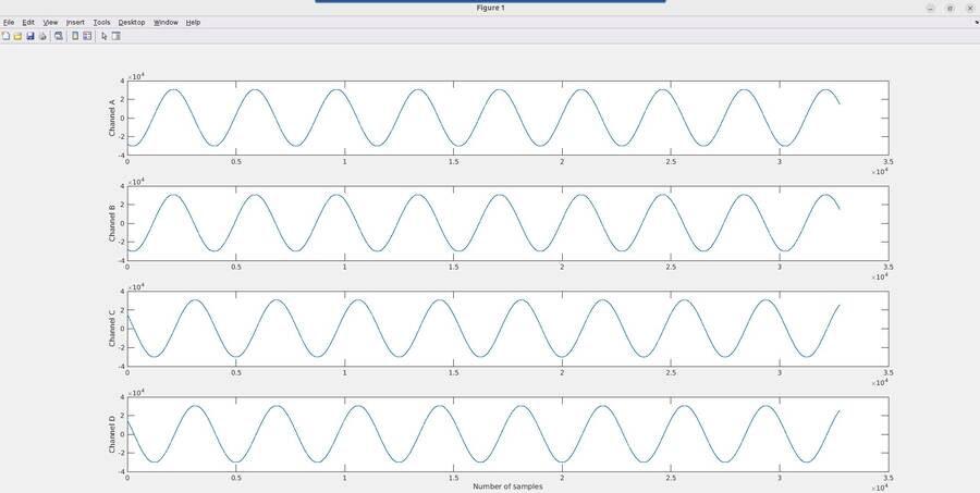
Note the y-axis is plotted in units of ADC codes, and can be converted to voltage by referencing the transfer function on the ADAQ23876 data sheet.
Important
If you plan to transmit multiple cycles of synchronous stream, make sure to start/stop axi-ad3552r-1 first, then axi-ad3552r-0.
Configuring Custom HDL Models Using Simulink
The ZedBoard that drives CN0585 is configured with a HDL reference design which is an embedded system built around a processor core either ARM, NIOS-II, or Microblaze.
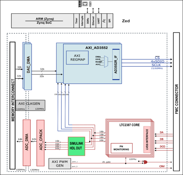
Figure 18 HDL Block Design with Simulink HDL_DUT in Rx Configuration
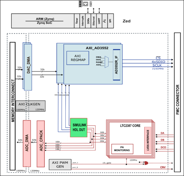
Figure 19 HDL Block Design with Simulink HDL_DUT in Tx Configuration
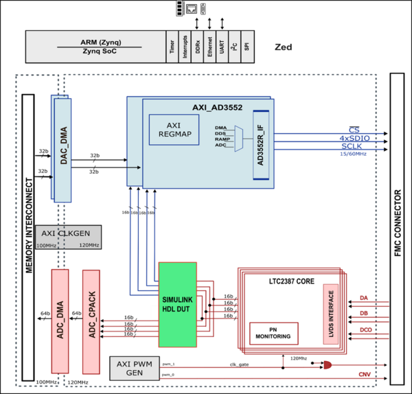
Figure 20 HDL Block Design with Simulink HDL_DUT in Rx-Tx Configuration
The device digital interface is handled by specific device cores axi_ad35552r for the DAC path and axi_ltc2387 for the ADC path. The cores are programmable through an AXI-lite interface. Details of reference design can be found in the HDL Reference Design.
HighSpeedConverterToolbox repository supports IP Core generation flow from MathWorks which allows for automated integration of HDL_DUT into HDL reference designs from Analog Devices. The workflow for generating HDL_DUT codes takes Simulink subsystems, runs HDL-Coder to generate source Verilog, and then integrates that into a larger reference design. HDL_DUT can be integrated inside HDL reference design in three different configurations which are Rx,Tx and Rx-TX. Figure 19 and Figure 20 demonstrates how HDL_DUT is placed between Tx and Rx path for these three configuration types. HDL_DUT Code Generation Workflow is described in Configuring Matlab guide.
Digital Template
For an example with a model that utilizes a wider sample of MATLAB Simulink blocks in the design, the Digital Template Model includes a Simulink model and instructions on how to use it.
Schematic, PCB Layout, Bill of Materials
Download
EVAL-CN0584-EBZ Design & Integration Files
Schematics
PCB Layout
Bill of Materials
Allegro Project
Additional Information and Useful Links
Reference Demos & Software
Help and Support
For questions and more information, please visit the EngineerZone.