Hardware User Guide
Introduction
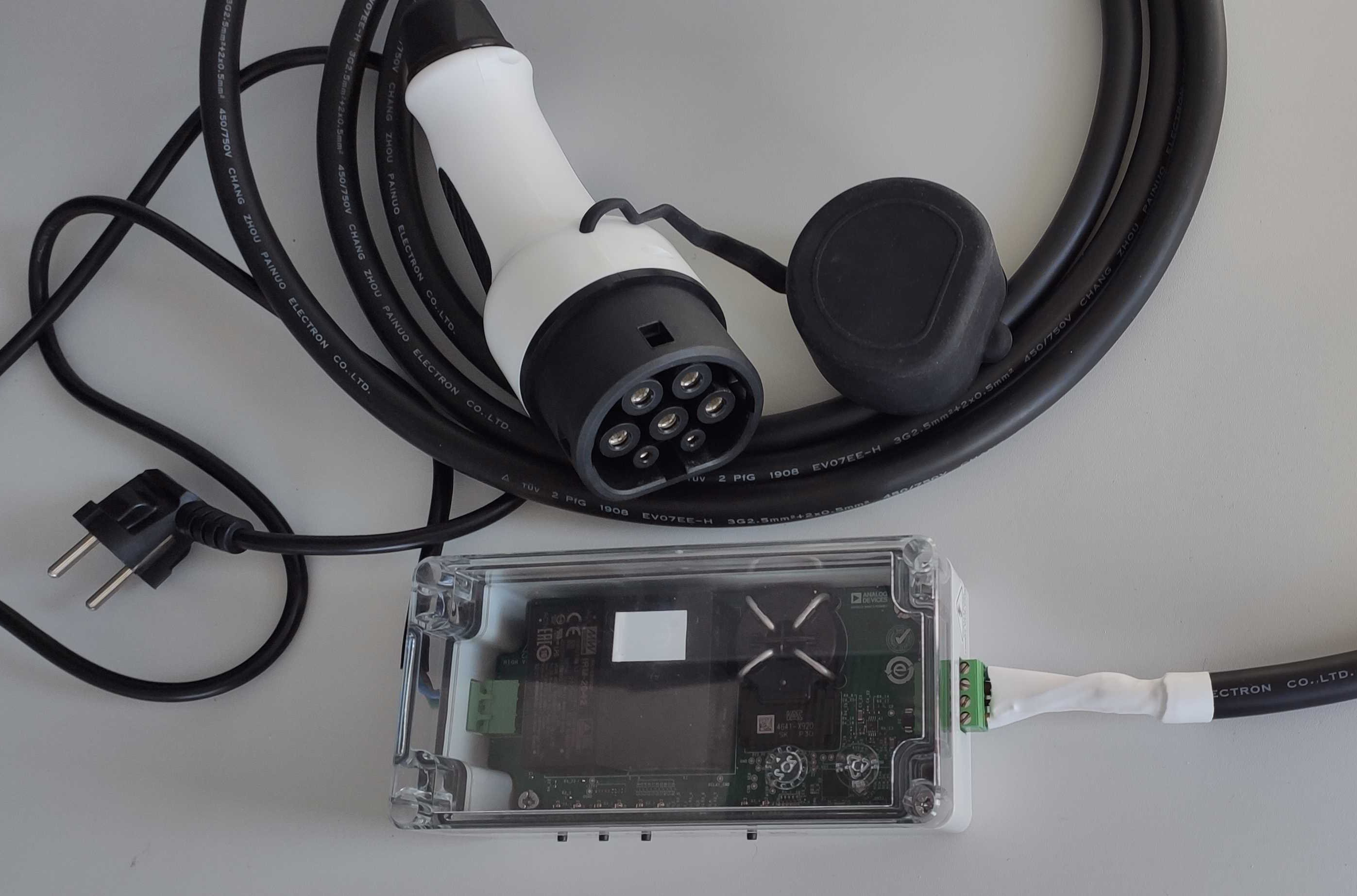
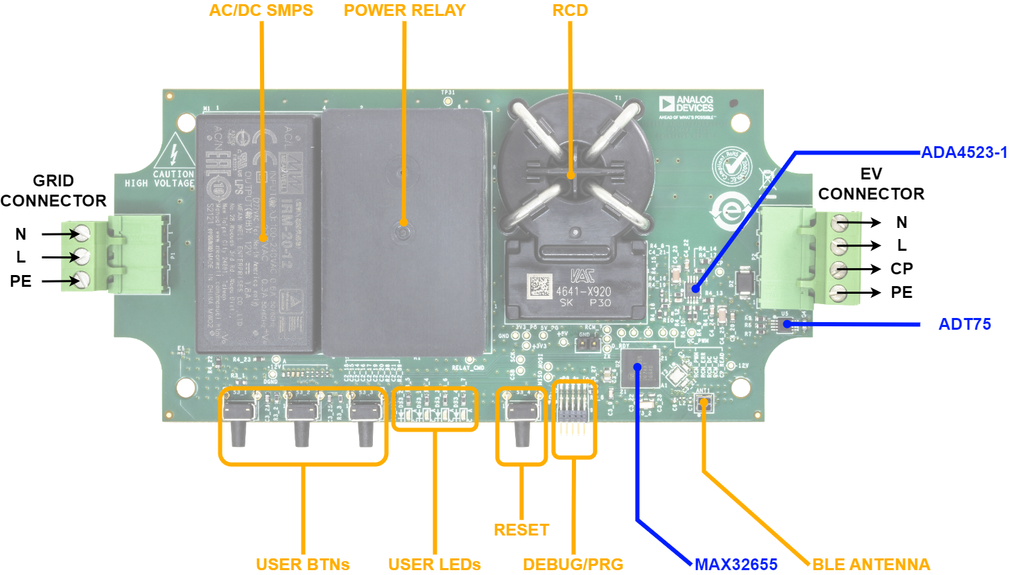
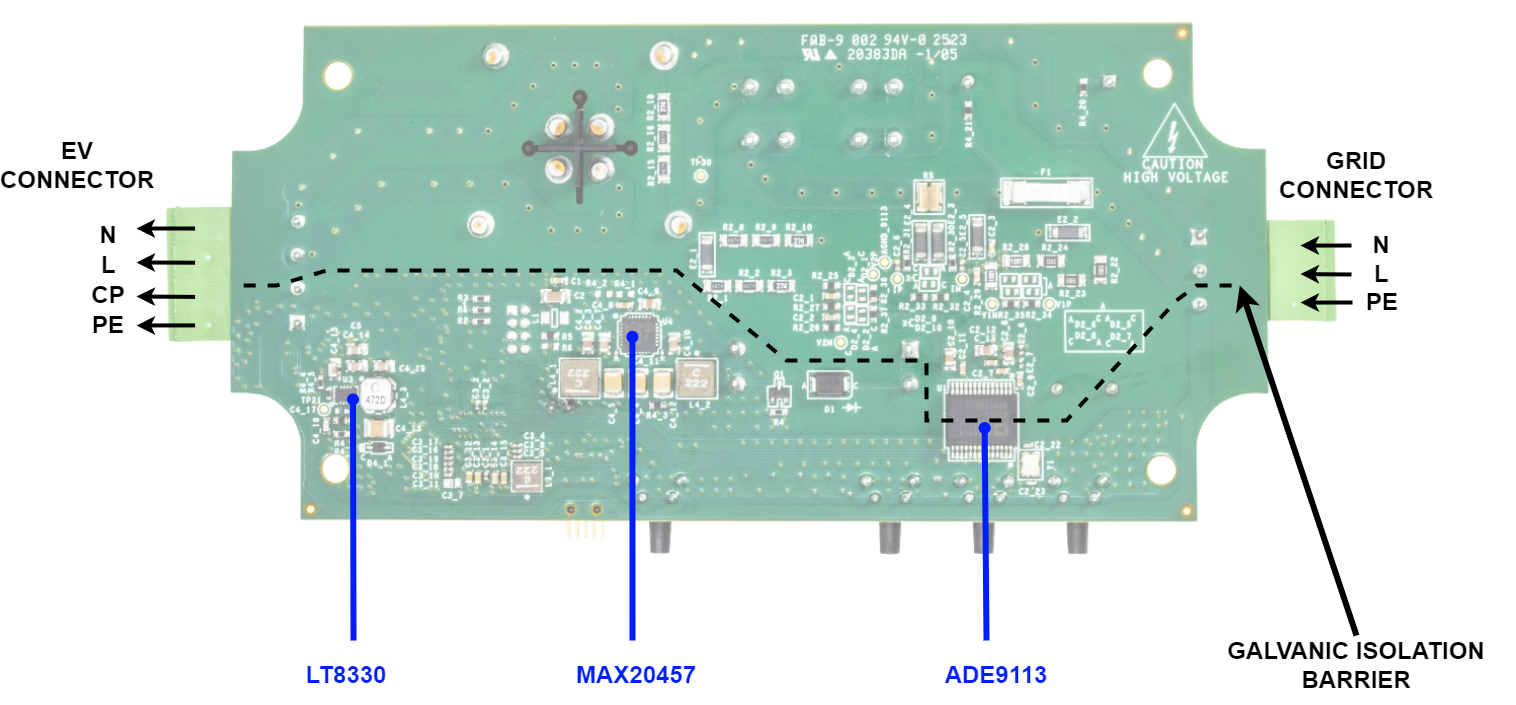
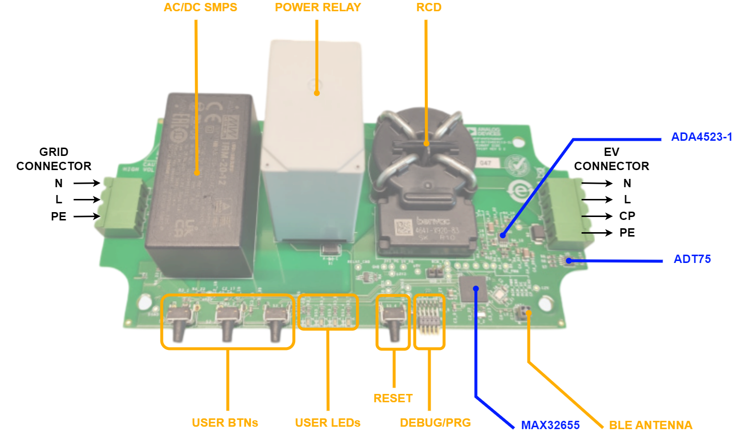
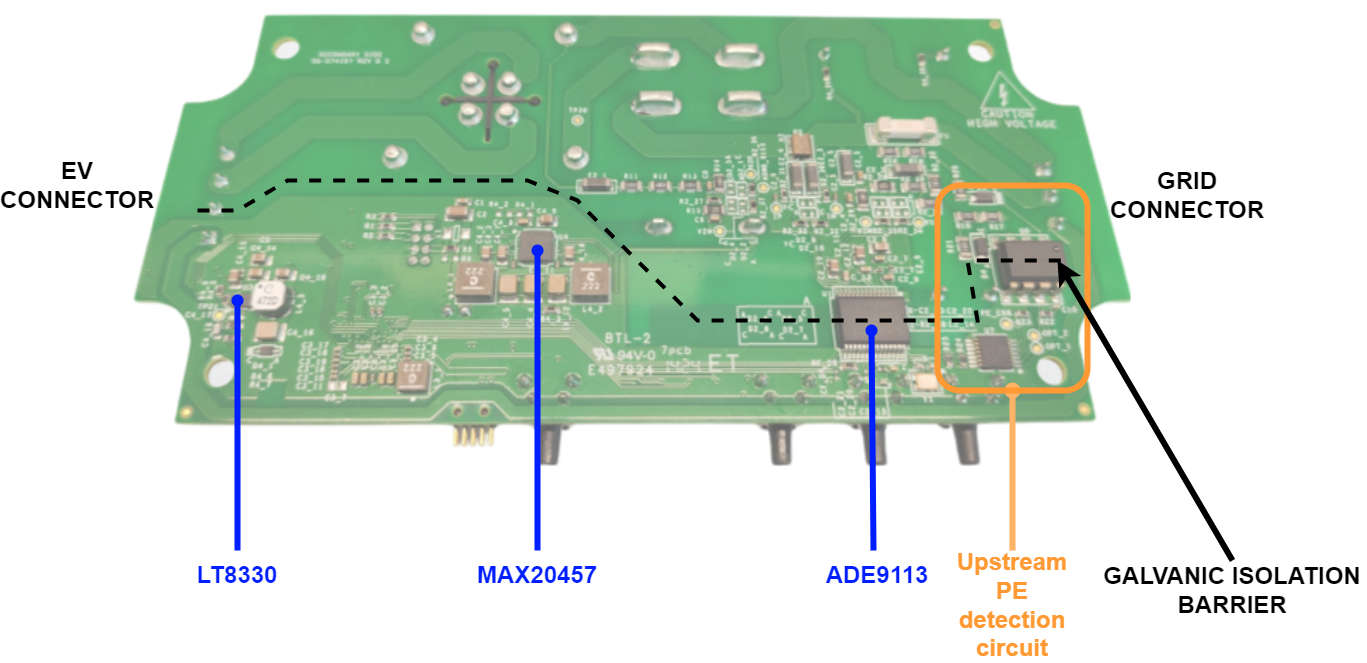
The AD-ACEVSECRDSET-SL design incorporates the ADE9113 3-Channel, Isolated, Sigma Delta (Σ-Δ) ADC and the MAX32655 low-power, Arm Cortex-M4 processor with FPU-Based microcontroller and Bluetooth 5.2 allowing the implementation of type 2 EVSE charging cables. The ADE9113 has two voltage measurement channels and a current measurement one used to implement the safety functions in the firmware. The integrated isolation makes the connection with the MAX32655 straightforward. The communication between the two components is implemented over SPI.
The control pilot (CP) signal needed for implementing the communication between the EVSE and EV is generated using the MAX32655 and the ADA4523-1 Low Noise, Zero Drift Op Amp.
The system is powered from the single phase 230V AC input. An isolated AC-DC SMPS is used to deliver 12V to the board and the MAX20457 high-efficiency dual synchronous buck converters for automotive applications are used to step down the voltage to 5V and 3.3V providing power to the isolated side of the board. The LT8330 used in the inverting configuration generates the 12V negative voltage needed for the low side of the CP signal.
The MAX32655 exposes all the necessary debug and programming features enabling a complete software development experience. The Bluetooth 5.2 LE radio with the available fully open-source Bluetooth 5.2 stack makes it easy to develop an interaction method between the user and the board. Four user buttons and 4 LEDs are also provided to complete the user interface. Serial communication (RS-232) is used for sending debug messages during testing or development.
The ADT75 12-Bit digital temperature sensor monitors the temperature of the device and sends it to the MCU unit for implementing overtemperature protection.
The main components used in the design are highlighted in the following figures.
Components
Revision A
Revision D
Setting up the board
To power up the board, connect the grid connector to a single-phase 230V AC line.
A 3-wire cable rated at 16A is the minimum acceptable. The output can be connected to
an EVSE test adapter, a type 2 cable (and EV), or left disconnected for first time power-up
or programming. The program/debug connector, which is a 10-pin ARM Cortex debug connector,
must be connected to a programmer, such as the MAX32625PICO MAXDAP DAPLink programmer
based on the MAX32625, using a cable if a firmware update is required. The MAXDAP can
also be used to read debug messages during development. Messages are sent via RS-232.
The UART device ID is 0, with the following settings: 57600 baud, 8 data bits,
no parity, 1 stop bit (57600 8N1).
The following figures show the messages received on a computer connected to the board through the MAXDAP, with the debug print option enabled.
Revision A
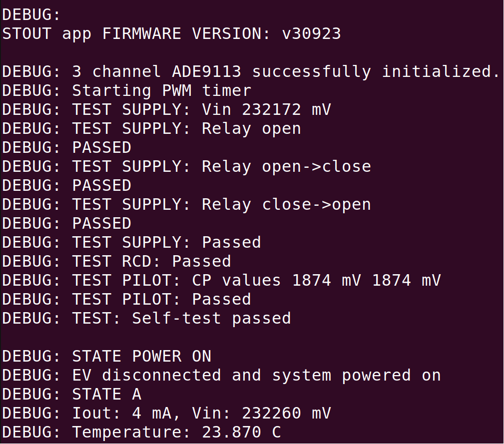
Figure 5 Rev A — Debug messages received during the self-test phase
Revision D
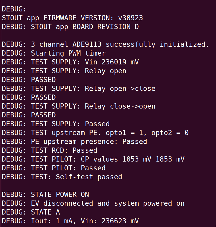
Figure 6 Rev D — Debug messages received during the self-test phase
After the self-test finishes, a charging session can be initiated by the EV or
the device connected to the EV connector. The following images present the
debug messages received during a charging session.
Revision A
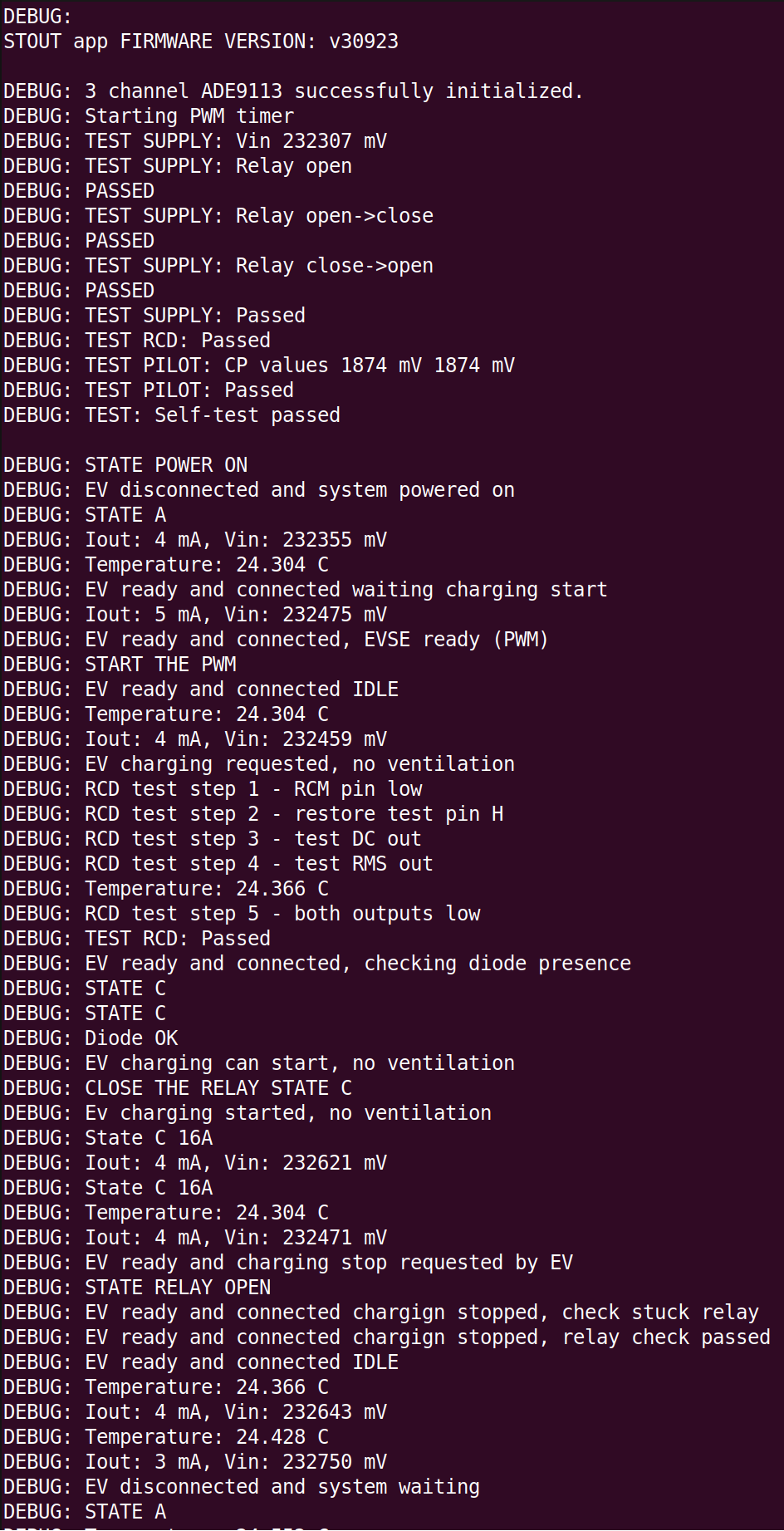
Figure 7 Rev A — Debug messages received during a charging session
Revision D
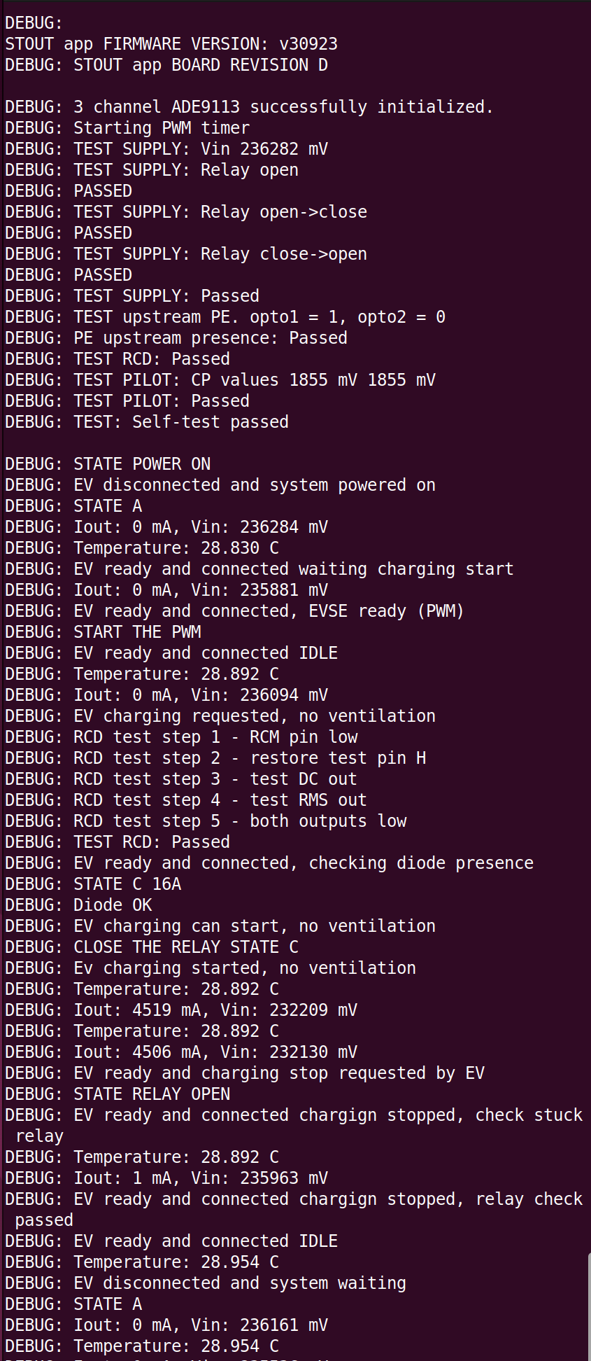
Figure 8 Rev D — Debug messages received during a charging session
User Interface
Three programable push buttons, one MCU reset button and four LEDs, are available for user interface.
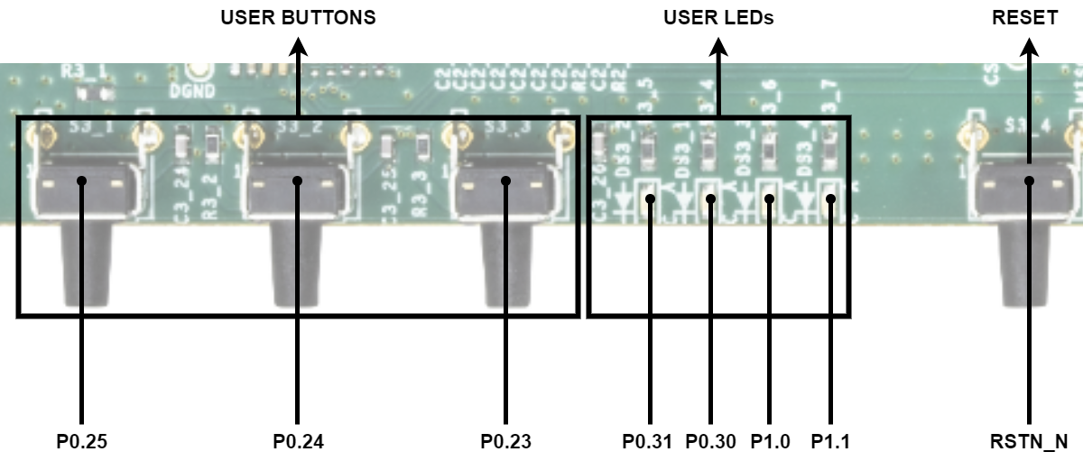
The buttons and LEDs are connected to the MCU as shown in the image above. The LEDs indicate the current state of the EVSE or display the type of error if one is detected.
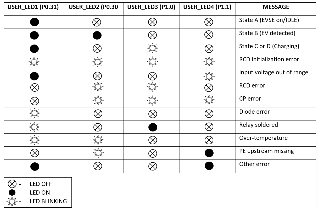
Figure 10 LEDs on the Rev D board
during state C if the LED blinks fast then the current is set at 16A, if it blinks slow it is limited to 10A
Test Points
For evaluation and debugging purpose, test points are provided at every important point on the PCB. The names of the test points are printed on the silkscreen.
Scope Images
CP signal values corelated to the EVSE states
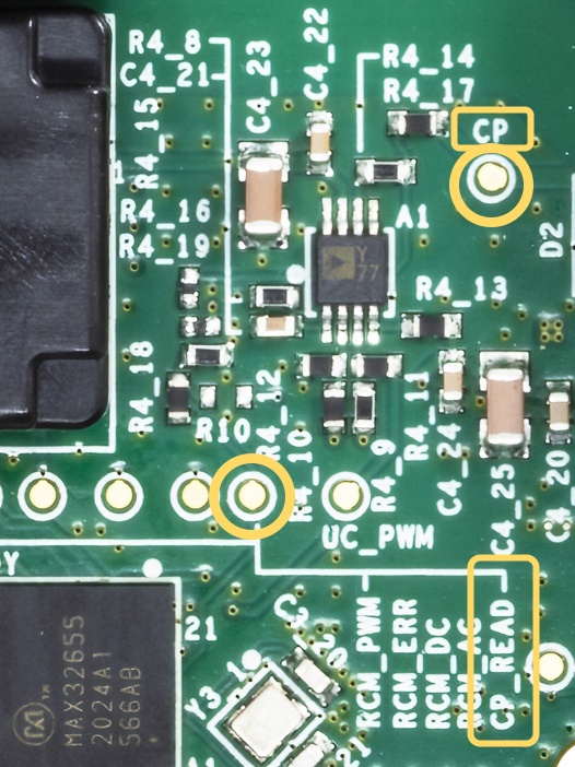
The CP signal is shown for each state (A, B, C, D, and diode error) in the following images, measured at two different points on the board. The first image for each case shows the value measured at the CP test point highlighted in the following image, and the second shows the value at the CP_READ test point, which corresponds to the MCU ADC input.
The values of the CP signal must be in the limits indicated in the next table for each state.
State |
CP signal type |
CP high value [V] |
CP low Value [V] |
Equivalent resistance [Ω] |
EV status |
|---|---|---|---|---|---|
State A |
PWM/DC |
12 [11;13] |
Not connected |
||
State B |
PWM/DC |
9 [8;10] |
-12 |
2740 |
Connected |
State C |
PWM/DC |
6 [5;7] |
-12 |
882 |
Charging, does not require charging ventilation |
State D |
PWM/DC |
3 [2;4] |
-12 |
246 |
Charging, ventilation required |
State E |
DC |
0 [-1;1] |
0 |
Fault in control circuit |
|
State F |
DC |
-12 |
Unknown fault |
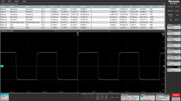
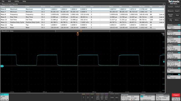
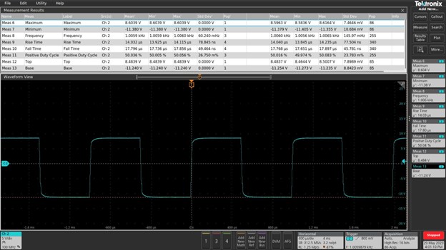

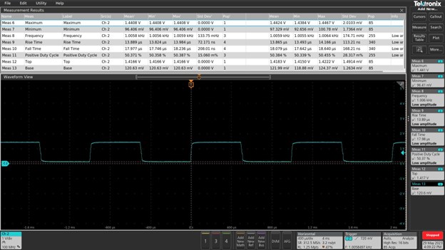
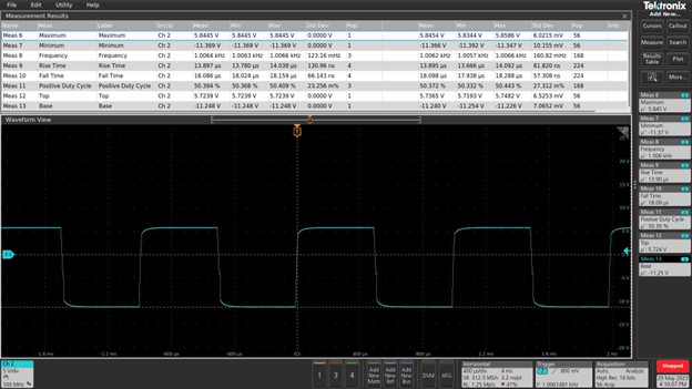

Figure 18 State D — (charging with ventilation requested) CP test point
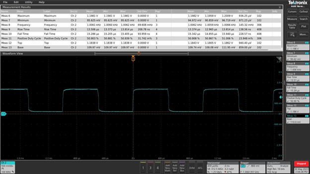

Figure 20 State diode error (EV diode missing) CP test point

Testing the EVSE
Two measurements are presented following a complete run of the state machine, from power-up to charging and EV disconnection. The tests are performed using the following test bench setup.
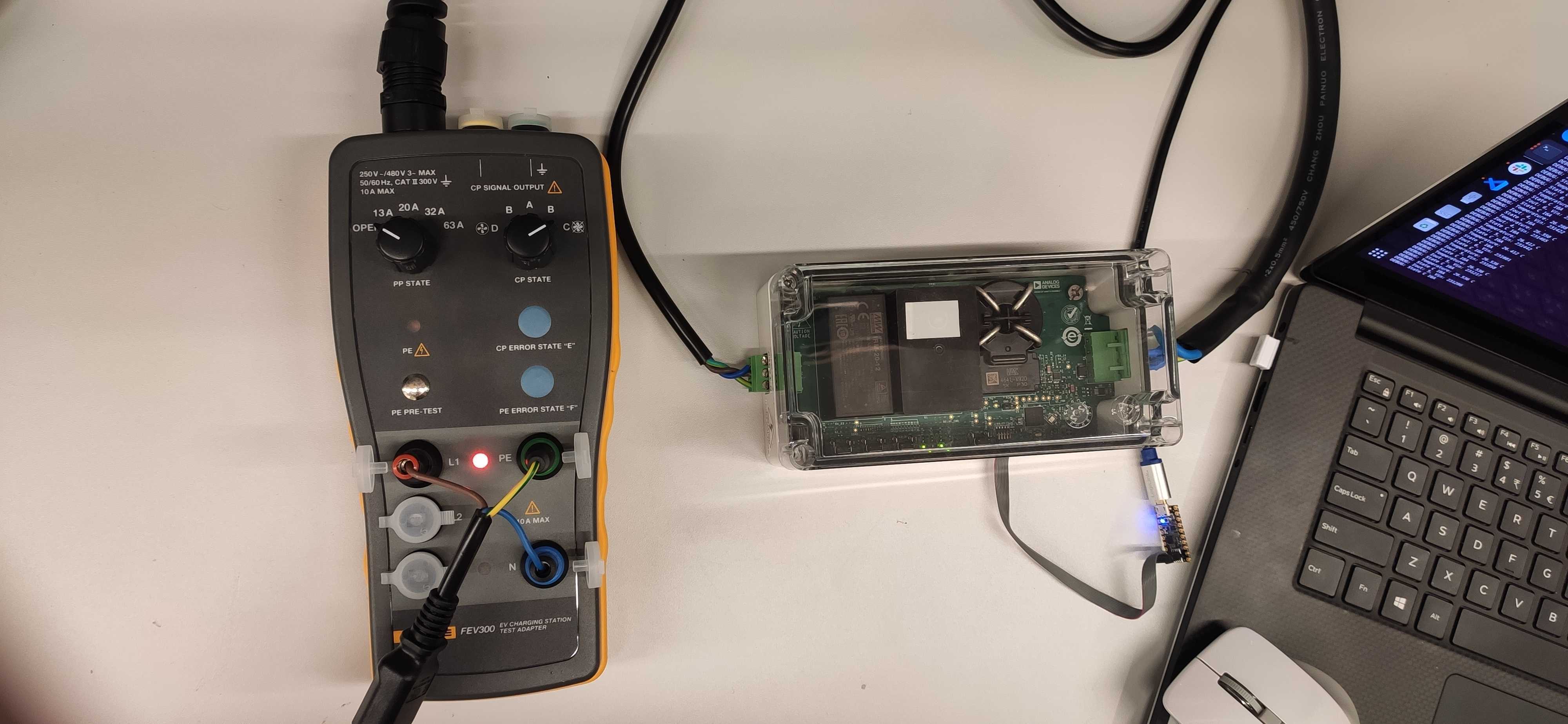
Figure 22 Normal working conditions with highlight on the EVSE-EV states
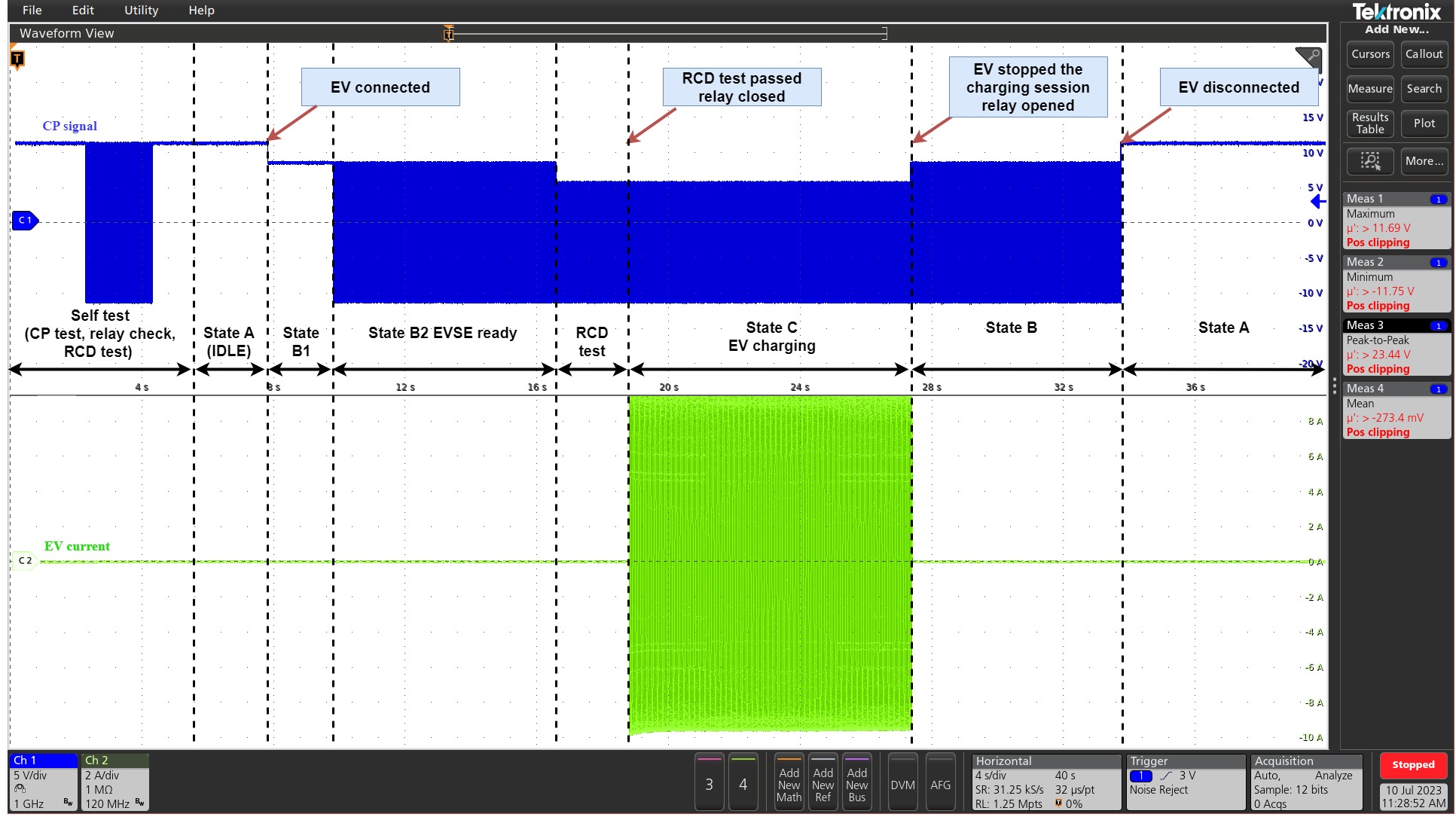
Figure 23 RCD AC error detected during a charging session in state C (charging without ventilation)
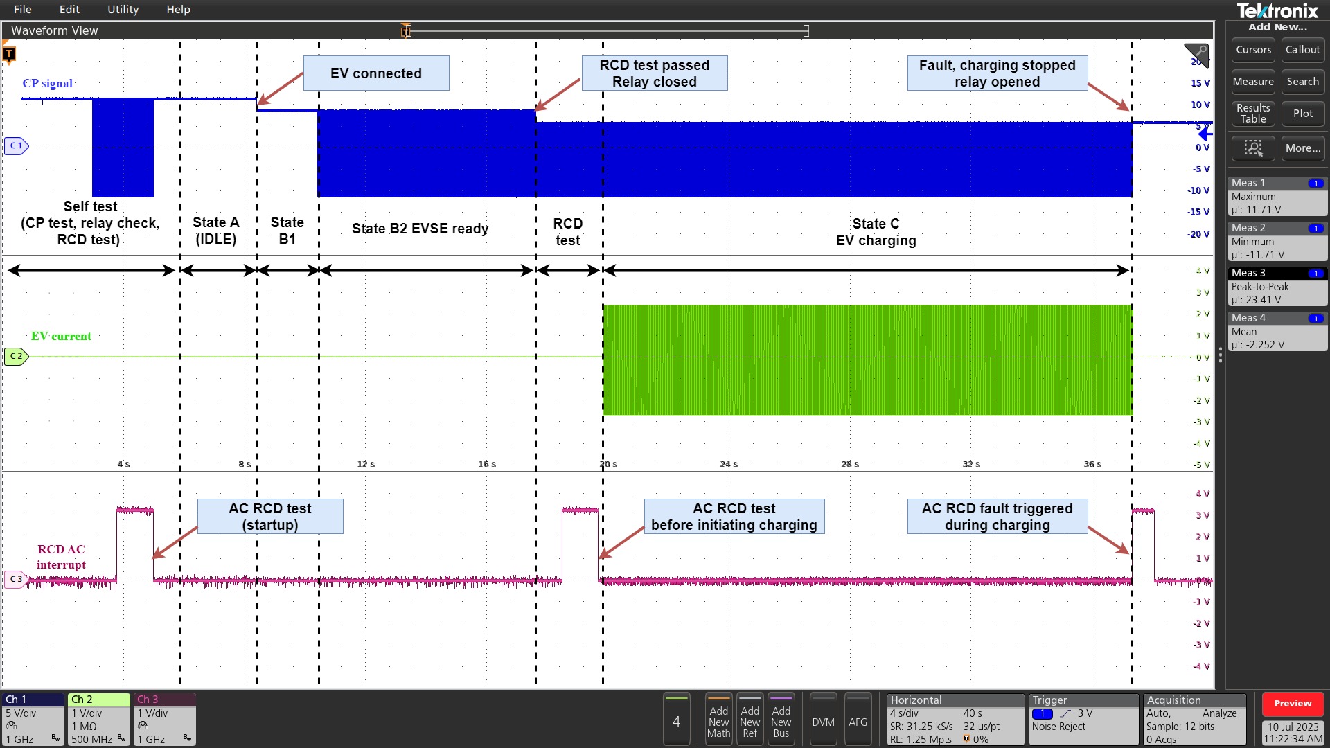
Figure 24 EVSE Setup with Type 2 cable connected on the EV side