EVAL-LTPA-KIT (LTpowerAnalyzer™ Kit)
Low-cost, High Performance, Compact Laboratory Tool for Evaluating and Characterizing Power Supply Designs
Overview
The EVAL-LTPA-KIT or LTpowerAnalyzer™ Kit is a low-cost, high performance, compact laboratory tool for evaluating and characterizing power supply designs — allowing measurements of frequency response, transient response, and output impedance. Combined with the capabilities of the ADALM2000 Active Learning Module, it offers high portability with its compact size.
The LTpowerAnalyzer™ Software offers a user-friendly interface with documentations for ease of usage. It comes with four different current probes for 1A, 10A, 50A, and 100A. Immediately kick-off using the kit with the LT8642S-based demo board as the device under test (DUT).
Features
Low-cost, high performance, compact, all-in-one, laboratory tool kit for evaluating and characterizing power designs
Capable of measuring bode response, transient response, and output impedance
Offers high portability
USB-powered device
Compatible with ADALM2000
Comes with user-friendly interfaces and documentations for both hardware and software, allowing ease of use for evaluating power supply designs
Offers four (4) current probe variations for transient measurements: 1A, 10A, 50A, and 100A
Each current probe can be used as a DC load of up to 8W in still air
Applications
Laboratory Instrumentation
System Architecture
Specifications
Parameter |
Conditions |
Min |
Max |
Units |
LTpowerAnalyzer™ Main Board (LB3031A) |
||||
DC Input Voltage |
T+, T-, OUT+, OUT-, IN+, IN-, VOUT+, VOUT- to GND to prevent damage |
±100 |
V |
|
Full Scale Signal Input Voltage |
OUT+, OUT-, IN+, IN to GND to prevent signal clipping |
±230 |
mV |
|
VOUT+, VOUT- to GND to prevent signal clipping |
±600 |
mV |
||
Bandwidth |
100 |
10M |
Hz |
|
Current Probe (LB3058A) |
||||
Max Vout Voltage |
Vout to GND |
-0.3 |
30 |
V |
Max Peak Current |
-A |
1.2 |
A |
|
-B |
12 |
A |
||
-C |
60 |
A |
||
-D |
120 |
A |
||
Min Current Rise Time |
200 |
ns |
||
Max Temperature |
Automatic Thermal Shutdown Temperature |
80 |
°C |
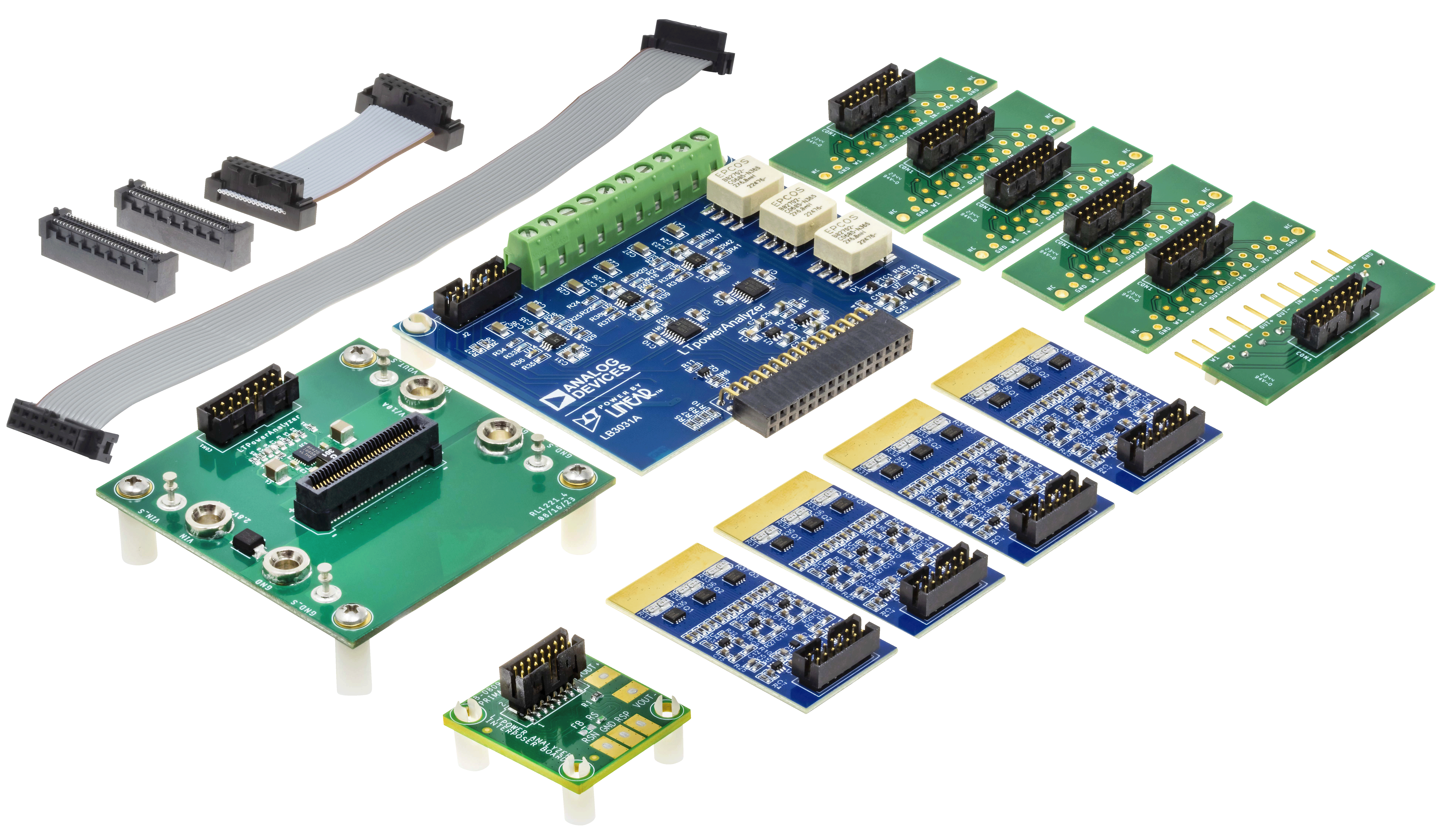
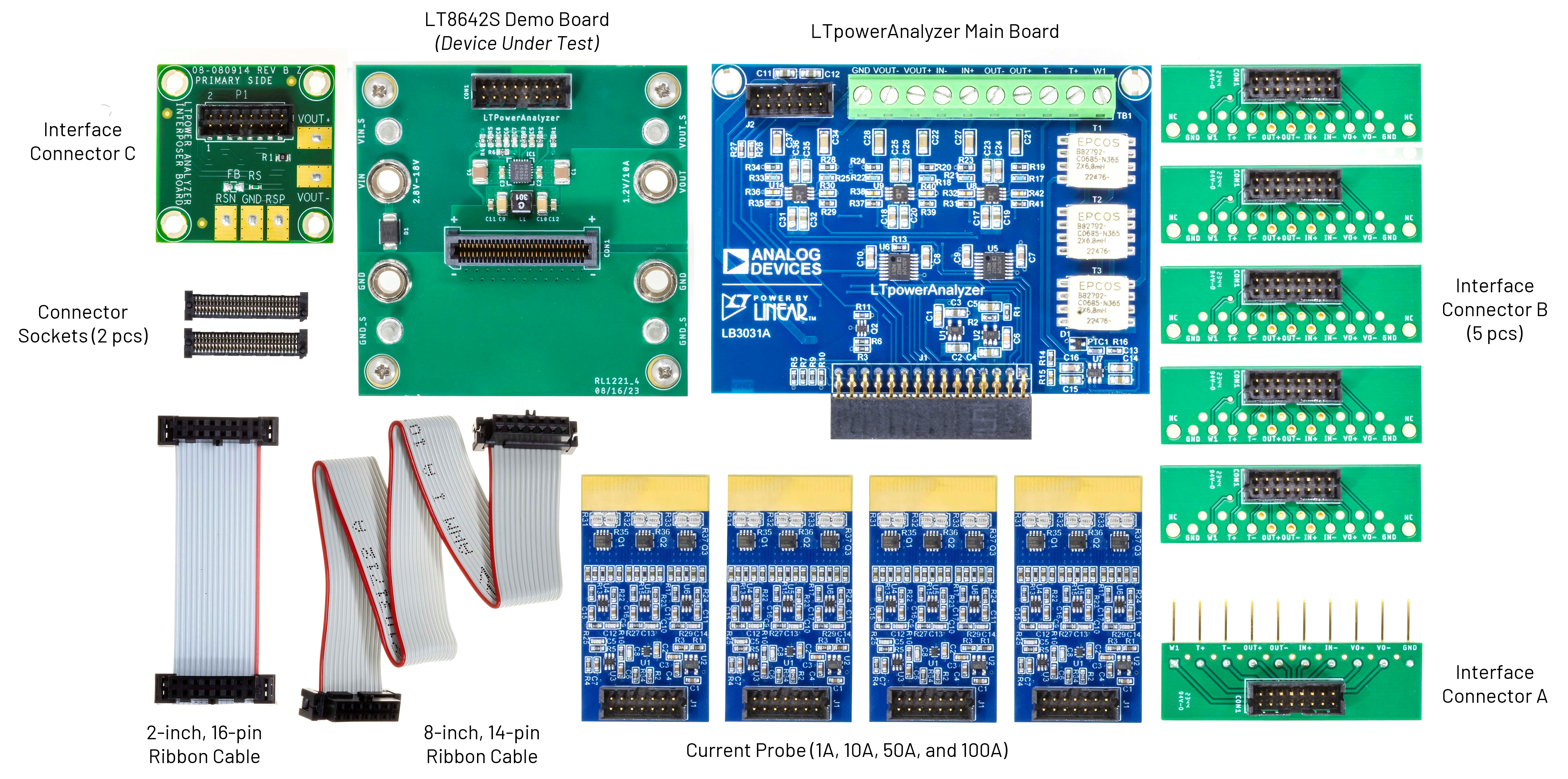
What’s Inside the Box?
The EVAL-LTPA-KIT comes with the following boards and accessories:
Components and Connections
Power Analyzer Board Connections
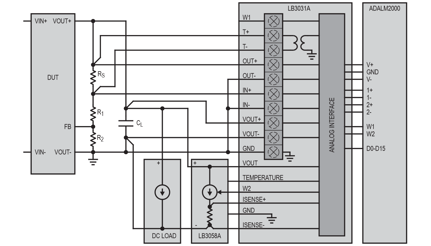
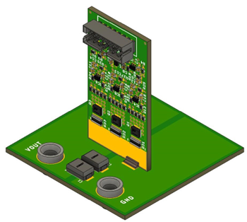
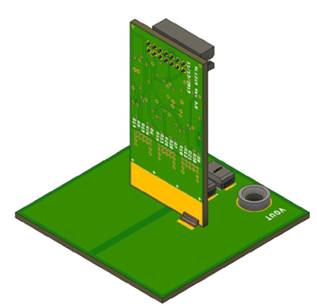
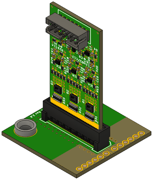
The LTpowerAnalyzer™ Main Board (LB3031A) extends the electrical capabilities of the ADALM2000 Active Learning Module (M2K) by providing an analog signal chain interface that can accommodate ±100 VDC of differential input voltage at its ports. This enables a broader range of power supply DUTs that can be evaluated with the ADALM2000.
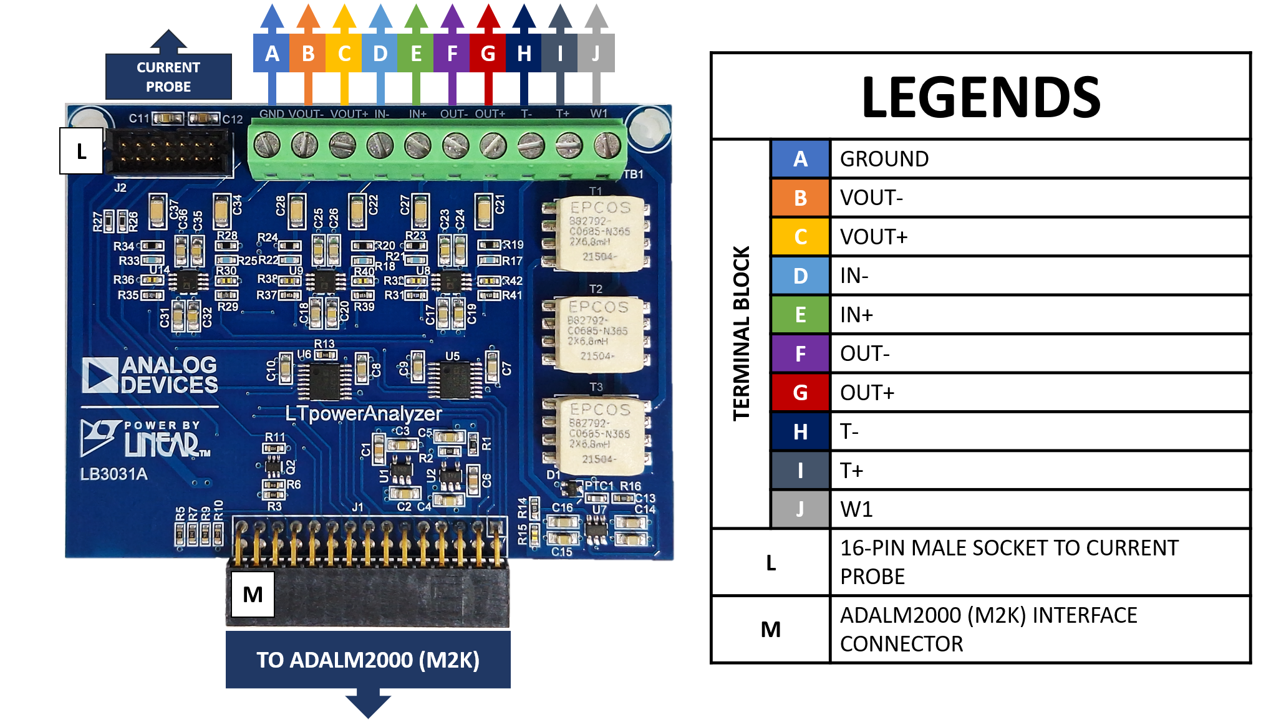
Main Board Pinout
GROUND |
Ground pin of the LTpowerAnalyzer™ Main Board |
VOUT- |
Input negative terminal pin for the DUT output voltage sensing |
VOUT+ |
Input positive terminal pin for the DUT output voltage sensing |
IN- |
Kelvin Sense Pair for the DUT input T- |
IN+ |
Kelvin Sense Pair for the DUT input T+ |
OUT- |
Kelvin Sense Pair for the DUT output VOUT- |
OUT+ |
Kelvin Sense Pair for the DUT output VOUT+ |
T- |
Output negative terminal for the Isolated Signal Injection from W1 |
T+ |
Output positive terminal for the Isolated Signal Injection from W1 |
W1 |
Pass-through for ADALM2000 W1 Waveform Generator |
Current Probe Connection
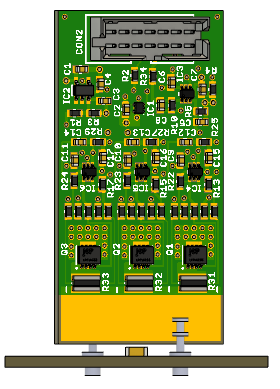
The current probes are used to generate a current pulse for the transient measurement, and a sine wave current for the impedance measurement. There are four versions of the LB3058A: 1A, 10A, 50A, and 100A full scale with a 20V maximum output voltage. Each probe has three current sources in parallel to provide a wide dynamic range and distribute the power dissipation at full scale. The probes are connected to the Power Analyzer board using a 14-pin ribbon cable, which is the same as the DC590. The probe is designed to work for positive voltages only, and the FET body diode will turn on if the + pin is pulled below -. The software will automatically recognize which probe is connected, and adjust the current range accordingly. The probes are not designed to generate a continuous DC current due to their small size.
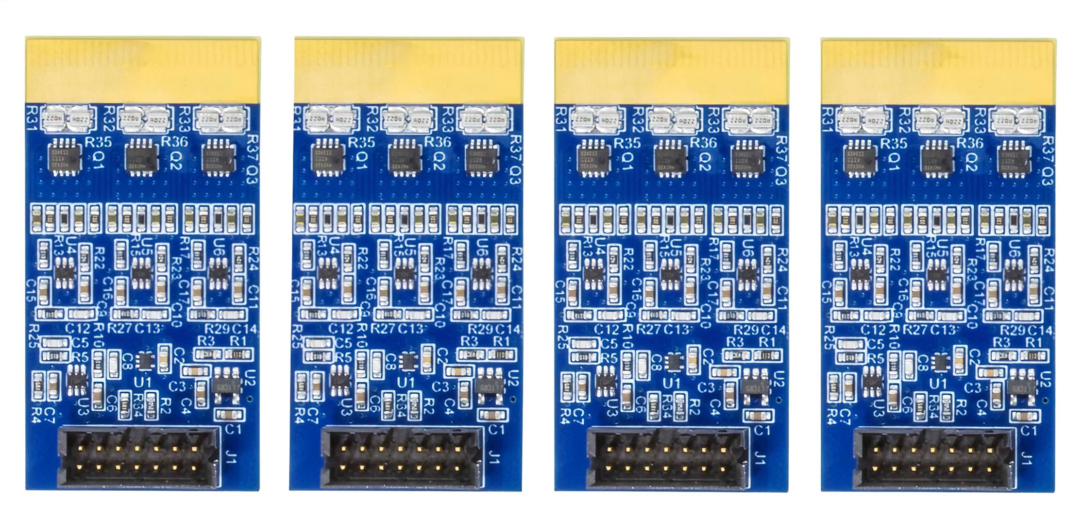
Figure 4 LB3058A Current Probe Modules: 1A, 10A, 50A, and 100A
The minimum resolution of the current probe is determined by the maximum offset of the amplifier driving the MOSFET in each of the three power stages (2 mV) and is equal to the maximum current for each power stage divided by 100. For example, the 10 A current probe has a maximum current limit of 12 A and will have the following minimum resolution:
Load Current |
Number of Power Stages Used |
Minimum Current |
0A to 3.999A |
1 |
40 mA |
4A to 7.999A |
2 |
80 mA |
8A to 12A |
3 |
120 mA |
The current probe has circuitry that measures the DUT output voltage and the board temperature. Before running a measurement, the software estimates the temperature rise of the current source FETs based on the DUT output voltage, the current waveform profile, and the measured board temperature. If the calculation predicts that the maximum safe operating area (SOA) of FETs would be exceeded, the measurement will not run.
The current probe connection to the board must be made to minimize the parasitic inductance and resistance. The best way to do this for currents > ~5A is to scrape away an opening in the solder mask on the board, then solder the probe directly to the board using a piece of solder braid folded at a 90-degree angle on either side to provide a strong mechanical connection.
For smaller currents, the probe can be connected via turrets or wire to the board. The current probe can also be mated with the 60-pin surface mount connector from Samtec, model HSEC8-130-01-S-DV-A, Digikey #SAM9504-ND. The solder mask can be scraped off and the socket soldered to the board power planes.
Standard Kelvin Connection
The Bode Plot for a typical power supply is generated by injecting a small AC signal through a transformer across a small resistor (Rs), which is inserted into the external feedback resistor string. At each frequency, the AC differential voltage at IN and OUT is measured and the gain and phase are calculated using a Fast Fourier Transform (FFT) algorithm. The typical connection ties IN- and OUT- to GND. By making the signal injector and input signal amplifiers AC-coupled, a ±100 VDC common-mode voltage can be accommodated with a frequency range of 100 Hz to 10 MHz.
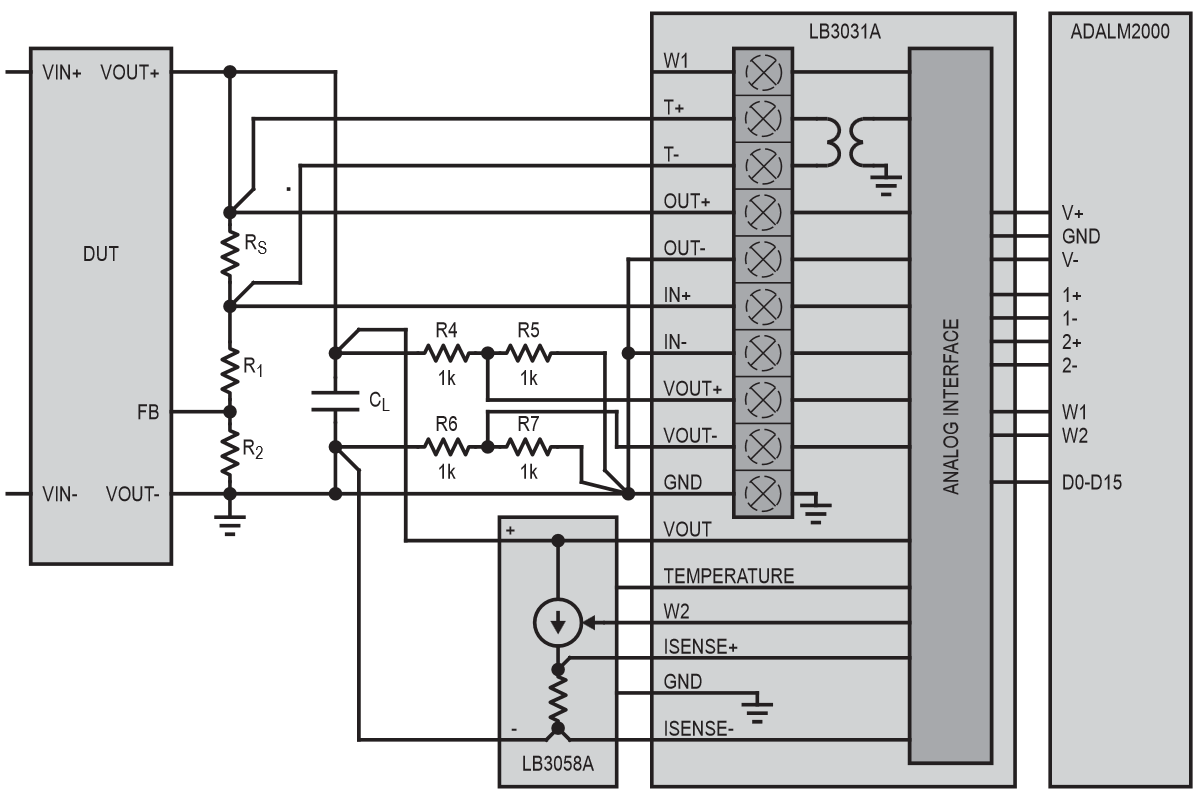
At low frequencies, the open loop gain of the supply is high, so most of the injected AC signal appears at OUT and a tiny amount at IN. At the crossover frequency, the injected signal is evenly split between IN and OUT, and at high frequencies when the gain is less than one, most of the injected signal appears at IN.
A typical setup will use short length 24 to 32 gauge twisted pair wires that are soldered directly to Rs on the DUT board, and the other ends inserted into the screw terminals on the LB3031A or the interface board. The setup requires a kelvin connection that has 4 wires (T+, OUT+, T-, IN+) connected to Rs to get the best results.
The LB3058A current probe must be connected to the DUT board with a minimum of series resistance and inductance. The output voltage for the transient and impedance measurements should be sensed directly at the output capacitors on the DUT and is measured though a fully differential signal path. The LB3058A current probe is not designed to generate a constant DC current due to its small size, so an external DC load generator will be needed for the Bode Plot and Output Impedance measurements. The transient measurement does not require an external DC load current as long as the pulse times are short.
The ground plane of the DUT must be connected to the GND pin on the terminal block.
Kelvin vs. Two-Wire Connection
An example is shown below where 6-inches of 30 gauge twisted pair wire was used for the two-wire and kelvin connections.
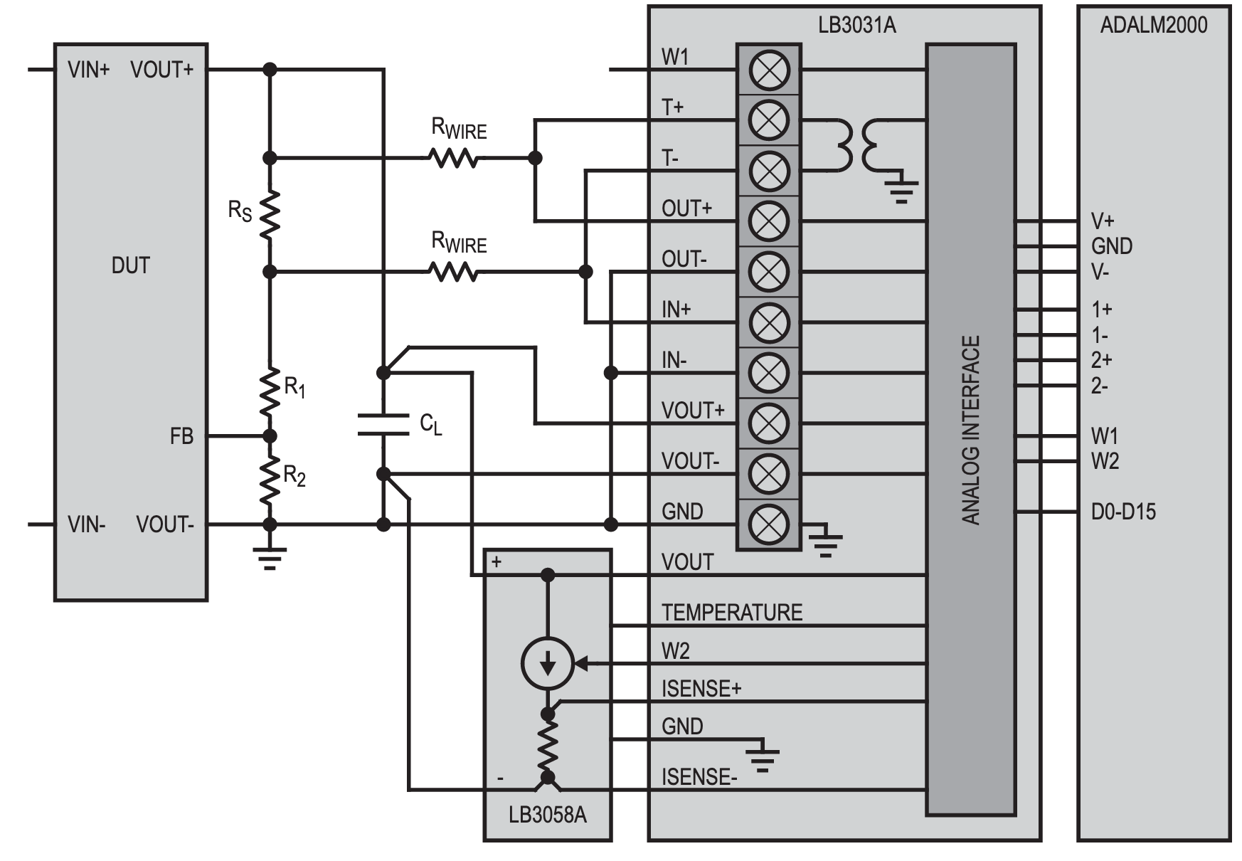
The results below 5 kHz are quite different because the voltage drop across the wires swamps out the signal at the input, which is very low because of the high open loop gain. The two sweeps merge as the open loop gain drops and the input signal level increases. Notice however, that the phase margin and gain margin are the same for the two sweeps.
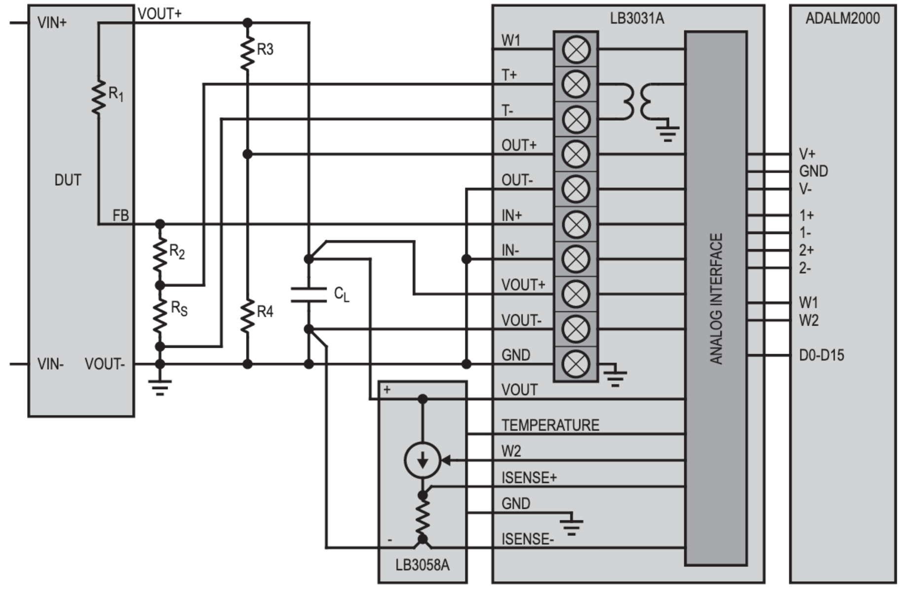
Module Connection
Many power modules include the top side feedback resistor R1 inside the package, requiring only one external Many power modules include the top side feedback resistor R1 inside the package, requiring only one external resistor R2 to set the output voltage. In this case, the injection resistor Rs cannot be inserted at the top of the feedback network but is instead connected to ground at the bottom.
To measure the true loop gain, another dummy resistor divider, R3 and R4, is connected to the output. The ratio of R3/R4 must be the same as the ratio of R1/R2. The problem with this topology is that many network analyzers have up to 50 pF of input capacitance, which forms a pole at the R3/R4 connection point. This can lead to gain and phase errors when the frequency reaches the 50 kHz to 1 MHz range, depending on the absolute value of R3 and R4. The best practice is to reduce the absolute value or R3 compared to R1, and R4 compared to R2 by a factor of 10 to 100, pushing the pole out to beyond the frequencies of interest. The input impedance of the LTpowerAnalyzer™ is about 1 pF in parallel with 1 MΩ, which should minimize this problem.
Follow below configuration to set up the system using Module Connection:
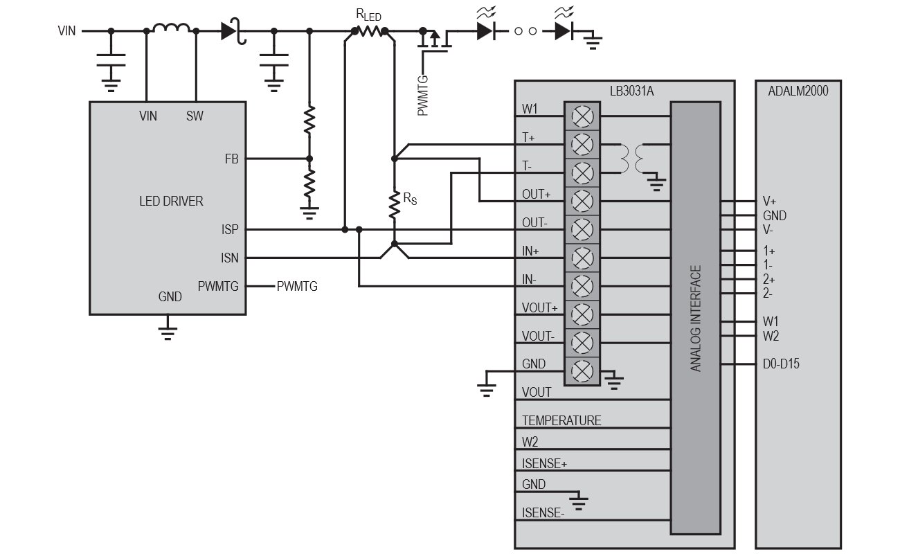
LED Driver Connection
In this type of connection, the test voltage is injected across Rs which is in series with the ISN current sense line, and input and output voltage must be measured differentially from the respective Rs connection to the ISP current sense line.
The common-mode range of the LTPowerAnalyzer™ is ±100V, and Rs is typically 20Ω to 40Ω.
Getting Started
Please refer to the following pages for detailed instructions on how to set up the LTpowerAnalyzer™ system for evaluation.
Help and Support
For questions and more information, please visit the Analog Devices EngineerZone Support Community.