Digital Template Model
A digital template is provided as a starting point for designs. There are four subsystems within this model: a DDS, a mixer, a FIR filter, and a PID controller.
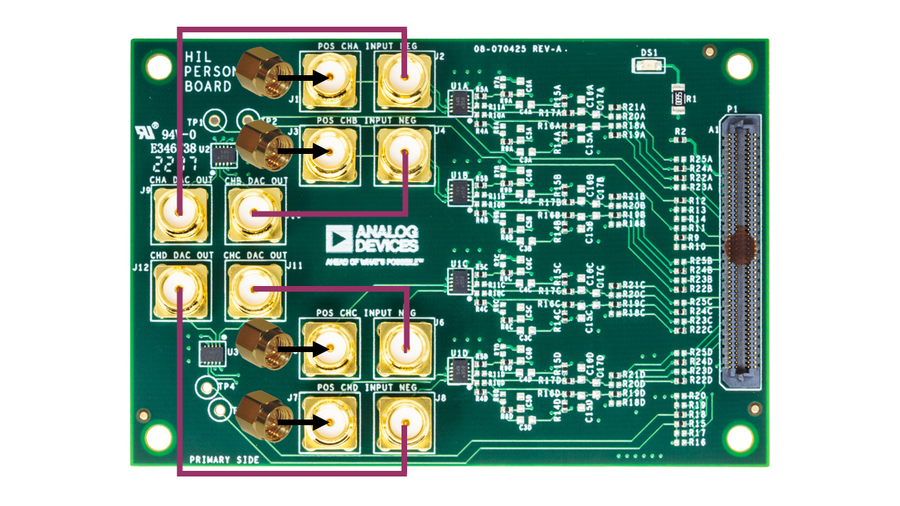
Python scripts are provided that showcase each subsystem. These scripts are designed to run with the ADCs and DACs connected in loopback mode, as described in the example Setting Up the Hardware Section, and shown in the following image.
The additional packages required to run these scripts are: scipy.fft, scipy.signal.
External signals can be used as inputs to the ADCs if desired, needed changes are explained in each section.
The ad3552r_0.output_range should be updated in each script to match the configuration of the board being used, but is default set to +10V/-10V. Each script produces a set of Python plots and terminal outputs. The terminal outputs display the configurations that were set, followed by additional measurements calculated specific to each model.
The parameters for each subsystem are controlled by AXI registers. The AXI register are 32-bits, but can be used for a variety of datatypes including int16 and fixed point decimals. Each parameter is described in the following sections with its datatype and possible range of values for the user to modify as desired.
Note
All ADC and DAC numbers are 0-indexed. For example, the 4 DACs are labeled DAC0, DAC1, DAC2 and DAC3. Same applies to ADCs.
Files
The simulink model files can be downloaded from this zip file Simulink models and placed in the HighSpeedConverterToolbox/test folder. The PID and DDS are submodels within the top level testModel_template_top.slx file, and the path pointing to the submodels should be updated to reflect the new correct path on the user’s machine. See the Build section at the bottom of tutorial for instructions on implementing the model. Additionally, the bootfile is provided here Boot file and can be copied directly into the boot directory of the SD card.
The Python example scripts can be downloaded from this zip file Python Examples, and placed in the pyadi-iio/examples folder while in the cn0585_v1 branch.
The following sections describe the model and scripts in more detail.
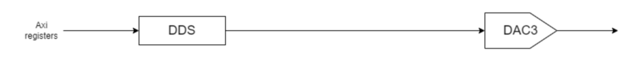
DDS
One subsystem in the model is a Direct Digital Synthesizer (DDS) that outputs a sine wave. This signal outputs on DAC3.
Run
To see the DDS in action, run the provided python script cn0585_fmcz_example_dds.py the same way the generic cn0585_fmcz_example.py script is run.
The following lines should be observed in the terminal after completion:
$ python examples/cn0585_fmcz_example_dds.py ip:169.254.92.202
uri: ip:169.254.92.202
#############################################
GPIO4_VIO state is: 0
GPIO5_VIO state is: 0
Voltage monitor values:
Temperature: 41.25 C
Channel 0: 2274.1699200119997 millivolts
Channel 1: 643.310546348 millivolts
Channel 2: 2017.822263972 millivolts
Channel 3: 763.5498040619999 millivolts
Channel 4: 2082.519529544 millivolts
Channel 5: 2090.4540998499997 millivolts
Channel 6: 2259.521482524 millivolts
Channel 7: 1806.030271958 millivolts
Buffer size is 1048576
Sampling rate is: 15000000
input_source:dac0: adc_input
input_source:dac1: adc_input
#############################################
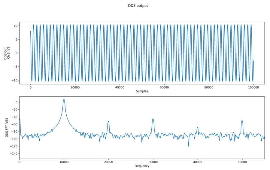
DDS frequency set to 10000 Hz
DDS amplitude set to 9.99969482421875 V
DDS phase shift set to 0 degrees
The last printed section displays what the parameter values were set to in the AXI registers. These can be compared to the Python plot for accuracy.
In addition, the following window will pop up. This displays the voltage data captured at ADC3 in the top plot, and the corresponding spectrum done by FFT (Fast Fourier Transform) of the data in the bottom plot.
Parameters
The parameters for the DDS can be found on lines 14-18 as so:
# user inputs
freq = 10000
amp = 2**15-1
phase_shift = 0
external_signals = 0
The freq variable controls the output frequency of the DDS, this can range from 0 to 1000000 in steps of 1, the units are Hertz. The amp variable controls the amplitude of the sine wave, in units of DAC codes, with a maximum value of 32767, or 2^15-1, in steps of 1. The conversion between DAC codes and voltage can be found on the AD3552R datasheet. The phase_shift offsets the sine wave phase, from -360 to 360 in steps of 1, in units of degrees. The external_signals variable should be set to 0 when the ADCs and DACs are connected in loopback mode, and set to 1 when the signals are being driven and measured with external devices. See following section for more details on hardware connections.
External Inputs and Outputs
There are no external inputs on this system. The output of the DDS can be seen by connecting DAC3 to the desired system.
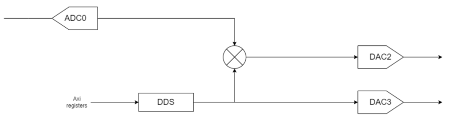
Mixer
The mixer takes one input from ADC0 and multiplies it with the output of the DDS. In loopback mode, the signal into ADC0 is generated from the DMA of DAC0. The output of the mixer goes to DAC2.
Run
The script cn0585_fmcz_example_dds_mixer.py is an example of how to see the mixer output. Run this the same way as the other example scripts. After running, the following output should be seen in the terminal.
$ python examples/cn0585_fmcz_example_dds_mixer.py ip:169.254.92.202
uri: ip:169.254.92.202
#############################################
GPIO4_VIO state is: 0
GPIO5_VIO state is: 0
Voltage monitor values:
Temperature:  47.75  C
Channel 0:  2274.780271574  millivolts
Channel 1:  644.5312494719999  millivolts
Channel 2:  2012.329099914  millivolts
Channel 3:  763.5498040619999  millivolts
Channel 4:  2079.467771734  millivolts
Channel 5:  2084.960935792  millivolts
Channel 6:  2257.690427838  millivolts
Channel 7:  1806.030271958  millivolts
Buffer size is  150000
Sampling rate is: 15000000
input_source:dac0: dma_input
input_source:dac1: adc_input
#############################################
DDS frequency set to  2000 Hz
DDS amplitude set to  0.3125 V
DDS phase shift set to  0 degrees
DMA frequency set to  3000 Hz
DMA amplitude set to  0.0390625 V
The mixer output's largest frequency component is at  5.0 kHz, with estimated signal power  13.82  dB
The last section of the terminal output displays the settings of the two input waves, as well as the largest frequency component of the mixer output.
The below window will pop up. The first plot shows the DDS output captured on ADC3, and the second plot shows the input on ADC0. The final two plots show the mixer output looped back and captured from ADC2, and its FFT transformation.
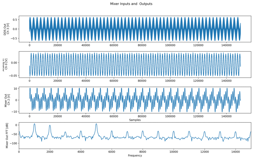
Figure 5 Mixer inputs from DDS and ADC0 (top 2 graphs), Mixer out and its FFT (bottom 2 graphs)
Parameters
The parameters used are similar to those for the DDS example, and can be found on lines 13-18.
# user inputs
dds_freq = 2000
dma_freq = 3000
dds_amp = 2**10
dma_amp = 2**7
dds_phase_shift = 0
external_signals = 0
The units are as described in the DDS section, but here are labeled with whether they control the output of the DDS- or DMA-generated sine wave. Note the DMA-generated wave does not have a phase shift option. The external_signals variable should be set to 0 when the ADCs and DACs are connected in loopback mode, and set to 1 when the signals are being driven and measured with external devices. See following section for more details on hardware connections.
External Inputs and Outputs
To use external inputs or outputs, connect an analog input signal to ADC0. The output of the mixer on DAC2 can then be connected to a desired measurement device or system.
FIR Filter
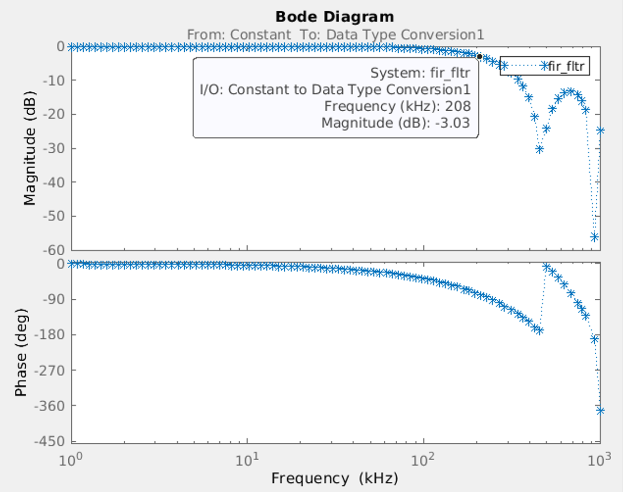
The FIR filter is implemented as a moving average filter with 32 taps. The cutoff frequency of the filter is at 200kHz. The simulated frequency response of the filter is shown below.
In loopback mode, a noisy test signal is generated from the DMA of DAC3 then fed to ADC3. The filter takes the input from ADC3, and outputs the filtered signal on DAC0.

Run
Run the cn0585_fmcz_example_fir_filter.py script the same way as the other scripts. The signal into the FIR filter is generated as a 10kHz signal, superimposed with 800kHz and random noise, the latter two of which should be reduced after being filtered.
The terminal output should resemble the following.
$ python examples/cn0585_fmcz_example_fir_filter.py ip:169.254.92.202
uri: ip:169.254.92.202
#############################################
GPIO4_VIO state is: 0
GPIO5_VIO state is: 0
Voltage monitor values:
Temperature:  47.75  C
Channel 0:  2274.780271574  millivolts
Channel 1:  643.92089791  millivolts
Channel 2:  2000.7324202359998  millivolts
Channel 3:  764.1601556239999  millivolts
Channel 4:  2072.7539045519998  millivolts
Channel 5:  2075.805662362  millivolts
Channel 6:  2257.080076276  millivolts
Channel 7:  1806.030271958  millivolts
Buffer size is  4096
Sampling rate is: 15000000
input_source:dac0: adc_input
input_source:dac1: dma_input
#############################################
SNR of unfiltered signal:  10.699287492673212 dB
SNR of filtered signal:  24.032664229257037 dB
The signal at  800039 Hz was attenuated by  17.553201089520595 dB
The last section shows the calculated signal to noise ratio of the signal pre- and post-filter. The filtered signal should have a better SNR. The attenuation of the 800kHz is also shown, a frequency which is in the cutoff region and should be substantially attenuated.
And the window with the below plots should pop up. The input to the FIR filter and its FFT are displayed in the first and third plots, while the filter output and its FFT are in the second and fourth.
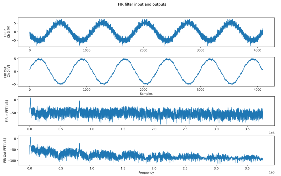
Figure 8 FIR filter output in plots 2 and 4, from the input captures in plots 1 and 3
Parameters
The only parameter in this model is the external_signals variable on line 14 of the script.
The external_signals variable should be set to 0 when the ADCs and DACs are connected in loopback mode, and set to 1 when the signals are being driven and measured with external devices. See following section for more details on hardware connections.
External Inputs and Outputs
An input analog signal can be connected to ADC3 to go into the filter, and the filter output can be taken from DAC0.
PID
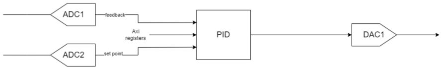
The PID controller has the set point and feedback inputs on ADC2 and ADC1 respectively, with the output on DAC1. Figure 8 shows the isolated system in the board. Figure 9 shows a closed loop example using a voltage divider as a plant.
External Inputs and Outputs
This design is intended to be used with an external plant, and as such is expected to always use external signals. ADC2 should be driven by the desired set point. To add a plant to the PID controller, connected the PID output on DAC1 to the input of the plant. Then the output of the plant must be connected to the feedback point on ADC1.
Figure 10 shows an example of using voltage divider as plant. It is composed of two 3k-Ohm resistors in series, connecting PID output at DAC1 to ground. The connection point between the resistors the connects to the feedback point at ADC1. The set point is driven by a +/-4V square wave.
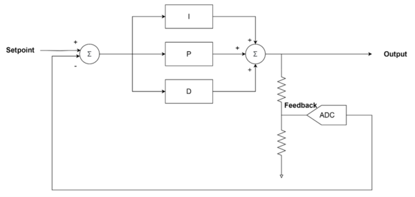
Figure 10 PID subsystem diagram with resistor divider connected as plant forming a closed loop system
Run
Run the cn0585_fmcz_example_pid.py script as the other scripts. Cite above closed loop system as example, the signal into setpoint is a square wave generated from external function generator.
The terminal output should resemble the following.
$ python examples/cn0585_fmcz_example_pid.py ip:169.254.92.202
#############################################
GPIO4_VIO state is: 0
GPIO5_VIO state is: 0
Voltage monitor values:
Temperature:  48.0  C
Channel 0:  2269.2871075159997  millivolts
Channel 1:  649.4140619679999  millivolts
Channel 2:  2052.001951444  millivolts
Channel 3:  764.1601556239999  millivolts
Channel 4:  2086.181638916  millivolts
Channel 5:  2081.909177982  millivolts
Channel 6:  2252.19726378  millivolts
Channel 7:  1798.706053214  millivolts
Buffer size is  20000
Sampling rate is: 15000000
input_source:dac0: adc_input
input_source:dac1: dma_input
#############################################
PID controller Kp given as:  1
PID controller Ki given as:  0.2
PID controller Kd given as:  0.01
Register value for kp: 1024 decimal value:  1.0
Register value for ki: 204 decimal value:  0.19921875
Register value for kd: 10 decimal value:  0.009765625
And the window with the below plots should pop up. The input to the set point is displayed on top graph, it’s a 500Hz square wave with -/+4V amplitude. The bottom graph is the feedback which resembles the set point with some overshoot feature and small latency.
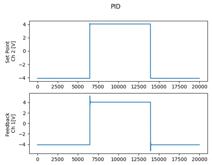
Figure 11 Setpoint of PID in top plot, feedback in bottom plot
The following figure shows the two signals on an oscilloscope with clear PID features shown.
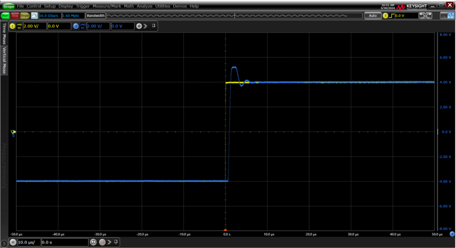
Figure 12 Example PID controller test result. Channel 1 (yellow) is setpoint, Channel 3 (blue) is feedback after going through voltage divider plant
Parameters
The parameters can be found on lines 15-17 as shown below. Kp, Ki, and Kd are respectively the proportional, integral, and derivative coefficients. All three coefficients are unsigned fixed point numbers with 6 bits of integers and 10 decimal bits.
# user inputs
Kp = 1
Ki = 0.2
Kd = 0.01
Build
After the HighSpeedConvertToolbox repo is set up on the machine as described in the Matlab Configuration Guide page of the wiki and the digital template models have been put in the correct folder, the Simulink model can be opened and built. This mostly follows the step on MATLAB Configuration, but a few changes are required.
Before starting the build process, go to Configuration Parameters -> HDL Code Generation -> Global Settings and set the Reset Type to Synchronous.
Open the HDL Workflow Advisor and start the build process as described in the Matlab Configuration Guide.
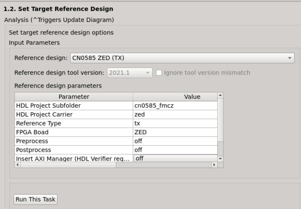
In step 1.2, the reference design should be selected as TX.
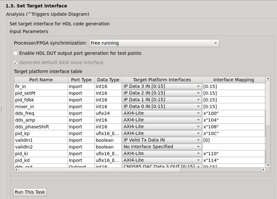
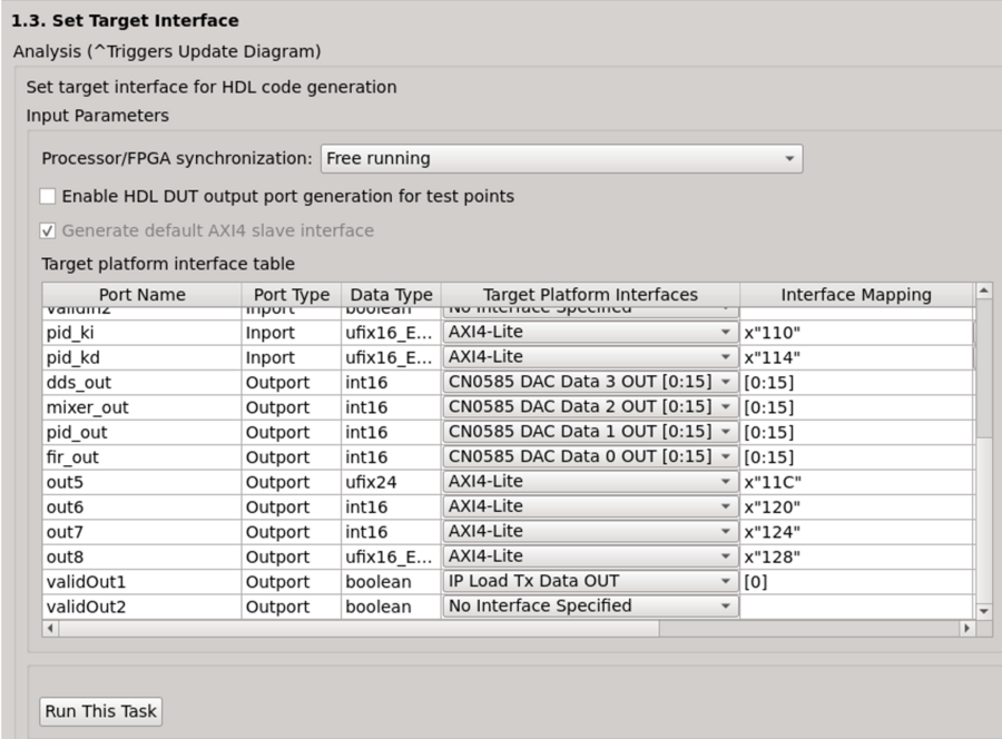
In step 1.3, ensure the connections are configured to match the screenshots below.
In step 4.1, set the synthesis objective to Speed Optimized.
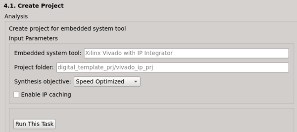
Figure 16 Build step 4.1 Synthesis objective speed optimized
The bootfile generated from this model does have some remaining timing violations within a MATLAB IP block. They do not significantly impact the performance of the system, however if they are desired to be removed, a custom set of blocks could be designed to replace the IP block.