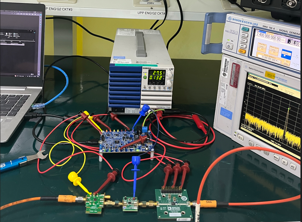
Primary Side
Power Supply Connectors
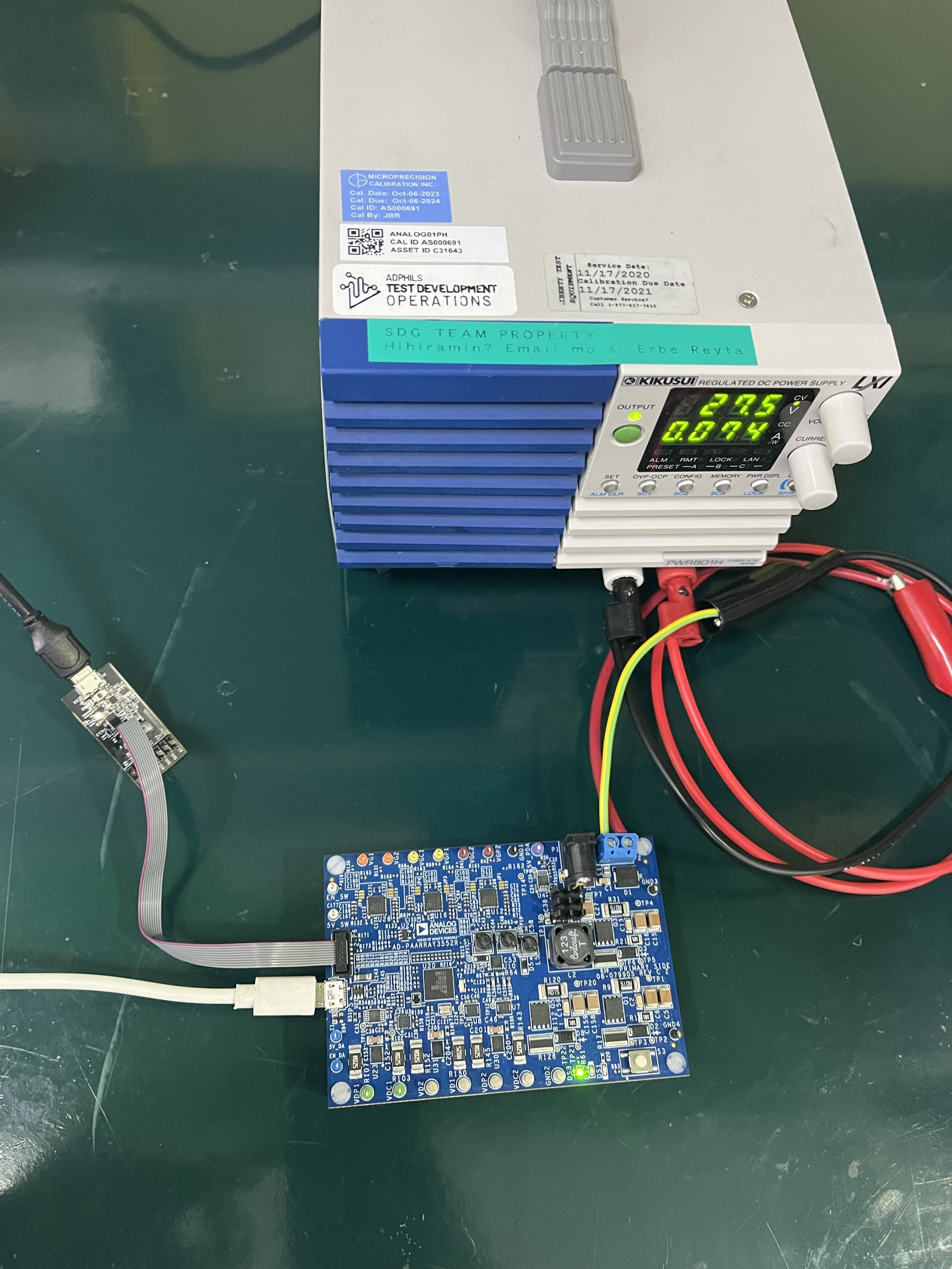
These connectors are used to supply +48V to the entire circuitry. The AD-PAARRAY3552R-SL provides an option for the user to use either a barrel jack connector or a two-wire terminal.
P1 - Barrel connector jack. Use this port if a 5.5 mm x 2.5 mm barrel jack adapter is preferred.
P2 - Two-port terminal connector. Port for supply power through non-terminated wires. Ensure proper connection to the positive and negative terminals of the power supply.
Important
Supply power to either P1 or P2 only and not at the same time Supplying power to both terminals may cause permanent damage to the device.
LED Indicators
Three indicator LEDs to display the board’s current status:
DS1 - Indicates that a fault event (overvoltage or overcurrent).
DS2 - Indicates that a fault event (overtemperature).
DS3 - Indicates normal operation and good power regulation.
Peripheral Connectors
These connectors are used for debugging, programming, and communication between the software and hardware.
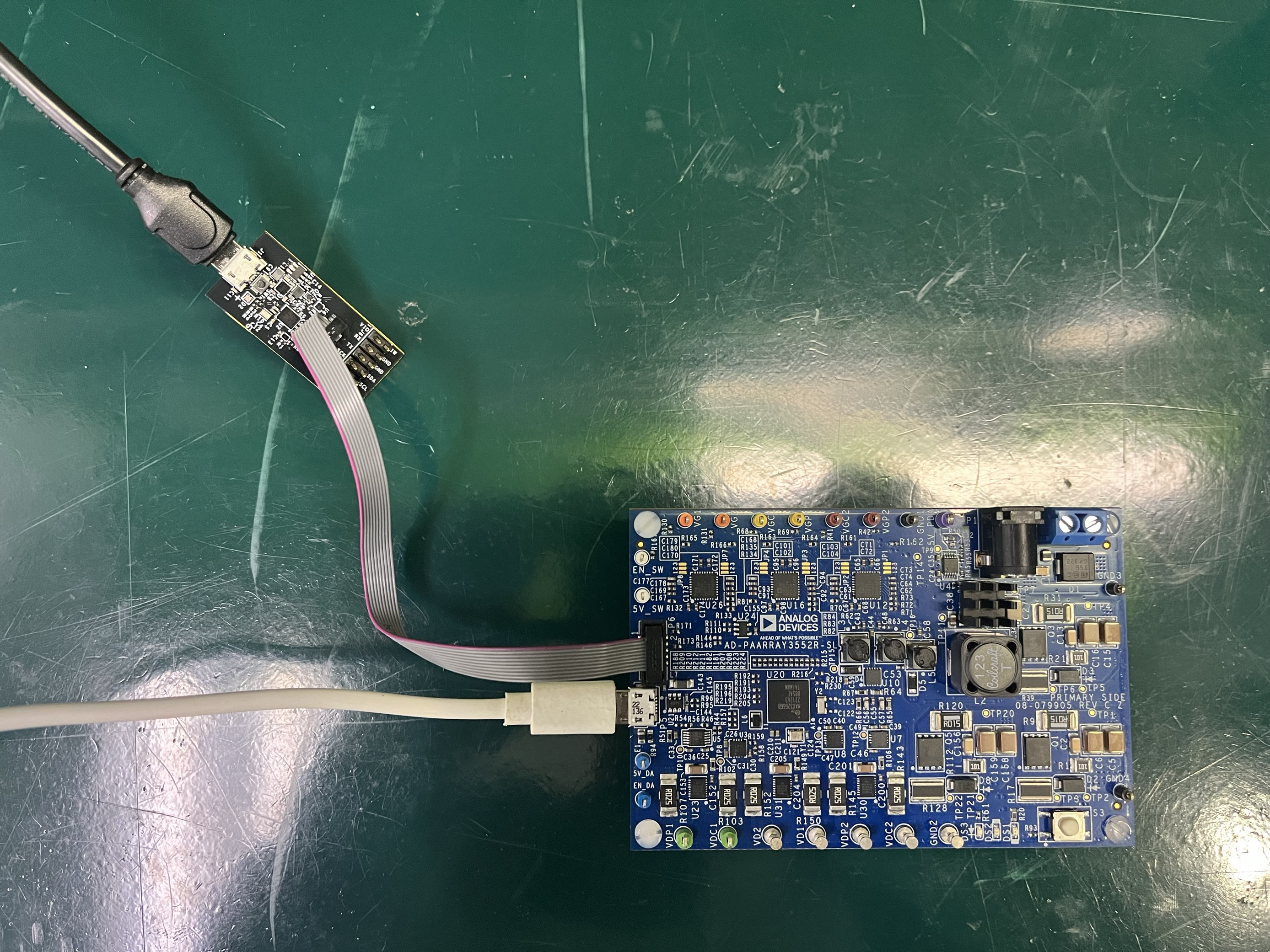
P5 - USB-to-UART Serial Communication through micro-USB to USB cable
P6 - Programming and debugging using 10-pin SWD cable
Switches
Hardware switches used to reset specific devices:
S3 - MAX32666 Microcontroller Reset
Test Points
The reference design board is comprised of several test points. The table below describes some of the most significant test points and their descriptions.
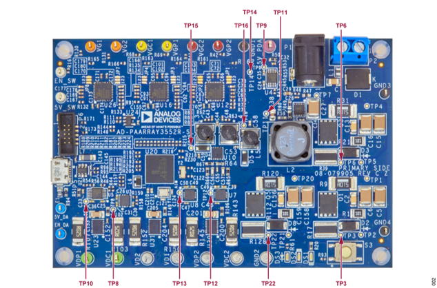
TP Name |
Description |
Voltage |
|---|---|---|
TP6 |
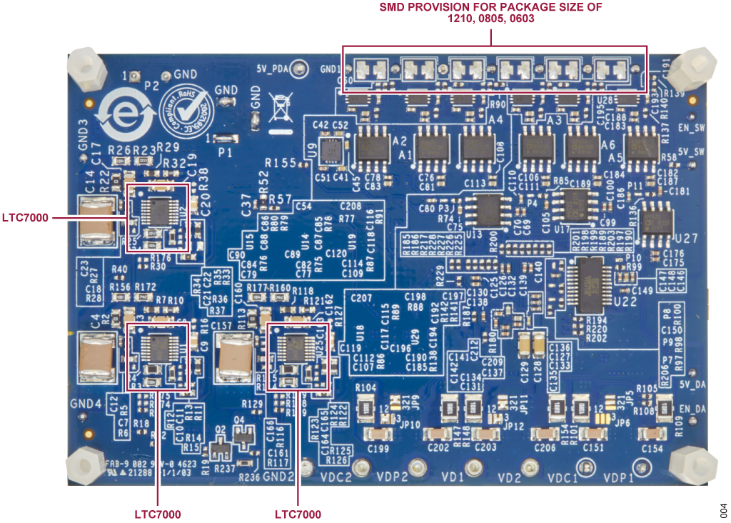
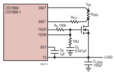
U2 LTC7000 Output |
+48V |
TP8 |
U3 ADM7172 LDO Output |
+5V |
TP9 |
U4 LT3042 LDO Output |
+5V |
TP10 |
U5 LT3042 LDO Output |
+5V |
TP11 |
U6 MAX17643 Output |
+5.6V |
TP12 |
U7 ADM7170 LDO Output |
+3.3V |
TP13 |
U8 ADM7170 LDO Output |
+1.8V |
TP14 |
U9 ADM7150 LDO Output |
+5V |
TP15 |
U10 LT3471 Positive Output |
+12V |
TP16 |
U10 LT3471 Negative Output |
-12V |
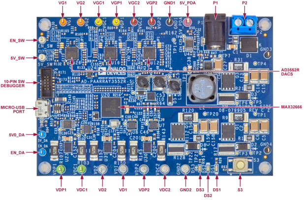
Pin Turrets and Hooks
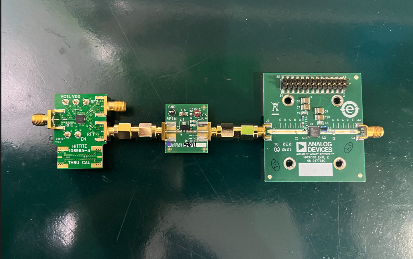
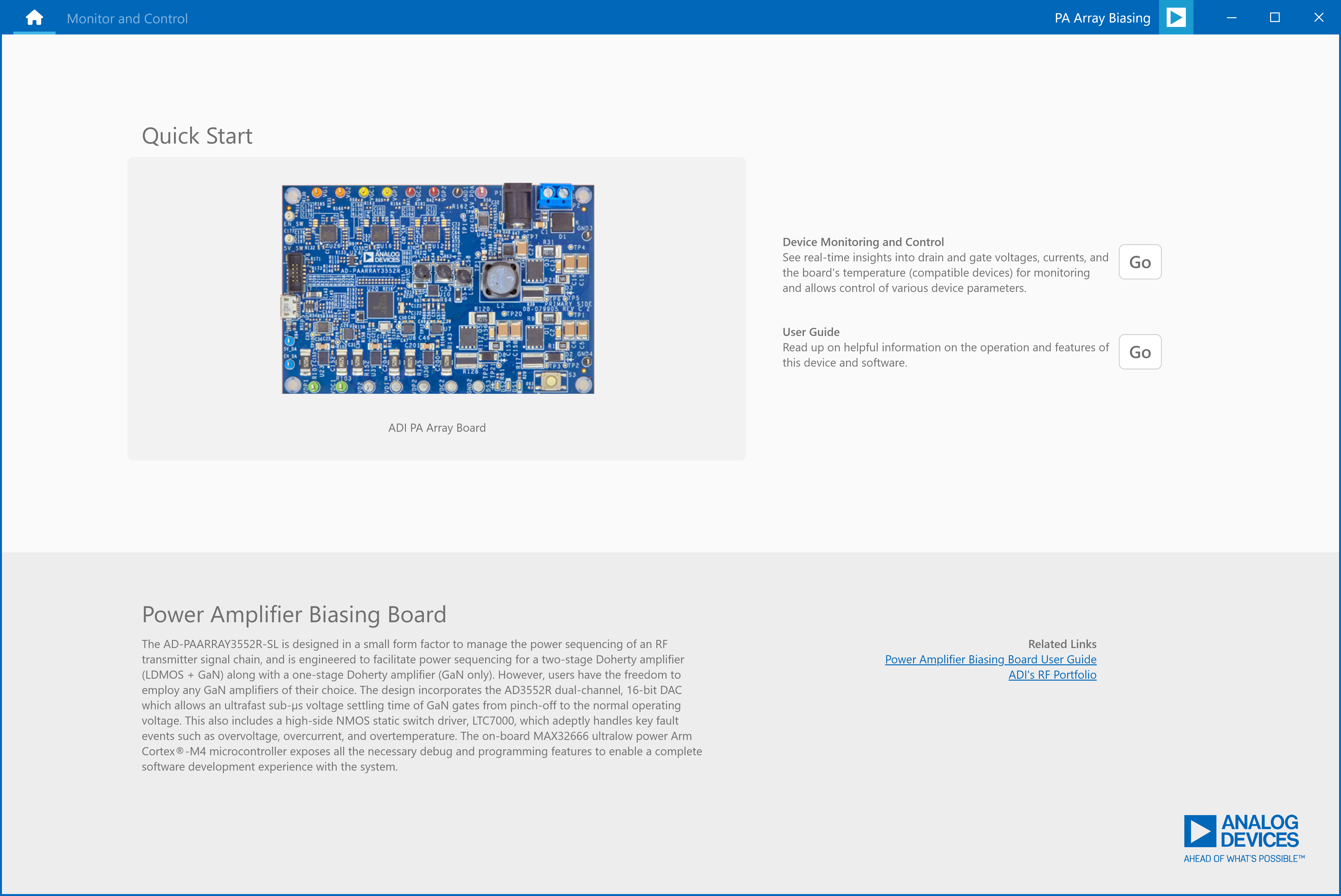
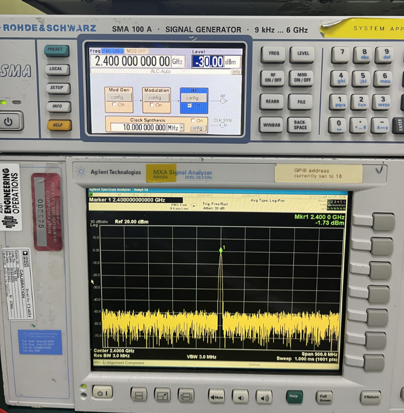
The AD-PAARRAY3552R-SL is designed for specific power amplifiers and is used on the RF signal chain, as shown below.

The bias lines of these amplifiers must be connected to the designated pinout on the reference design board. Refer to the table below for the correct pin assignments.
Pin Assignments |
||
|---|---|---|
Pin Name |
Description |
Pin Type |
5V0_SW |
RF Switch +5V Pin |
Hook |
EN_SW |
RF Switch Enable Pin |
Hook |
5V0_PDA |
Pre-driver Amplifier +5V Pin |
Hook |
5V0_DA |
Driver Amplifier +5V Pin |
Hook |
EN_DA |
Driver Amplifier Enable Pin |
Hook |
VDC1 |
Doherty LDMOS Carrier Drain Pin |
Hook |
VDP1 |
Doherty LDMOS Peaking Drain Pin |
Hook |
VGC1 |
Doherty LDMOS Carrier Gate Pin |
Hook |
VGP1 |
Doherty LDMOS Peaking Gate Pin |
Hook |
VDC2 |
Doherty GaN Carrier Drain Pin |
Turret |
VDP2 |
Doherty GaN Peaking Drain Pin |
Turret |
VGC2 |
Doherty GaN Carrier Gate Pin |
Hook |
VGP2 |
Doherty GaN Peaking Gate Pin |
Hook |
VD1 |
GaN Main Drain Pin |
Turret |
VD2 |
GaN Peak Drain Pin |
Turret |
VG1 |
GaN Main Gate Pin |
Hook |
VG2 |
GaN Peak Gate Pin |
Hook |