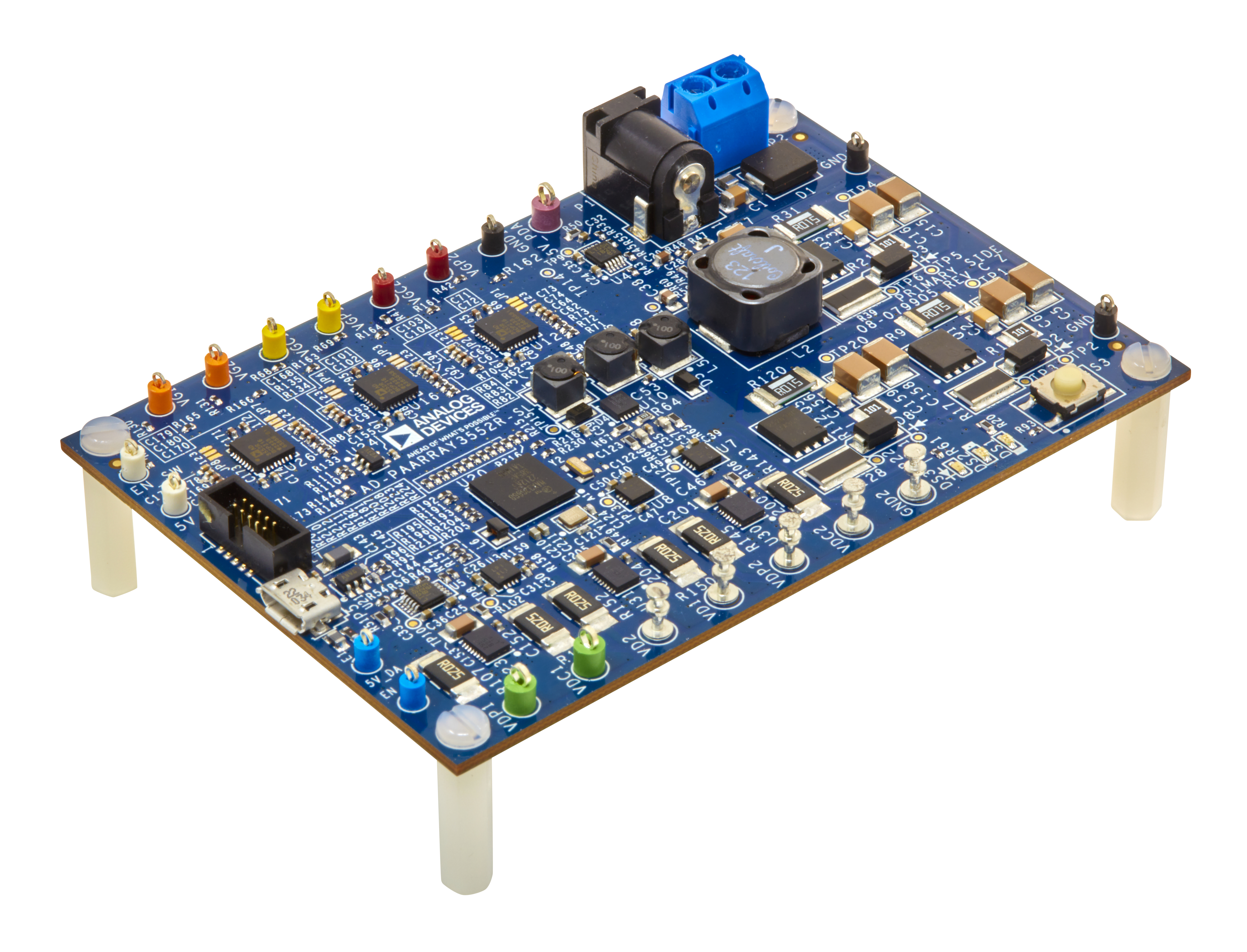
AD-PAARRAY3552R-SL
RF Front-end GaN Power Amplifier Biasing, Protection, and Control Reference Design.
Overview
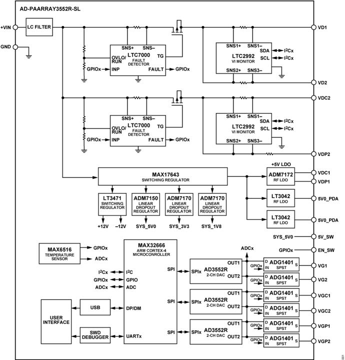
The AD-PAARRAY3552R-SL reference design provides biasing control and protection of Gallium Nitride (GaN) and Gallium Arsenide (GaAs) power amplifier (PA). Designed for massive multiple input - multiple output (MIMO) and macro base station RF front-end applications.
The system automatically manages the biasing sequence of GaN power amplifiers while continuously monitoring crucial parameters such voltages, currents, and temperatures.
The core of this solution is the AD3552R high-speed, dual-channel, 16-bit DAC, which supports ultrafast sub-µs voltage settling time of GaN gates.
It also features the LTC7000, a high-side NMOS static switch driver that adeptly handles key fault events such as overvoltage, overcurrent, and overtemperature.
The on-board MAX32666 ultralow power Arm Cortex-M4 microcontroller oversees the biasing sequence, sensor management, and user interface. The firmware can be effortlessly updated via SWD, UART-bootloader, facilitating rapid prototyping and development.
The AD-PAARRAY3552R-SL is a compact, user-friendly, microcontroller-controlled system designed to bias GaN PAs automatically and, to monitor the gate voltage, drain current, drain voltage, and transistor temperature.
Features
Designed to cover full Tx signal chains with integrated MCU and user-friendly GUI for faster and easier evaluation
Supports fault event protection: overvoltage (OV), overcurrent (OC), and overtemperature (OT)
Robust GaN/GaAs power amplifier biasing at any power-up/power-down sequence
Supports ultrafast sub-µs GaN gate voltage switching ~ (<1 µs)
Supports ultrafast fault event protection from detection up to gate pinch-off (<10 µs)
Wide range of gate bias voltages from -10 V to +10 V
Wide range of drain bias voltage from +38 V to +55 V (adjustable)
Configurable power-up and power-down sequence
Can accommodate from two to four GaN/GaAs Power Amplifiers
Real-time monitoring of voltages, currents, and temperature.
Applications
5G massive MIMOs
Macro base stations
Testing and Automation
System Architecture
Specifications
Features |
|
|---|---|
Drain Voltage Range |
+38 V to +55 V (can be adjusted from +4.5 V to +60 V) |
Gate Voltage Range |
-10 V to +10 V |
Drain Current |
40 A |
Gate Current |
±1.6 mA |
Gate Voltage Ripple |
2 mV (p-p) |
Rise Time |
738 ns (@10nF load) |
Fall Time |
< 1us (@10nF load) |
Fault Event |
|
Overvoltage |
+55 V (can be adjusted from +4.5 V to +55 V) |
Overcurrent |
3.5 A (can be adjusted from 1.3 A to 5 A) |
Overtemperature |
+75°C |
Computing Resources |
|
CPU |
MAX32666 Low-Power Arm Cortex-M4 with FPU-Based Microcontroller with Bluetooth 5 for Wearables |
Memory |
1 MB SRAM |
Storage |
64 MB QSPI Flash |
User Interface & Control |
|
Communication |
UART |
Debugging |
SWD |
Power Supply |
|
External |
+48 V DC with higher current capabilities |
Operating Conditions |
|
Operating temperature |
-45°C to +75°C |
Package Contents
1 x AD-PAARRAY3552R-SL board
4 x Standoffs
4 x Screws
The solution also comes with a pre-programmed firmware allowing the system to interface with a PC application for a system configuration, control, and data acquisition through serial interface.
To update the firmware on the on-board MCU, the user needs to purchase the MAX32625 PICO Evaluation Kit separately.
User Guides
Visit the AD-PAARRAY3552R-SL Software User Guide page to learn how to install the firmware and use the application GUI
For comprehensive details on hardware configuration, design files, and usage instructions for the AD-PAARRAY3552R-SL, refer to the AD-PAARRAY3552R-SL Hardware User Guide.
Further Help
For questions and more information about this product, connect with us through the Analog Devices Engineer Zone.