Hardware User Guide
Introduction
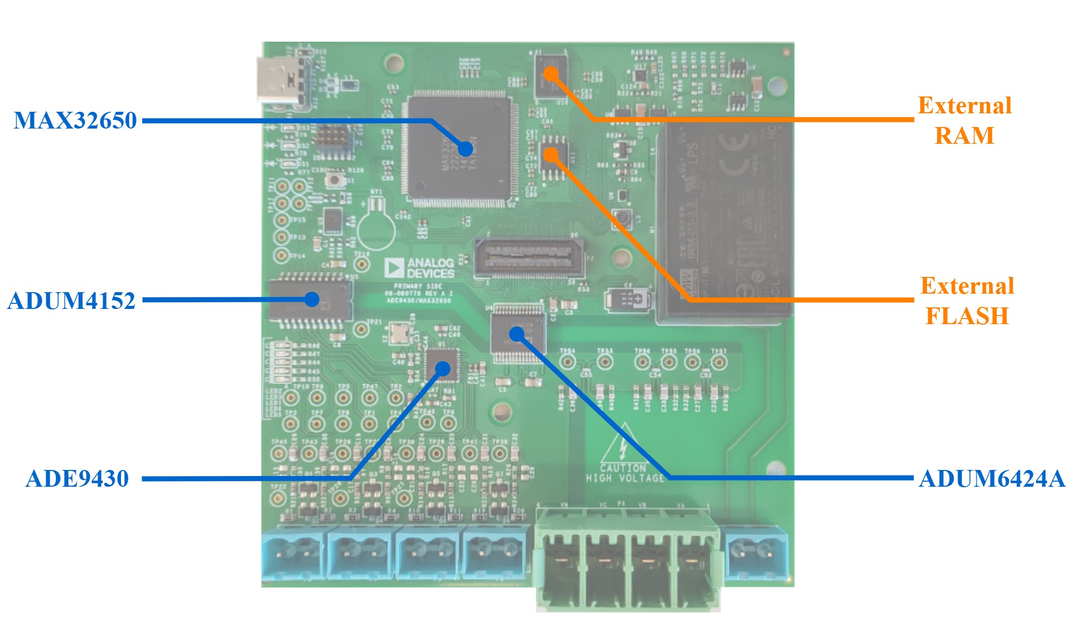
The AD-PQMON-SL provides a complete software and hardware platform for prototyping and evaluating high performance class S polyphase energy quality monitors. The design incorporates the ADE9430 high performance, polyphase energy monitoring IC that has an advanced metrology feature set (total and fundamental active power, volt amperes reactive (VAR), volt amperes (VA), watthour, VAR hour, VA hour, total and fundamental IRMS and VRMS, power factor) and the MAX32650 ultralow power ARM cortex-M4 with FPU-based microcontroller with 3 MB flash and 1 MB SRAM. The ADE9430 enables accurate energy monitoring over a wide dynamic range through its superior analog performance and digital signal processing (DSP) core. The ADE9430 simplifies the implementation and certification of energy and power quality monitoring systems by providing tight integration of acquisition and calculation engines. This solution can be used on a 3-phase system or up to three single-phase systems.
The design also features the MAX32650, which is a part of a new breed of low-power microcontrollers built to thrive in the rapidly evolving Internet of Things (IoT) named DARWIN. These MCUs are smart, with the biggest memories in their class and a massively scalable memory architecture. The MCU exposes all the necessary debug and programming features to enable a complete software development experience with the system. It is coupled with 512 Mb RAM and 64 Mb flash external memories to provide flexibility. The system’s firmware is based on ADI’s open-source no-OS framework and ADI proprietary ADSW-PQ-CLS library.
Front-end
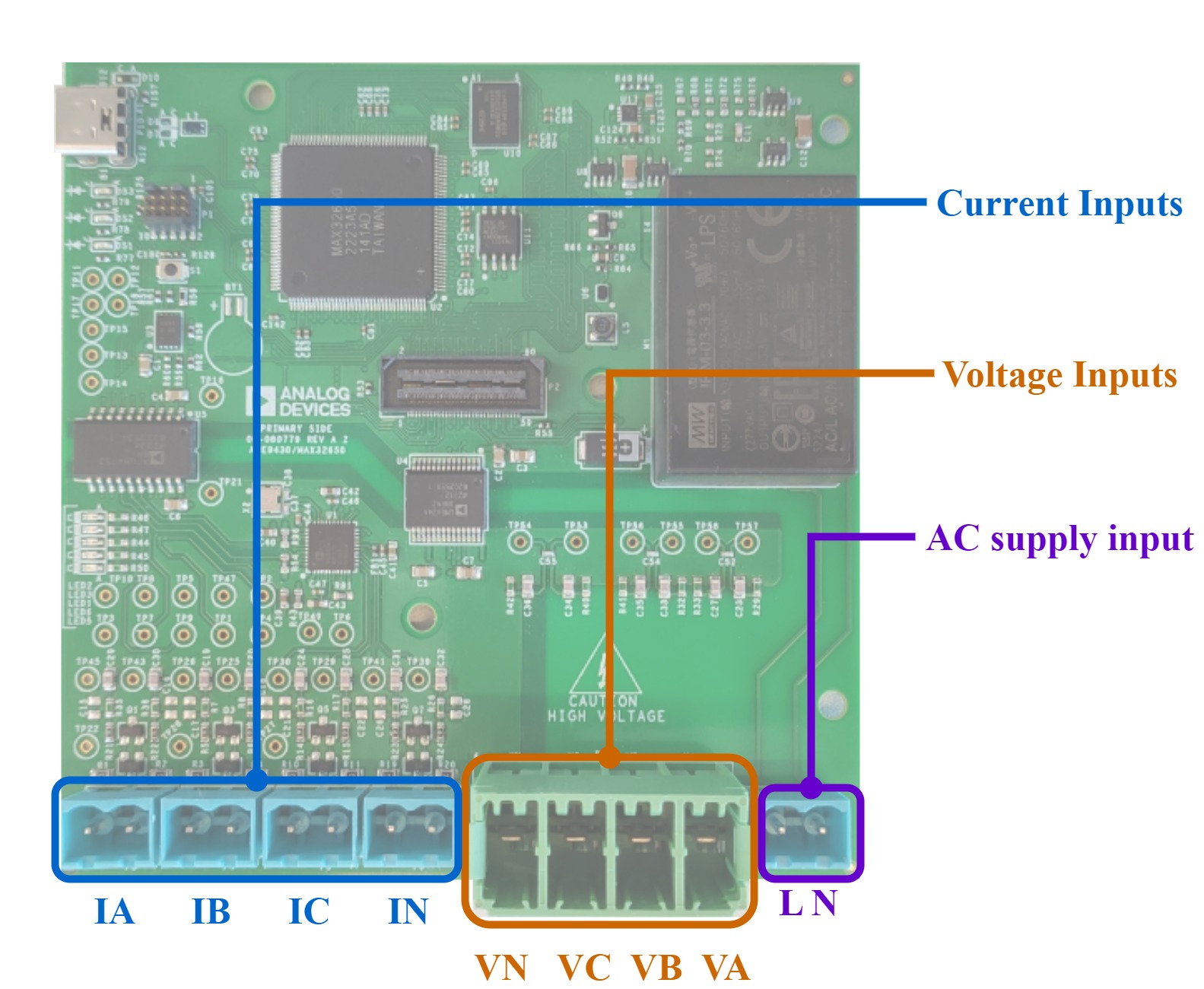
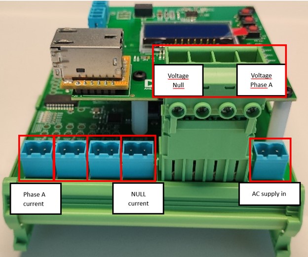
The AD-PQMON-SL uses all seven second order Σ-Δ ADCs of the ADE9430. There are 4 current inputs and 3 voltage ones that can be seen in the following image. The fourth voltage input is used for NULL if it is the case or it is connected to the reference phase, see ADE9430 user guide.
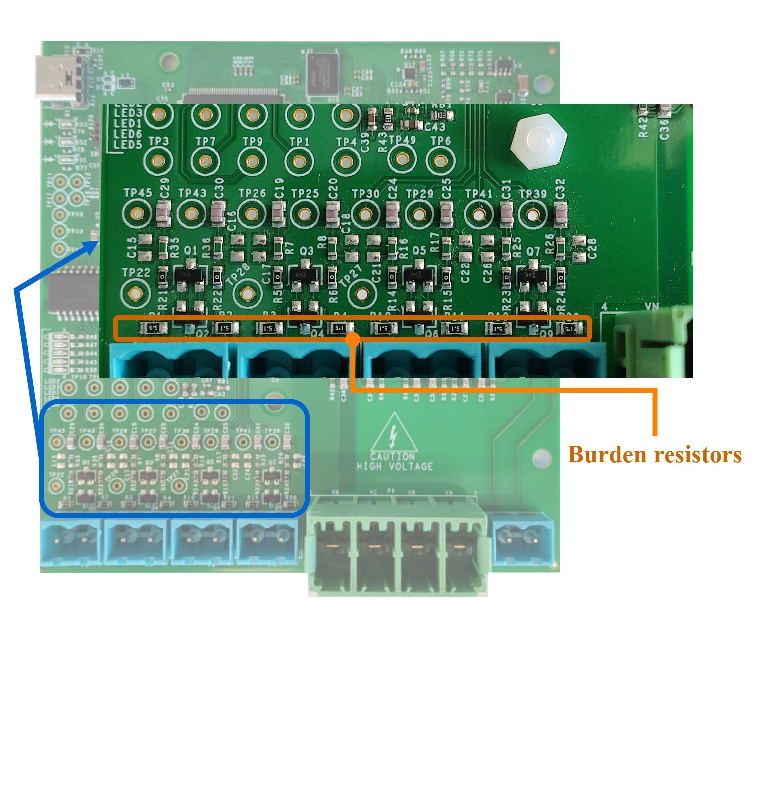
Current transformers (CT) for all four channels are provided with the kit. To connect the current transformers provided with the kit, the connectors of the current transformers must be replaced with the ones included in the box. The center tapped burden resistors are calculated for the provided CTs.
If one decides to change the CTs, these resistances need to be recalculated and replaced with the new values. The board is populated with 5.1 Ω resistances, resulting a current transfer function for a 3000:1 current transformer ratio equal with:
The current gain in this case will be 3000 / 10.2 = 294.11 (the default value in the firmware). If the burden resistances are changed the value of the current gain has to be updated from the Scopy interface.
For the voltage input the voltage gain is computed considering the upper resistance from the divider approximately 1 MΩ and the lower resistance equal with 1 kΩ resulting a value of 1001. The voltage transfer function is:
Power Supply
The board can be supplied from the AC input through an isolated AC/DC converter or from the USB through the LTC3306, a 1.75A Synchronous Step-Down Regulator. A logic based on several MAX40203, an Ultra-Tiny nanoPower, 1A Ideal Diodes with Ultralow-Voltage Drop, selects based on availability the supply input with priority to the AC input.
The other 1.1V and 1.8V voltage rails needed by the MCU are converted from the 3.3V input by the ADP225, a Dual, 300 mA Adjustable Output, Quick Output Discharge, Low Noise, High PSRR Voltage Regulator.
Isolation
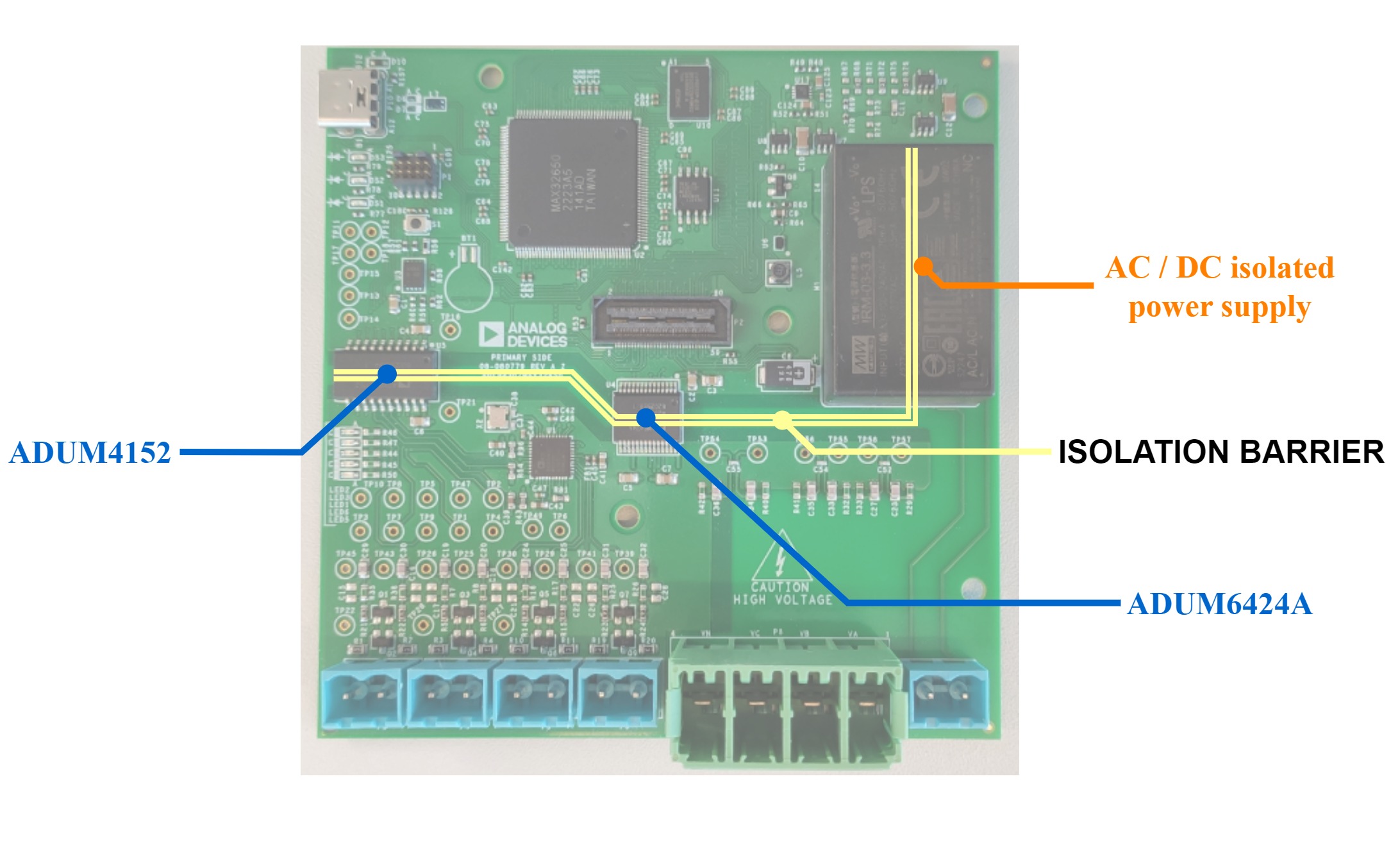
The solution has an on-board ADuM6424A Quad-Channel Isolator with Integrated DC-to-DC Converter. This DC-DC converter is used to supply all the components on the high voltage side. The ADUM6424A and the ADUM4152, which is a 5 kV, 7-Channel, SPIsolator™ Digital Isolator for SPI (with 1/2 Aux channel directionality), are used to isolate the connection between the ADE9430 and MAX32650.
In case the AC input is used to supply the board, the AC-DC flyback converter isolates the two sides.
LED Indicators
There are 8 LEDs on the PQMON motherboard. Five of them are on the ADE side and three on the isolated side.
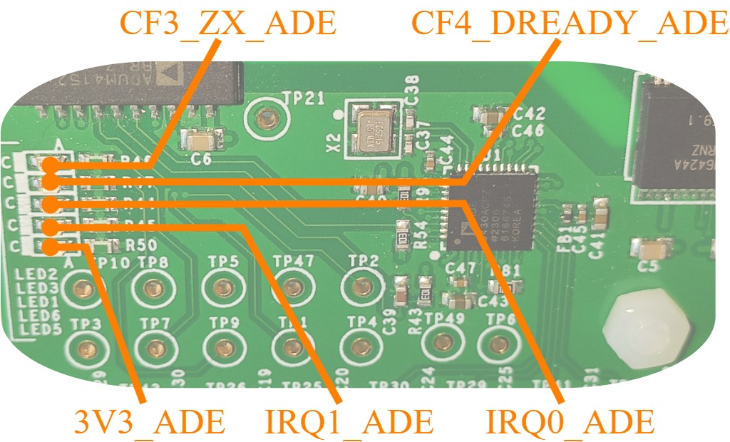
The five on the ADE side are connected as follows:
LED1 - IRQ0 ADE
LED2 - CF3/ZX ADE
LED3 - CF4/DREADY ADE
LED5 - 3V3 on the ADE side
LED5 - IRQ1 ADE
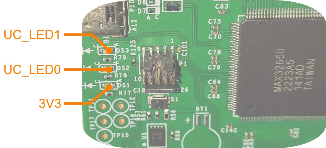
The three on the MCU side are connected as:
DS1 - 3V3 MCU side
DS2 - user led 0
DS3 - user led 1
Daughter Board Expansion
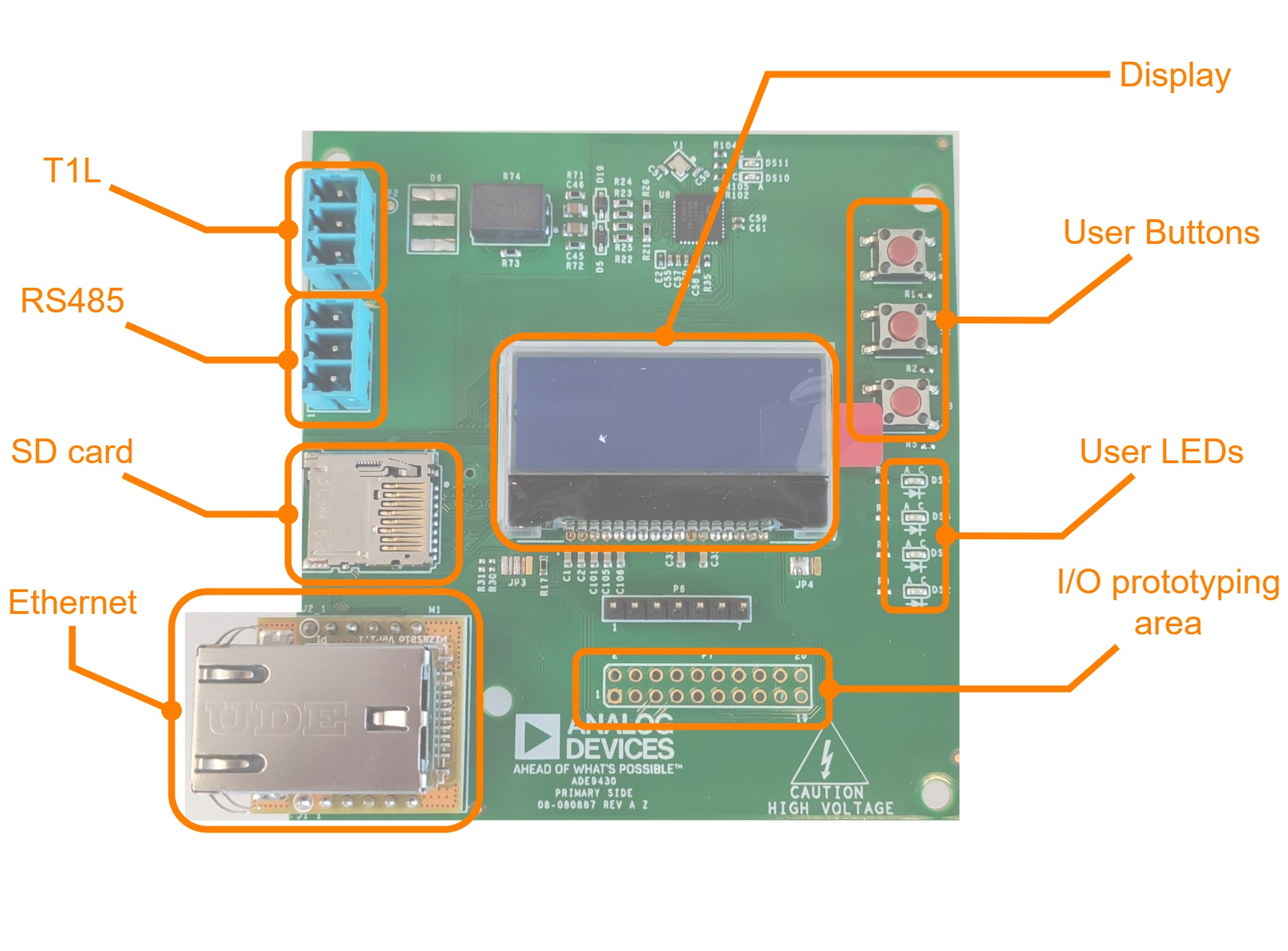
The add-on board includes a standalone interface (a 64 x 4 display, 2 LEDs, and 5 buttons), an SD card for long time data logging, several industrial connectivity ports, and exposes an I/O prototyping area for I2C, SPI, GPIO, UART, 3V3, GND. The prototyping area can be also used for GPS / GNSS (e.g., Accurate Synchrophasor Measurement) or for external control signals.
Conectivity Options
The following possibilities are available for industrial connectivity:
System Setup
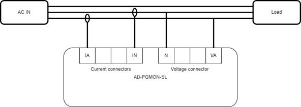
Single Phase Setup Example
For single phase testing, an example on how to connect the evaluation board can be seen in the following images:
A block schematic of the setup is provided in the following image.
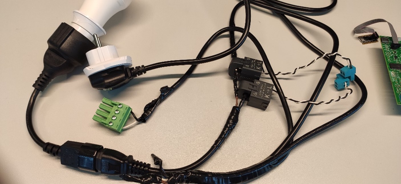
An example of a cable assembly that replicates the block schematic connections is presented in the following image. With this cable, tests can be made using different loads.
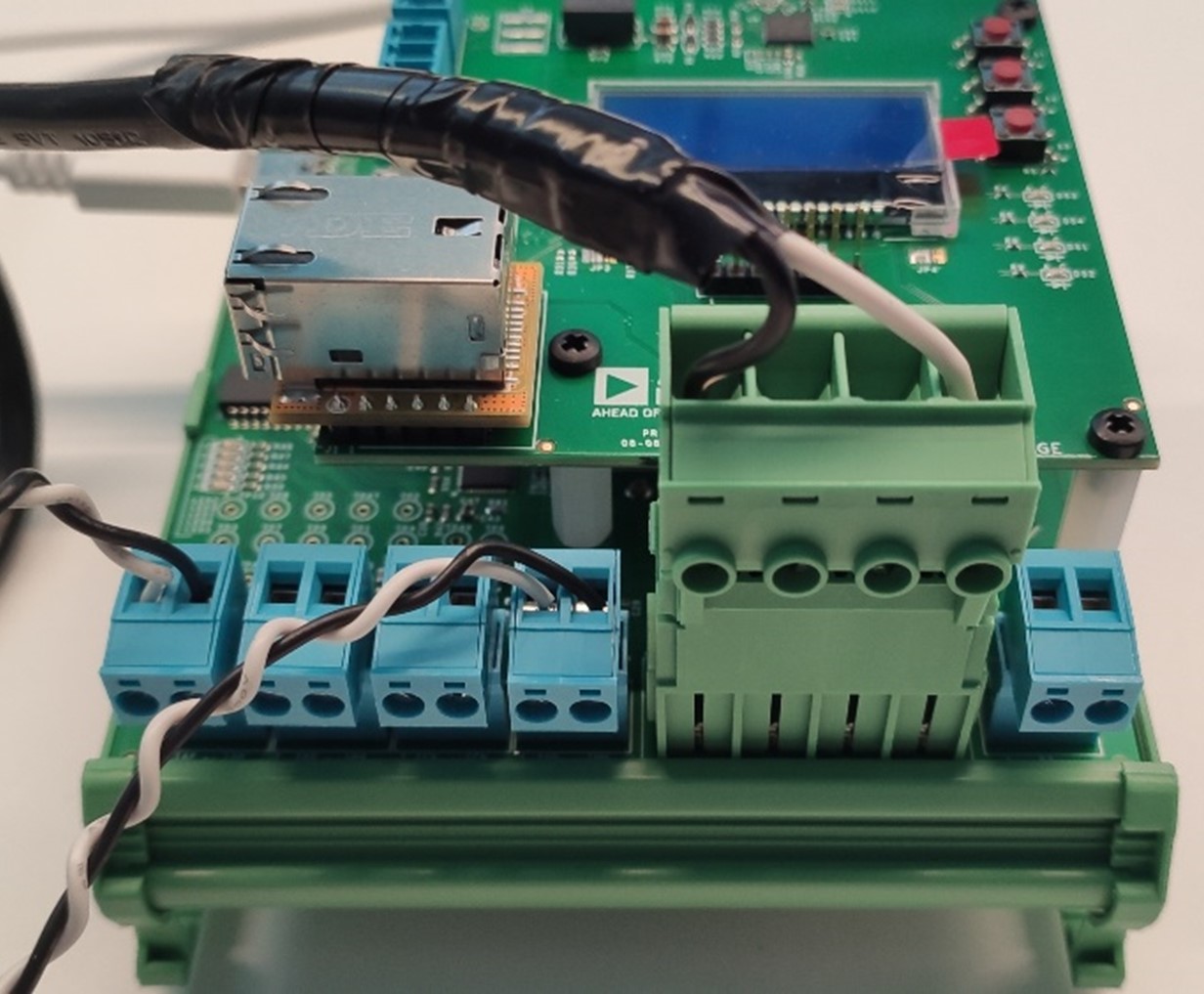
The cable is connected to the board as shown in the following image.
Setup for Testing All Channels Using a Single-Phase Input
For testing all the channels provided by the ADE9430, the following setup can be used.
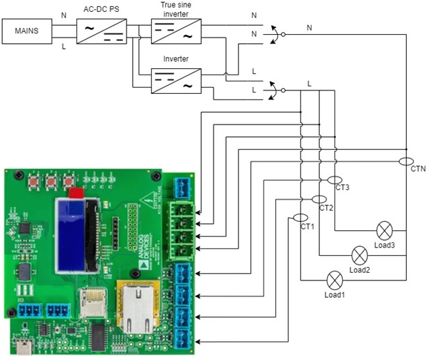
The mains voltage can also be connected to the load if a switch with more poles is used. With this setup one can observe the influence of the input power supply and of different types of loads on the power quality.
For 3-phase setups, consult the ADE9430 technical reference manual here.