AD-PS3803-RD
PoE+ with Ideal Diode Bridge to Isolated Flyback DC/DC (12V, 2A).
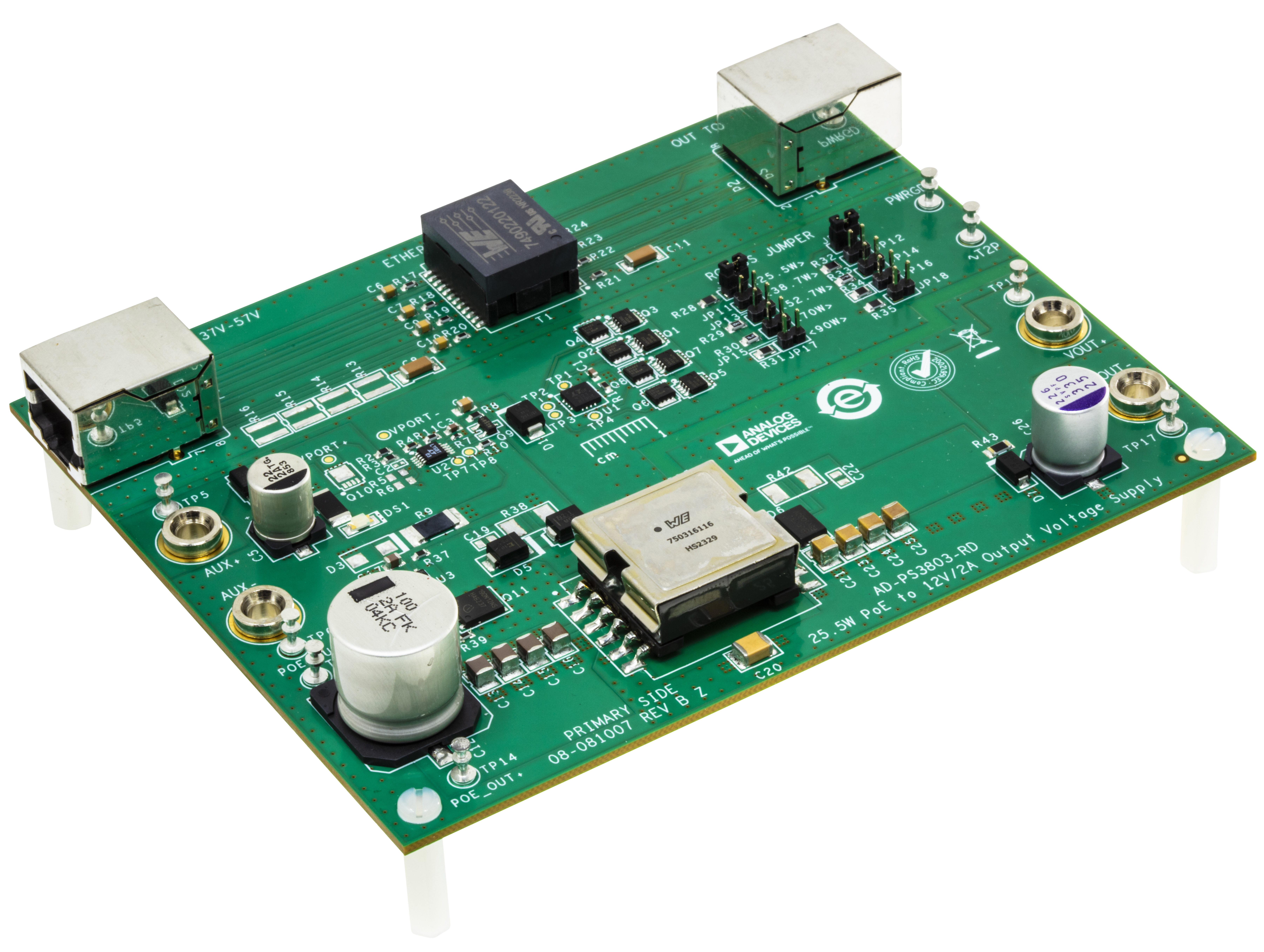
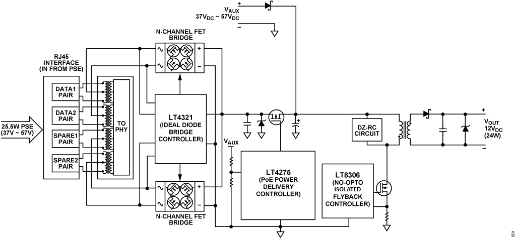
The AD-PS3803-RD reference design is a power converter capable of harnessing any IEEE802.3at (PoE+, Type 2) - compliant downstream power over Ethernet (PoE) supply to provide a galvanically isolated DC power.
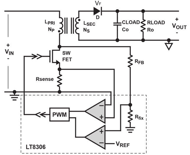
At the core of this solution is the LT8306 60V no-opto flyback controller, stepping down the 37V to 57V PoE input voltage to a 12V, 24W DC output.
The on-board LT4275 LTPoE++/PoE+/PoE power delivery (PD) controller handles interfacing and power delivery to any PoE supply.
The LT4321 ideal diode bridge controller is used for improved end-to-end power delivery efficiency and eased thermal design by utilizing low RDS(ON) N-Channel FETs, replacing the eight-diode configuration typically found in passive PoE rectifier bridge.
The AD-PS3803-RD also has auxiliary DC power support for a wide input range of 37V to 57V.
Features
Galvanically isolated 12 V flyback DC output with up to 24 W of output power capability
No transformer third winding or opto-isolator for output regulation
Supports multiple PoE power classes, interfacing and power supply control via a configurable jumper array:
IEEE802.3at & PoE+, (Type 2),
IEEE802.3bt & PoE++, (Type 3 and 4), re-design of isolated DC-DC converter is required, (see Higher Power Configuration section).
Supports a wide input DC auxiliary power of 37 V to 57 V
Applications
Industrial Automation
Surveillance Camera Systems
VoIP Phones
Payment Terminal Systems
Wireless Access Points
Block Diagram
Specifications
The following are the performance parameters of AD-PS3803-RD.
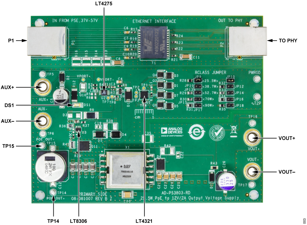
Components and Connections
Basic Input and Output Ports
Warning
Observe correct polarity for each port connection to prevent damaging the device.
Power Supply Ports
Power the board either through its RJ45 female connector (PoE input) or via its DC auxiliary terminals.
Both ports can handle input voltage of 37 VDC to 57 VDC.
P1 - RJ45 input port for PoE from PSE
AUX+ - Positive input terminal for auxiliary DC power supply
AUX- - Negative input terminal for auxiliary DC power supply
Output Ports
VOUT+ - Positive output terminal of the board
VOUT- - Negative output terminal of the board
TP14 - POE_OUT+ terminal. This is the positive terminal of the passthrough voltage from either the PoE input or the auxiliary input.
TP15 - POE_OUT- terminal. This is the positive terminal of the passthrough voltage from either the PoE input or the auxiliary input.
P2 - RJ45 output port for PHY
LED Indicators
DS1 - Indicator for successful PD and PSE handshaking. This should remain turned on during normal operation.
Test Points
Numerous test points such as turrets and test pads were added for easier probing of signals.
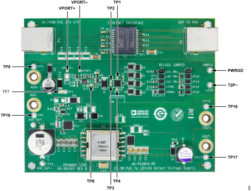
Ethernet Pairs
TP1 - DATA-1 wire pair test pad
TP2 - DATA-2 wire pair test pad
TP3 - SPARE-1 wire pair test pad
TP4 - SPARE-2 wire pair test pad
Accessory Test Points
TP5 - Turret for AUX+ terminal
TP6 - Turret for AUX- terminal
TP7 - Test pad for T2P~
TP8 - Test pad for PWRGD
VPORT+ - Test pad for the positive terminal of the rectified voltage after the ideal diode bridge
VPORT- - Test pad for the negative terminal of the rectified voltage after the ideal diode bridge
PWRGD - Power good indicator. This terminal is pulled high when negotiation with PSE is established and power is available. Logic level is equal to voltage at POE_OUT+ terminal with respect to POE_OUT-.
T2P~ - PSE type indicator. Pulled down when a IEEE802.3at (PoE+, Type 2) compliant PSE is connected. A square wave with 50% duty cycle can be read when a LTPoE+.+ compliant PSE is detected.
TP16 - Turret for VOUT+ terminal
TP17 - Turret for VOUT- terminal
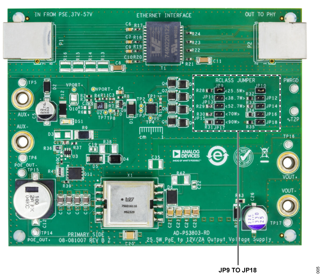
Class Select Jumpers
The board’s operating power level can be configured by changing the position of the class select jumpers, allowing different PSEs to be compatible with the device.
Circuit Evaluation
AD-PS3803-RD Quick Start Procedure
Power over Ethernet using a Power Sourcing Equipment (PSE)
Figures 6 and 7 show the setup for evaluating the AD-PS3803-RD using a PSE. A resistive load or an active load can be used at the output stage of the device.
Tip
Default class select shunt positions are at JP9 and JP10 on the AD-PS3803-RD board.
With this configuration, any PSE with sufficient power will turn on the board. Refer to Table 2 for the shunt positions in selecting a different power level.
Check the power delivery capacity of the PSE, ensure that it can provide the required power and load.
Important
Avoid selecting a jumper configuration corresponding to a higher power level than the PSE can provide. Otherwise, the PSE will not turn on the board after its classification stage.
Connect the output of the PSE to the RJ45 connector (P1) on the AD-PS3803-RD board using a CAT5e or CAT6 Ethernet cable.
After connection has been established, verify that the LED (DS1) is on. This indicates successful handshaking between the PSE and AD-PS3803-RD.
Check for the proper output voltages. The output at the VOUT+ and VOUT- ports should be regulated at 12 V (±5%).
Once the proper output voltage is established, connect the load at the VOUT+ and VOUT- ports of the AD-PS3803-RD, observing proper polarity of the terminals.
Adjust the load current within the operating range and observe the output voltage regulation, ripple voltage, and other parameters.
Note
The AD-PS3803-RD requires a very small minimum load to maintain good output voltage regulation. A Zener diode is placed on the output to clamp the voltage to 13V at no load.
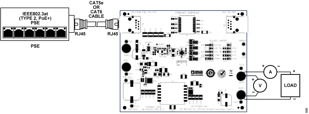
Figure 6 AD-PS3803-RD Setup with a Power Sourcing Equipment (PSE)
Auxiliary Power Supply
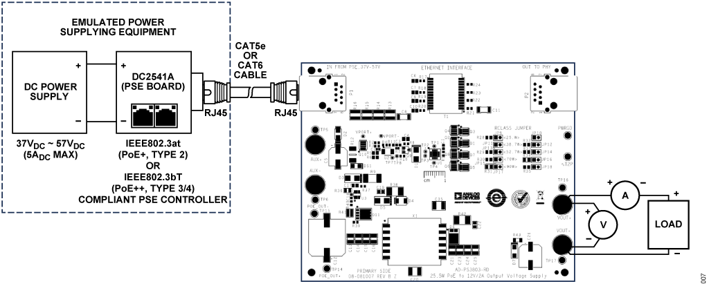
Refer to Figure 9 for evaluating the AD-PS3803-RD using an auxiliary power supply. A resistive load or an active load can be used at the output stage of the device.
Connect the auxiliary supply to the AUX+ to AUX- inputs. Observe proper polarity of voltage connection before turning on the auxiliary power supply.
Turn on the auxiliary power supply and verify that the LED (DS1) is on.
Check for the proper output voltages. The output at the VOUT+ and VOUT- ports should be regulated at 12 V (±5%).
Once the proper output voltage is established, connect the load at the VOUT+ and VOUT- ports of the AD-PS3803-RD as illustrated in Figure 9.
Warning
Observe correct polarity of connections to prevent damaging the device.
Figure 9 AD-PS3803-RD Test Setup using an Auxiliary Power Supply
Demo Setup
Equipment Needed
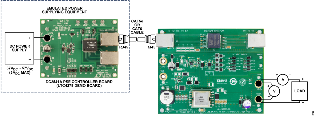
One (1) Programmable DC power supply capable of 60V/3A (DC power supply)
One (1) DC2541A PSE controller board (PSE)
One (1) RJ45-to-RJ45 Ethernet cable
One (1) Digital multimeter (Voltmeter #1)
One (1) Electronic load capable of 12V/2A (DC electronic load)
Getting Started
Note
The setup described below uses the DC2541A Demo Board as PSE Controller. Other PSE boards can also be used as alternative, but ensure that the interface and power range is compatible with the AD-PS3803-RD.
Before connecting any power supplies, adjust the DC power supply’s output to 0V and set the current limit to 0.1A.
Turn the supply OFF.
Connect all the equipment, as shown in Figure 10. Do NOT connect the Ethernet cable to AD-PS3803-RD yet.
Verify that the electronic load is initially at the OFF position.
Ensure that the indicated jumper position for DC2541A is set correctly, as shown in Table 3 and Figure 11.
PSE Type |
Power Mode (JP6) |
PORT+ (JP1) / PORT-(JP2) |
MID (JP3) |
DUALPD (JP4) |
LEGACY (JP5) |
IEEE 802.3at Type 2 (25.5W) |
Type 2 (25.5W) |
2-PAIR |
LO/HI |
LO |
LO |
Test Measurement
Turn the DC power supply ON and set the voltage to approximately 48V.
Set the DC power supply current limit to 1A.
Connect the RJ45-to-RJ45 Ethernet cable to AD-PS3803-RD, as illustrated in Figure 10.
Turn ON the DC electronic load and carefully set the current to 2A only.
Check the output voltage reading from Voltmeter #1 and verify that it is within the maximum and minimum limits, as indicated in Table 4.
Device under Test |
Minimum VOUT (V) |
Maximum VOUT (V) |
AD-PS3803-RD |
11.76 V |
12.24 V |
Set the DC power supply voltage to approximately 57V.
Verify that the DC electronic load is still set to the current of 2A.
Check the output voltage reading from Voltmeter #1 and verify that it is within the maximum and minimum limits as indicated in Table 4.
Set the DC electronic load to 0A.
Disconnect the RJ45-to-RJ45 Ethernet cable from AD-PS3803-RD.
System Performance
Efficiency
Below figure shows the efficiency performance of AD-PS3803-RD at PoE input voltage of 48V and 57V.

Figure 13 AD-PS3803-RD Efficiency vs. Load Current Performance
Output Regulation
The AD-PS3803-RD maintains within ±5% across its entire output current capability.
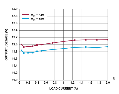
Figure 14 AD-PS3803-RD: Output Voltage vs. Load Current Performance
Higher Power Configuration
Configuring the PD Circuit at Higher Power Class
For enabling the PD circuit to receive the appropriate higher power classes from the PSE, AD-PS3803-RD must be modified as such, from configuring the power class selection of the PD controller, and the redesign of critical parts for higher power.
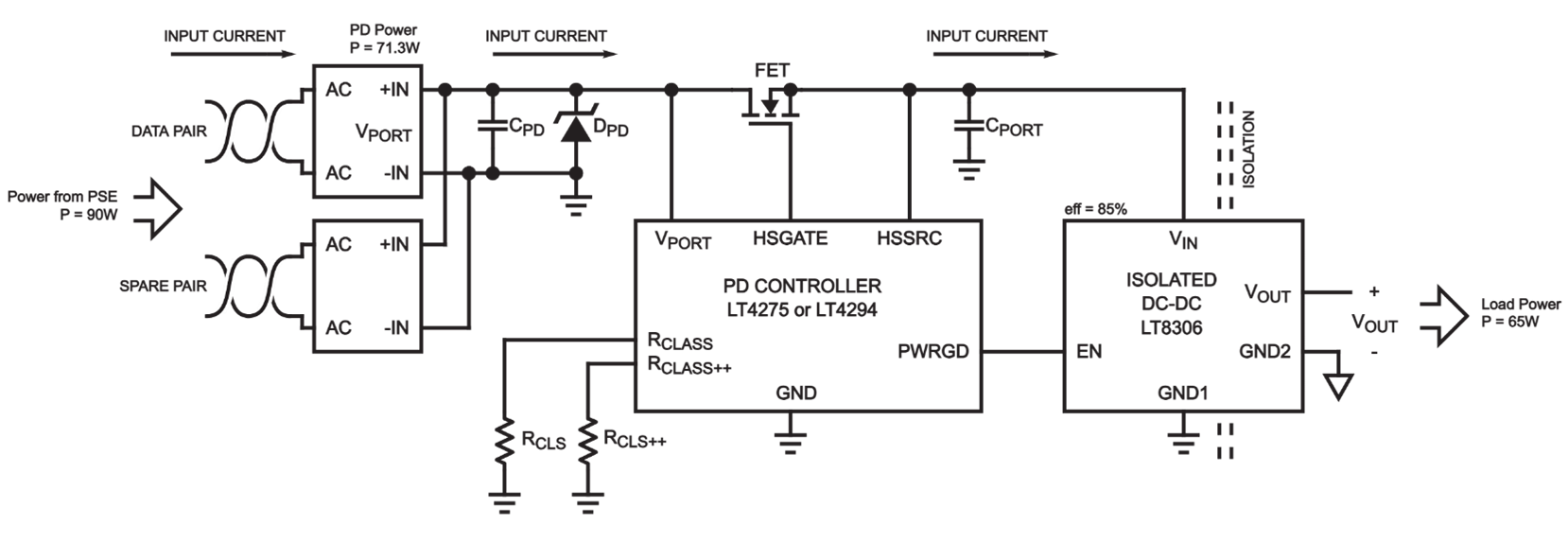
Figure 15 Simplified PD Controller Circuit with Isolated Supply
The hot-plug or inrush protection FET selected must be capable of higher parameters if it operates at higher power class, specifically the current that will flow from its drain to source IDS, which is the same input current of the PoE main line that may fluctuate as worst case to the peak current of the primary winding of the transformer IPRI. Improper selection of FET will cause overcurrent or failure of the FET.
Calculation
For Higher Current FET selection, it must satisfy Equation (1):
PD Controller Considerations
To make sure the PD controller is connected to the PSE, and that the PSE delivers the compatible power class, the power class resistor configuration should be set to the appropriate power delivery. If using the reference design AD-PS3803-RD, the same accessible jumper circuit can be used to select the power class. If designing on a new board, the correct resistor values for RCLS and RCLS++ must be applied, indicated on Table 6.
Technically the LTPoE++ proprietary specs of LT4275 can work on the IEEE802.3bt when set at higher power class, like 90W for 71.3W for example, but the user may want a PD controller part that will negotiate on the specific power class indicated by the IEEE 802.3, because the class naming and PD power are not entirely the same. In which the user can replace it with LT4294 PD controller specifically compliant to IEEE 802.3 PoE standards.
The LT4294 is pin compatible with LT4275, use Table 7 for the appropriate power class and resistor configuration of LT4294. Take note of the slight differences in the PD power and resistor values.
An LTPoE++ PD will be classified as class 4 by an IEEE 802.3 compliant PSE
Flyback Converter at Higher Power
The isolated DC-DC converter must be re-designed in the appropriate power delivery of the PoE circuit. For the flyback converter using the LT8306, the power class requirement will dictate the input power of the flyback and its entire design, especially the flyback transformer.
The flyback converter of the 25.5W power class is differently designed to the flyback converter of higher power like the 71.3W power class of IEEE 802.3bt.
Flyback Transformer Considerations
The flyback converter of AD-PS3803-RD is optimally designed for the 25.5W power class which reflects as the input power. This flyback will output a maximum power of 24W when efficiency and power loss are considered, translated to the output of 12V and 2A maximum as stated by the board’s specifications.
For higher power classes like the 70W of Class 4 LTPoE++ and 71.3W of Type 4 Class 8 IEEE802.3bt, a likely larger transformer with higher specification is required. The flyback circuit is designed only for 25.5W which is expected will not work on higher power class because it can make the transformer saturate, resulting in the DC-DC converter regulation collapsing.
We can verify this by checking the peak current of the primary winding of the transformer IPRI if it hits the transformer saturation specified on table 8, using equation 3 where input power is the PD power class, by first calculating switching frequency using equation 2.
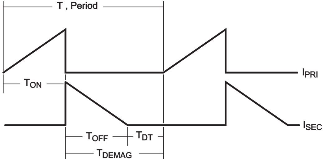
Figure 17 Transformer Primary Winding and Secondary Winding Currents
The switching frequency is dictated by the PWM controller of the flyback, which is LT8306. The on-time is the duration in which the current in the primary winding is conducting up to its peak, until it demagnetizes at the off-time where the secondary winding current conducts. If the flyback is operating at discontinuous conduction, there will be a dead-time in which both windings are not conducting. The cycle is complete after a time period of the primary winding conducting (on-time) and then the time demagnetizing, which dictates the switching frequency.
The switching frequency boundaries, along with the minimum on-time is limited and spec by the controller, in which the parameters are indicated by the LT8306 datasheet. The switching frequency is an important parameter for calculating primary winding peak current and power capability of the flyback converter when choosing or selecting the appropriate transformer.
For higher current capability, we can set LT8306’s limit current ILIM to 10A for example, just that the inductor peak current can go high enough for intended higher power.
Calculation
Switching Frequency is calculated by Equation (2):
Using the specs of 750316116, Switching frequency is 95.47 kHz
With the switching frequency calculated, the user can check if the selected transformer is applicable to the IEEE 802.3bt high input power of 71.3W by calculating the primary winding peak current IPRI, using equation 3.
Calculation
Flyback input power is presented by Equation (3):
Given that the PD input power for IEEE 802.3bt is 71.3W, then IPRI can be calculated:
For a peak current of 9.13A, unfortunately it exceeds the saturation of the transformer of 7.7A.
Another method of checking the capability of the transformer is the full-load output current it can deliver by using equation 4 and equation 5.
Calculation
Duty Cycle is calculated by Equation (4):
Output Current IOUT is calculated by Equation (5):
Assuming efficiency is 85%, we selected the previously calculated peak current of IPRI of 9.31A:
Calculation
Duty Cycle is around 30.1%:
Calculated IOUT is 4.75A, which is less then 5.4A output for PD of 71.3W:
If the designer wants to deliver the output power of 65W, for an input power of 71.3W when approximated efficiency of 85% is considered, the flyback must be able to deliver current of 5.4A at full load for an output voltage of 12V. The flyback in AD-PS3803-RD unfortunately is not designed for this, as it is only capable of delivering up to 4.75A at maximum, and it is not even optimized for that, because it is intentionally designed for 2A output (24W).
Therefore, the designer must select a new transformer that will not saturate at higher PoE power class, either picking a transformer with higher saturation current, or higher primary winding inductance, appropriate turns ratio, or at least it indicates that it can produce the maximum output current and output power if the saturation current specification is not available.
One example of a transformer that has a higher specification is 750319036 from Wurth Elektroniks. It is spec for power of up to 72W (12V at 6A).
Parameter |
Value |
Primary Winding Inductance LPRI |
16 µH |
Turns Ratio NPS |
2.33 |
Saturation Current ISAT |
10.4 A |
Primary Winding Resistance DCRPRI |
26.2 mΩ |
Using this transformer, we are calculating the switching frequency and primary winding peak current of 750319036 for 71.3W, setting ILIM = 10A again to make sure it does not violate the minimum switching frequency of 12.5kHz and to allow higher current ceiling like the previous calculation, which must be adequate on the given transformer inductance.
Calculation
For primary winding inductance of 16µH, FSW is more than 12.5kHz minimum.
Calculating the peak current again for the transfomer if it is capable for IEEE 802.3bt.
With the primary current known at IPRI = 8.65A, this proves that the transformer will not saturate, then we verify the duty cycle and see how much output or load current it can deliver.
Calculation
The duty cycle is around 33.46%.
IOUT is 5.7A, which is more than 5.4A.
The calculated IOUT = 5.7A proves that the output capability is within the maximum load that the flyback converter can deliver, so that the DC-DC supply can pull an input power of what is specified on the PoE power classes of 71.3W or 70W for the full load current of 5.4A (65W output).
The next checking will be the other parameters of the transformer, to ensure we select the compatible transformer for LT8306 flyback controller in terms of primary winding inductance and turns ratio using equations 6, 7 and 8.
Calculation
Sense Resistor for limiting current is Equation (6):
Maximum allowable turns-ratio is Equation (7):
Minimum inductance for primary winding of transformer is Equation (8):
Calculating other parameters using input conditions given by the LT8306 datasheet,
Where DMAX = 0.65, VSENSE(MIN) = 17mV, & TON(MIN) = 200ns.
Calculation
For a current limit of 10A, the sense resistor value must be 9.5mΩ.
The transformer’s turns ratio of 2.33 did not exceeed the calculated maximum turns ratio:
The inductance of the transformer is 16µH, which is more than the minimum inductance:
Therefore, the selected transformer 750319036 from Wurth Elektroniks is a recommended part for higher power flyback circuit for the application of higher power PoE up to 72W. Other alternative transformers are indicated in Table 10.
After the transformer consideration is to design the rest of the flyback circuit like the flyback diode, snubber circuit selection and output capacitor calculations. These are all straight forward and can be directly calculated with the equations provided by the LT8306 datasheet for this specific flyback circuit that being used on AD-PS3803-RD.
Warning
Important disclaimer that, for any isolated DC-DC converters, higher power delivery consequently means part selections are bigger and with different footprints, especially for the flyback transformer as its critical part.
The AD-PS3803-RD is optimally designed for 25.5W input power, so at higher power applications, the selected new transformer will not fit the footprint and pin assignment of the existing flyback transformer in the reference design. This is also an argument for the capacitor and diode selection. The diodes may not also fit its footprint due to larger size at higher current. Capacitances are usually high at higher current because of the ripple requirements of flyback, so it will require many capacitors. Therefore, the changes for higher PD power class will may not fit to the PCB of AD-PS3803-RD.
Here is an example part list of critical components on the flyback converter required for 71.3W input power, based on the simplified flyback circuit of figure 16.
Resources
Design & Integration Files
Download
AD-PS3803-RD Design & Integration Files
Schematic
PCB Layout
Bill of Materials
Allegro Project
LTspice Simulation
Help and Support
For questions and more information, please visit the Analog Devices Engineer Zone.