Versal Adaptive SoC Transceiver Subsystem
The Versal Transceiver Subsystem can be used to configure the GTY and GTYP for Versal ACAP devices. In general, across all reference designs, the gigabit transceivers are configured specifically to the Lane rate of the HDL build. This guide provides instructions on using the wizard to generate a transceiver configuration for JESD204B/C interfaces on Versal devices.
Note
To learn more about Versal ACAP transceivers and the Wizard, please consult:
Versal ACAP Transceiver Architecture
Versal ACAP devices feature advanced GTY and GTYP transceivers that support:
Lane rates from 1.2 Gb/s up to 28.21 Gb/s (GTY) and 32.0 Gb/s (GTYP)
Multiple PLL options: LCPLL and RPLL for flexible clocking
Enhanced performance and power efficiency compared to UltraScale+
Native JESD204B and JESD204C protocol support
Required features by the JESD204B
The following features are required for a JESD204B interface:
LCPLL for clock generation
8B/10B encoding and decoding
TX and RX buffer to solve rate and phase differences between XCLK (PMA parallel clock) and USRCLK (link clock)
RX Equalization and CDR
RX Byte and Word alignment
Required features by the JESD204C
The following features are required for a JESD204C interface:
LCPLL for clock generation
64B/66B async encoding and decoding
TX and RX buffer to solve rate and phase differences between XCLK (PMA parallel clock) and USRCLK (link clock)
RX Equalization and CDR
Lane Rate and RefClk Selection
In our reference designs, we usually use the following relationship between the Lane rate and the reference clock:
For JESD204B: Reference clock = Lane Rate / 40
For JESD204C: Reference clock = Lane Rate / 66
Versal Adaptive SoC Transceiver Subsystem wrapper
In our reference designs, we use a versal_xcvr_subsystem.tcl as a wrapper to instantiate and configure the Versal Transceiver Subsystem IP core.
The script takes the following parameters:
ip_name - Name of the IP core instance
jesd_mode:
8b10b - JESD204B
64b66b - JESD204C
rx_no_lanes - Number of RX lanes
tx_no_lanes - Number of TX lanes
rx_lane_rate - RX lane rate in Gb/s
tx_lane_rate - TX lane rate in Gb/s
ref_clock - Reference clock frequency in MHz (see Lane Rate and RefClk Selection)
transceiver - GTY or GTYP
intf_cfg:
RX - Simplex RX
TX - Simplex TX
RXTX - Simplex RX + Simplex TX
Versal Adaptive SoC Transceiver Subsystem to JESD204B/C Link Transmit Peripheral adapter
In order to connect the Versal Transceiver Subsystem to the JESD204B/C Link Transmit Peripheral, we provide a Link-to-Phy adapter.
This adapter is needed to convert the 64B/66B or 8B/10B encoded data from the link layer to the format expected by the transceiver subsystem (physical layer).
Name |
Description |
|---|---|
Verilog source for the TX Link-to-Phy adapter for Versal. |
|
TCL script to generate the Vivado IP-integrator project for the TX Link-to-Phy adapter for Versal. |
Versal Adaptive SoC Transceiver Subsystem to JESD204B/C Link Receive Peripheral adapter
In order to connect the Versal Transceiver Subsystem to the JESD204B/C Link Receive Peripheral, we provide a Phy-to-Link adapter.
This adapter is needed to convert the 64B/66B or 8B/10B encoded data from the transceiver subsystem (physical layer) to the format expected by the link layer.
Name |
Description |
|---|---|
Verilog source for the RX Link-to-Phy adapter for Versal. |
|
Verilog source for the lane alignment module (JESD204B) for Versal. |
|
TCL script to generate the Vivado IP-integrator project for the RX Link-to-Phy adapter for Versal. |
Example Vivado block design for a JESD204C interface on VCK190
Direction |
JESD mode |
Lane rate |
Number of lanes |
Number of converters |
Converter resolution |
Reference clock |
|---|---|---|---|---|---|---|
RX |
JESD204C |
24.7 Gb/s |
2 |
2 |
16 bits |
375 MHz |
TX |
JESD204C |
24.7 Gb/s |
2 |
2 |
16 bits |
375 MHz |
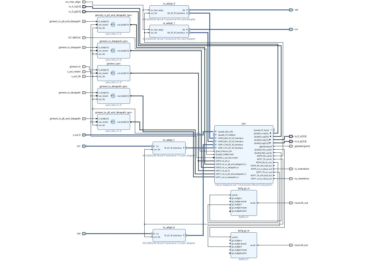
Signal Description
Name |
Description |
|---|---|
GT_REFCLK |
Reference clock input to the transceivers |
gtpowergood |
Power good output from the transceivers, the reset inputs are only valid when this signal is high |
gtreset_in |
Master reset input to the transceivers |
gtreset_[rx/tx]_datapath |
RX/TX datapath reset input to the transceivers |
gtreset_[rx/tx]_pll_and_datapath |
RX/TX PLL and datapath reset input to the transceivers |
[rx/tx]_resetdone |
RX/TX reset done output from the transceivers, indicates that the reset sequence has completed |
rxusrclk_out |
RX user clock output, the JESD204 link clock (24.75 Gbps / 66 = 375 MHz in this example) |
txusrclk_out |
TX user clock output, the JESD204 link clock (24.75 Gbps / 66 = 375 MHz in this example) |
rx_0_[n/p] |
RX differential serial data inputs |
tx_0_[n/p] |
TX differential serial data outputs |
rx_[0/1] |
RX parallel data output for the link layer |
tx_[0/1] |
TX parallel data input from the link layer |
Example usage of the Versal Transceiver Subsystem wrapper in a JESD204B/C design
One example of usage of the Versal Transceiver Subsystem wrapper can be found in the ad9081_fmca_ebz reference design: adi_axi_jesd204_rx_create.
The wrapper is called with all the necessary parameters to configure the transceivers for a specific use case.