

Source Synchronous Interface
This page presents a possible design solution for a source synchronous interface, which can be used to interface any converter that has a source synchronous data interface. The main focus is on the generic interface architecture; information regarding FPGA vendor specific hardware modules and IPs can be found on the respective FPGA manufacturer site, some of which are linked in the References section below.
What is a Source Synchronous Interface?
A source synchronous interface is a common interface type for chip-to-chip communication. The base idea behind the interface is to send a copy of the clock along with the data, which simplifies the timing model of the interface. This interface type is a successor of the system synchronous interface, where both the source and destination IC receive the clock from a common source (clock generator IC).
Architecture
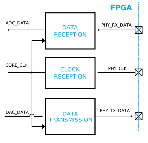
In general, a source synchronous interface consists of a clock reception module, which contains all the necessary IO resource instances to receive the digital interface clock from the device. Depending on the device type, it may also contain a data reception and/or a data transmission module. The interface exposed to the FPGA logic is a simplified FIFO interface, described in more detail here.
The CORE_CLK can have the same frequency as the PHY_CLK, or an
integer division of the PHY_CLK frequency. The general rule of thumb is
to keep the CORE_CLK frequency below 200 MHz, since it is used throughout
the data path and a too high CORE_CLK can significantly reduce the timing
margins, making it difficult (or impossible) to close timing.
If the frequency of the PHY_CLK is too high, SERDES macros are used to
convert the interface clock and data rate into a more manageable level.
Implementation with AMD Xilinx FPGAs
Files
Name |
Description |
|---|---|
Clock reception module, contains an input clock buffer and a global clock buffer for distribution. |
|
Data reception module, general architecture: |
|
Data transmission module, general architecture: |
|
Clock reception module for SERDES architecture, general architecture:
|
|
Data reception module, general architecture: |
|
Data transmission module, general architecture: |
References
Implementation with Intel/Altera FPGAs
Note
The Intel/Altera implementation of this interface is not documented yet.