Functional Safety Ready Features

Introduction

The AD-EthernetAPLDevice-SL has a failure modes, effects, and diagnostics analysis (FMEDA) document readily available upon request to support functional safety designs despite it not being assessed for functional safety. It also utilizes ADI functional safety certified components like the MAX42500 and ADFS7124-4 as diagnostics to further improve systematic capability and functional safety compliance. Furthermore, this reference design demonstrates how such FS-certified parts can be implemented in an actual system.

FMEDA Target/Requirements Overview

The aim of FMEDA is to demonstrate that the safety requirements (PFDavg and SFF), based on the assumptions of the document (or safety concept if available) and product requirement specifications, are met as shown in the summary found in Table 1, or if necessary, to make suggestions for improvement. Consider that the reference design is only a first demonstrator hardware which shall be checked to be “SIL 2 Low Demand” functional safety-ready board, the AD-EthernetAPLDevice-SL does not require to have a safety concept document initially. However, the board must still undergo on the FMEDA process with some common assumptions on its safe states, to verify that it will be at least functional safety ready.

Table 1 Targets for Safety Function of AD-EthernetAPLDevice-SL

Subject

Requirements

Targets of Safety Function

SIL2 low demand according to IEC-61508

Wording of the Safety Function

The AD-EthernetAPLDevice-SL shall measure a temperature value with a connected RTD or thermocouple sensor at the TEMP connector and transmit this value over the APL connector with a functional safe protocol.

Safe State (Assumption)

There are two possible safe states:

a) The safe bus communication over APL with the Hockey Puck is not possible anymore.

b) The Hockey Puck is indicating an internal error over the safe bus protocol and mark the transmitted temperature measurement as faulty.

Targets of safety parameter according to IEC-61508

PFD (percentage) of SIL2 ? 35% of 10^-2

PFD (avg) ? 3.5 x 10^-3

Circuit parts with type-B components:

HFT=0 ? SFF ? 90%

Timing

Proof test interval ? 12 months

Safe reaction time ? 1s

Max. internal diagnosis time ? 8h

Low demand mode

Table 2 General FMEDA Definitions

Subject

Requirements

Standard for determination of failure rates

Siemens Standard SN29500

Environmental Conditions

The analysis shall be performed for T = 40°C

Height (for soft errors): ≤ 2000m

Other requirements to be fulfilled via FMEDA

Proof of absence of feedback for the non-safety parts to the safety function

All functional safety documentation like safety manuals and FMEDA are available upon request and may require non-disclosure agreement as part of confidentiality terms.

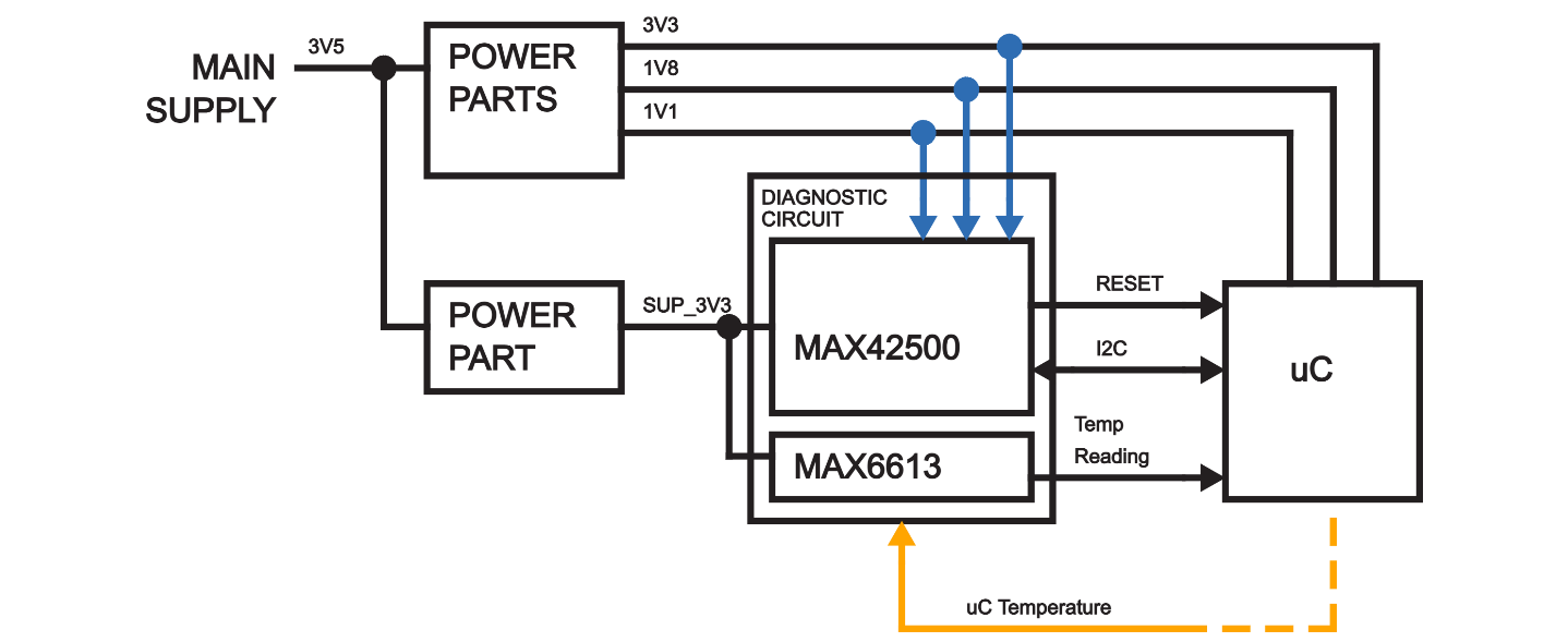
Diagnostic Circuit for Safe Microcontroller and Internal Power Supplies

In the functional safety circuit of AD-EthernetAPLDevice-SL, the main microcontroller MAX32690 is connecting its RESET pin to the MAX42500 supervisor, the supervisor mainly monitors the voltage amplitudes of the main three supplies powering the MAX32690 which are the 3.3V, 1.8V and 1.1V supplies. If at least one of those supplies deviate away from its intended amplitude, the supervisor will trigger a reset on the microcontroller. Additional feature of MAX42500 is the challenge/response watchdog timer when connected to the I2C pins of the MAX32690, the watchdog is refreshed through the I2C interface. When configured as a challenge/response watchdog, there is a key value register indicated in the MAX42500 datasheet that must be read and used to compute the appropriate response. The watchdog has several status bits to communicate status and past faults. Separate flags are provided to indicate an update-too-early fault, a wrong-key fault, and a no-update-received fault. These fields are cleared when read, this is for implementation of simple windowed watchdog.

The MAX42500 is an IEC 61508 SIL-3 certified four-to-seven-channel power supply monitor with windowed watchdog timer enabled by default as well its associated timing included. Two variants with corresponding enabled trims as shown in Table 3 are currently available. The AD-EthernetAPLDevice-SL uses the MAX42500ATEAA+T which utilizes only three channels.

Table 3 Default Voltage Monitoring Channels

PART

CH1

CH2

CH3

CH4

CH5

CH6

CH6

CH7

CH7

(V)

(V)

(V)

(V)

OV (V)

UV (V)

OV (V)

UV (V)

MAX42500ATEDA+

1.2

1.1

1.8

3.3

5

0.9

0.8

0.9

0.8

MAX42500ATEDA+T

1.2

1.1

1.8

3.3

5

0.9

0.8

0.9

0.8

MAX42500ATEAA+

1.1

1.8

3.3

MAX42500ATEAA+T

1.1

1.8

3.3

In addition, besides voltage monitoring of the microcontroller, there is also a temperature monitoring of MAX32690 using the MAX6613 small-packaged temperature sensor IC. The MAX6613 is connected and placed near the MAX32690 to sense the temperature of the microcontroller, then it sends the reading of temperature in a form of analog voltage into one of the analog input pins of MAX32690.

The combination of the MAX42500 supply monitoring and MAX6613 temperature monitoring formed the diagnostics circuit of the microcontroller MAX32690. To ensure that the diagnostic circuit will detect the microcontroller’s failure, it is important to have the power supply rail of the diagnostic components separate from the power rails monitored. This will provide a level of independence between the diagnostic circuits and the microcontroller. For example, if the MAX42500 and MAX6613 need a VDD of 3.3V, and there is a 3.3V line powering the microcontroller and being monitored by MAX42500. The diagnostic components should not tap on the supply pins on that monitored main 3.3V line, instead there should be another power part producing a separate 3.3V line that will supply the diagnostic parts. This is because the voltage being referenced by the supervisor and temperature sensor are based on its supply pin voltage, if the tapped 3.3V voltage fails or deviates then it will cause for the incorrect amplitude reading of the parts, or worse, the diagnostic parts will fail to power up at all.

Diagnostic Circuit for the Microcontroller

Figure 1 Diagnostic Circuit for the Microcontroller

ADFS7124-4 Diagnostic Features

The ADFS7124-4 is another variant of the previously released AD7124-4, 24-Bit, Sigma-Delta ADC with PGA and Reference built-in, with addition of self- diagnostics features to comply with FS. The ADFS7124-4 is compliant to SC3 by TÜV Rheinland. The diagnostic functions, which aid safe integrity level (SIL) certification, are based on the following features of the component, if ever the user wants to use these features:

1. SIGNAL CHAIN CHECK - ADFS7124-4 can check all voltages connected to the device.

2. REFERENCE DETECT - ADFS7124-4 includes on-chip circuitry to detect if there is a valid reference for conversions or calibrations when selecting an external reference as the reference source.

3. CALIBRATION, CONVERSION, AND SATURATION ERRORS - These diagnostics check the analog input used as well as the modulator and digital filter during conversions or calibration.

4. OVERVOLTAGE/UNDERVOLTAGE DETECTION - The overvoltage/undervoltage monitors check the absolute voltage on the AINx analog input pins.

5. POWER SUPPLY MONITORS - Along with converting external voltages, the ADC can monitor the voltages on the Analog Supply pin and Digital I/O Supply pins of the ADC.

6. LDO CAPACITOR DETECT - The analog and digital LDOs require an external decoupling capacitor of at least 0.1 µF. The ADFS7124-4 can check for the presence of this decoupling capacitor.

7. MCLK COUNTER - The ADFS7124-4 allows the user to monitor the controller clock. A stable controller clock is important as the output data rate, filter settling time, and the filter notch frequencies are dependent on the controller clock.

8. SPI SCLK COUNTER - The SPI SCLK counter counts the number of SCLK pulses used in each read and write operation.

9. SPI READ/WRITE ERRORS - The ADFS7124-4 can check the read and write operations to ensure that valid registers are being addressed.

10. CHECKSUM PROTECTION - Using the checksum ensures that only valid data is written to a register and allows data read from a register to be validated.

11. BURNOUT CURRENTS - The ADFS7124-4 contains two constant current generators that can be programmed to 0.5 µA, 2 µA, or 4 µA. Use these currents to verify that an external transducer is still operational before attempting to take measurements on that channel.

12. TEMPERATURE SENSOR - The ADFS7124-4 has an embedded temperature sensor that is useful to monitor the die temperature of the IC.

All the diagnostics are explained further on how to use them in the ADFS7124-4 datasheet. The safety manual is also available for this part; it can be acquired upon request.

Derating Analysis

All the components of the reference design undergo derating analysis for safety relevance, verifying that all electronic and/or electrical components are operating within limits even after derating it. Justification for operating any hardware elements at their limits shall be documented (see IEC 61508-1, Clause 5), which means all the parts in the Bill of Materials of the device are in derating analysis.

Where de-rating is appropriate, a de-rating factor of approximately two-thirds (2/3) or 67% is typical. This is also known as Safety Ratio.

For example, if the operating current flowing in a diode is 50mA, that particular diode should have high enough maximum current rating, that even if multiplied to 2/3 or 67%, it still above 50mA, like a diode with maximum current of 100mA, which 100*(2/3) = 67mA, then 67mA is greater than 50mA, so it still passed. If the maximum derated current is below 50mA then it is failed, and the user must find an alternative diode with better current rating.

The reference design components are derated to all electrical parameters be it voltage, current, power and operating temperature. It can be all parameters or can be just some parameters depending on how the components operate. A table of summary on what parameters are analyzed is included for the common part types used in the reference design.

Table 4 Parameters Needed for Derating Analysis

Component Type

Voltage Derating

Current Derating

Power Derating

Junction or Die Temperature

Temperature Range

Capacitors

Voltage maximum

Ripple Current

Temperature maximum

Operating temperatures

Connectors or Ports

Current maximum per pin

Operating temperatures

Diodes for Suppression (TVS)

Operating temperatures

Diodes for General Purpose (Silicon, Schottky)

Reverse breakdown or blocking voltage

Forward current maximum

Power maximum

Temperature maximum

Operating temperatures

Diodes for Stabilization (Zener)

Reverse or Zener current maximum

Power maximum

Temperature maximum

Operating temperatures

Analog Integrated Circuit

Wide supply maximum voltage

Load current maximum

Power maximum

Temperature maximum

Operating temperatures

Digital Integrated Circuit

Wide supply maximum voltage

Load current maximum

Power maximum

Temperature maximum

Operating temperatures

Inductors and Transformers

Average or RMS current

Operating temperatures

Quartz, Crystals or Oscillators

Operating temperatures

Resistors

Voltage maximum

Current maximum via Ohm’s Law

Power maximum

Temperature maximum

Operating temperatures

Besides which parameters to analyze, it’s important that generic parameters are established when initiating the derating analysis, especially if ambient temperature is involved.

Table 5 Generic Parameters for AD-EthernetAPLDevice-SL

Parameter

Unit

Value

Safey Ratio

%

67

Minimum Ambient Temperature

°C

-40

Maximum Ambient Temperature

°C

90

Minimum Storage Temperature

°C

-40

Maximum Storage Temperature

°C

85

Junction Temperature (ΔTmax –ΔT))

K

3