EVAL-CN0583-SOM
Multistandard Micropower Verified Smoke Detection System-on-Module.
Overview
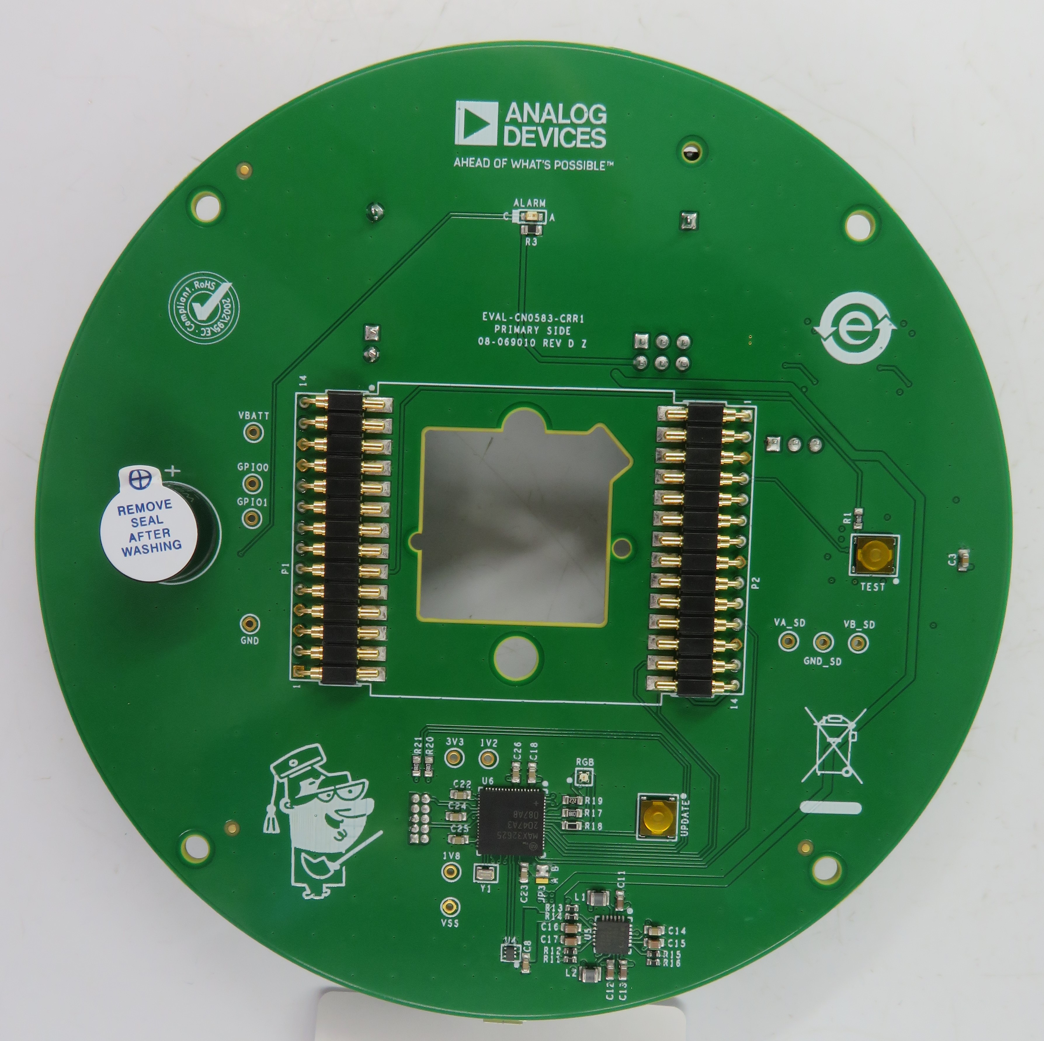
The hardware used for evaluation of the CN0583 smoke detector module is composed of two parts — the EVAL-CN0583-SOM smoke detector system-on-module (SOM), and the EVAL-CN0583-CRR1 carrier board.
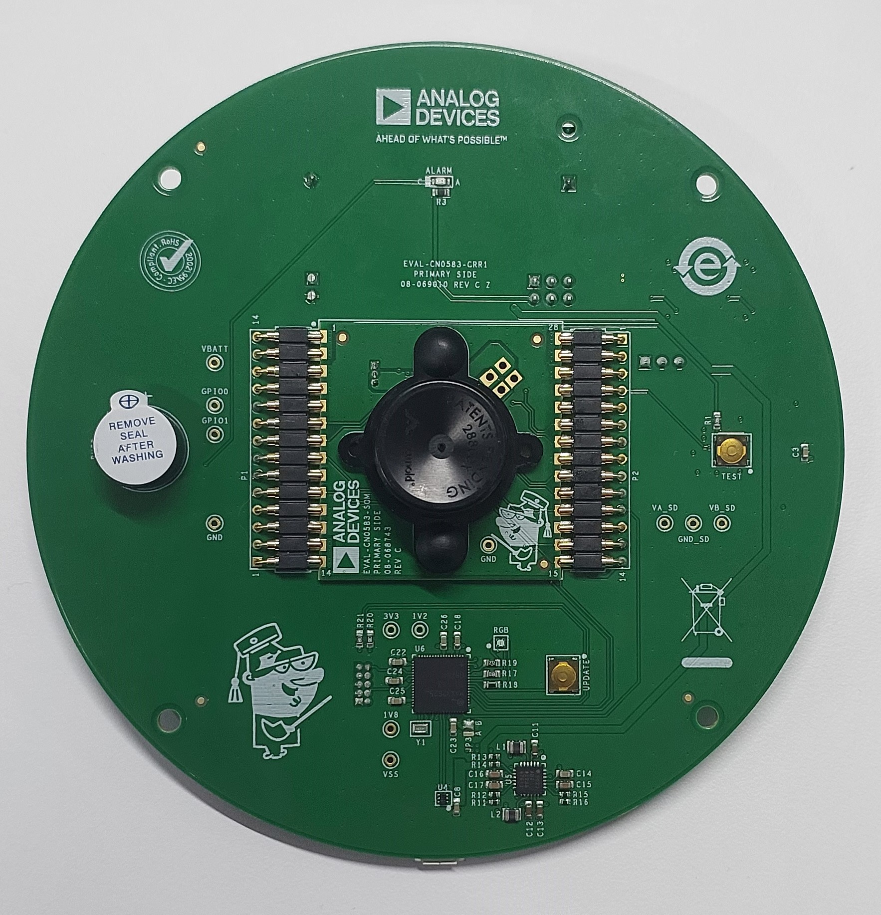
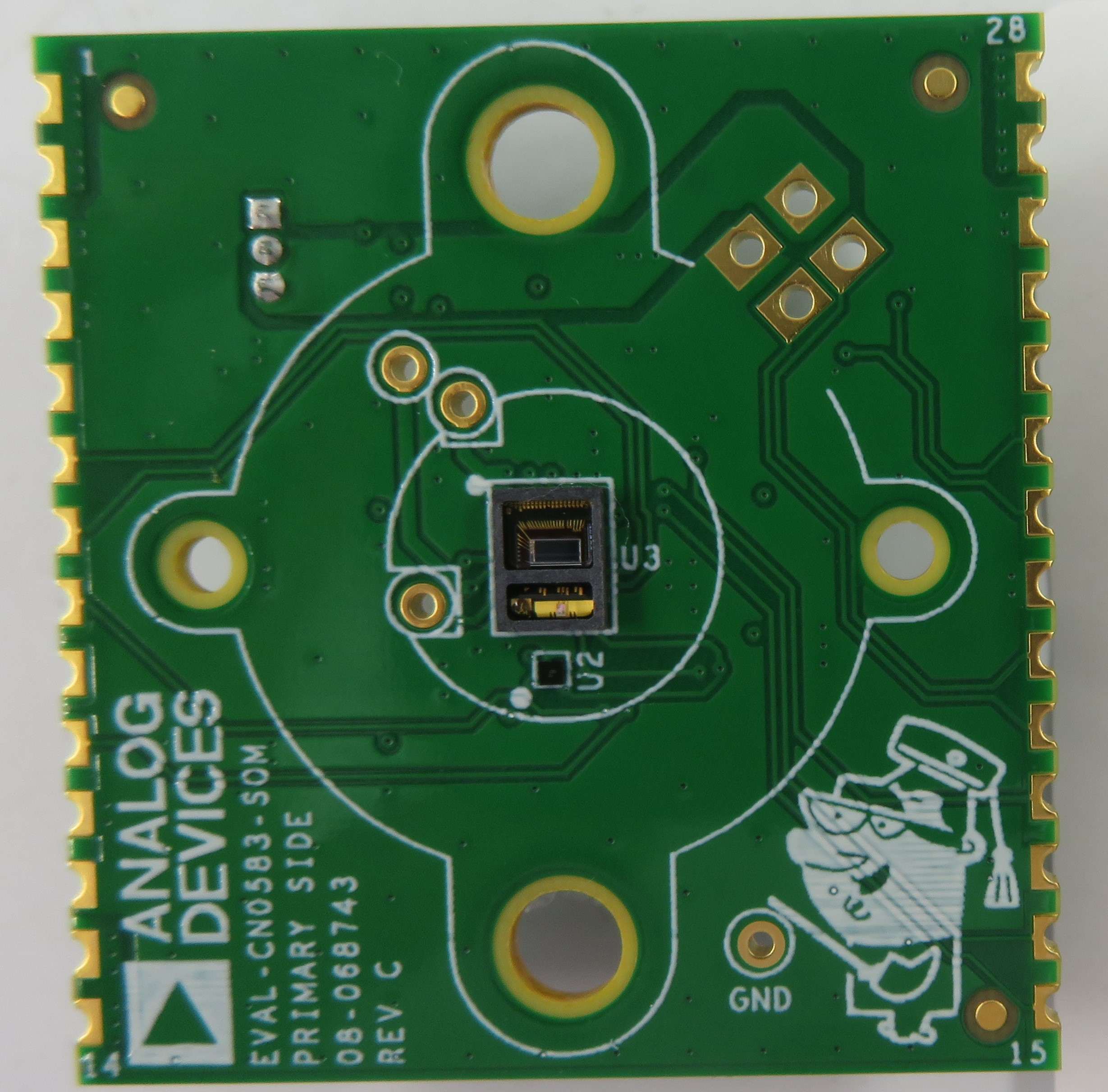
The EVAL-CN0583-SOM is a standalone module designed for development of smoke detection applications. The CN0583 SOM integrates an ADPD188BI smoke sensor, a MAX32660 microcontroller, and regulated DC power supplies needed for proper operation.
The SOM only requires DC power and ground connections from a host system to run a smoke detection application, and will output an alarm signal via a GPIO pin.
The EVAL-CN0583-CRR1 is an easy-to-use carrier board developed for evaluation of the SOM and enable rapid prototyping. The CN0583 carrier board has an onboard debugger based on the MAX32625PICO that allows drag-and-drop programming of the SOM and USB-UART communication. An indicator LED and buzzer are also included on the board to allow users to implement a basic alarm function in their smoke detector application.
System-on-Module
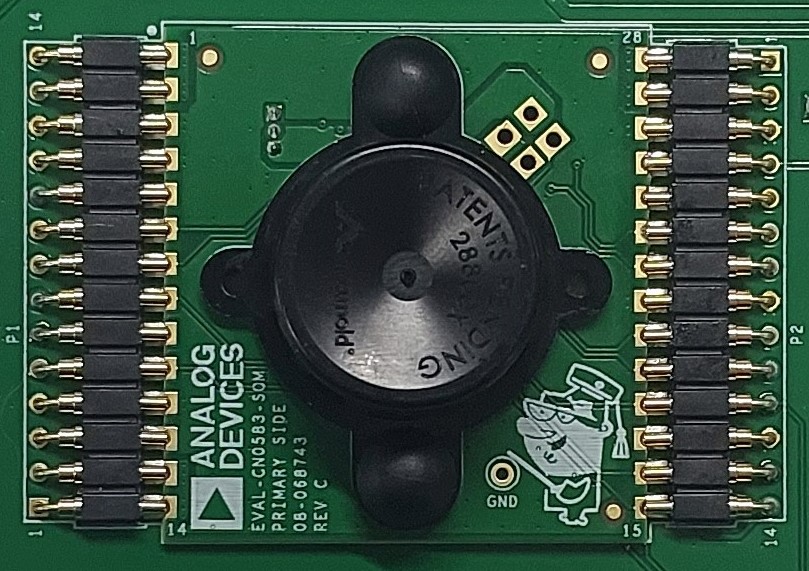
Board Castellated Pins
The SOM has 28 castellated “pins” divided into two 14-pin rows and arranged in a dual in-line pattern. These pins are used to supply power and interface external circuitry with the SOM hardware, allowing access to the GPIO pins of the MAX32660 and ADPD188BI. The table below shows the default pinout of the SOM when programmed with the CN0583 demo application.
Refer to the ADPD188BI and MAX32660 data sheets for details on the available functions of their respective GPIO pins.
Tip
The actual functions of the digital pins are user-configurable and are determined by how the MAX32660 GPIO pins are configured in the SOM firmware. When changing the pin assignments, check if the new pinout will conflict with the onboard circuity of the carrier board.
Important
Do not set P0.0 and P0.1 to any other function besides SWDIO and SWDCLK to avoid issues with reprogramming the SOM using the carrier board.
If this was accidentally done and there is a need to upload a new firmware, the flash memory of the MAX32660 must first be erased prior to reprogramming. To do this, install Maxim Microcontrollers SDK and Visual Studio Code, then perform the following steps:
Create a new project from MaximSDK’s examples for MAX32660 in Visual Studio Code.
Build this project with the ‘build’ task in Visual Studio Code.
Connect the RESET pin of the SOM to any GND pin.
Run the
erase flashtask in Visual Studio Code. (You may see a ‘target not halted’ message on the terminal, but this is expected).Disconnect the RESET pin of the SOM from GND.
Power cycle the SOM by disconnecting the power source, and then immediately reconnecting it afterward.
UART Cable Connection
There are 4 test points on the SOM that can be used to access the UART port of the MAX32660 with an external cable. This can be used to configure the smoke detector module during run time, or stream the measured data back to a serial terminal program.
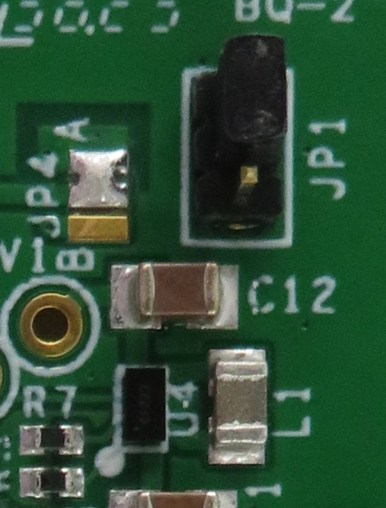
Input power to the SOM can be supplied either through the VBATT pins on the board castellated pins, or via pin 1 of JP1.
Refer to the table below on setting the JP1 and JP4 jumpers to select the power source.
Jumper Configuration |
Function |
|
|---|---|---|
JP1 |
JP4 |
|
1:2 |
A/B |
Input power is sourced from the carrier board via the VBATT pins. Default. |
2:3 |
B |
Input power is sourced from a UART cable via the P1 test points. |
LED Supply Voltage Configuration
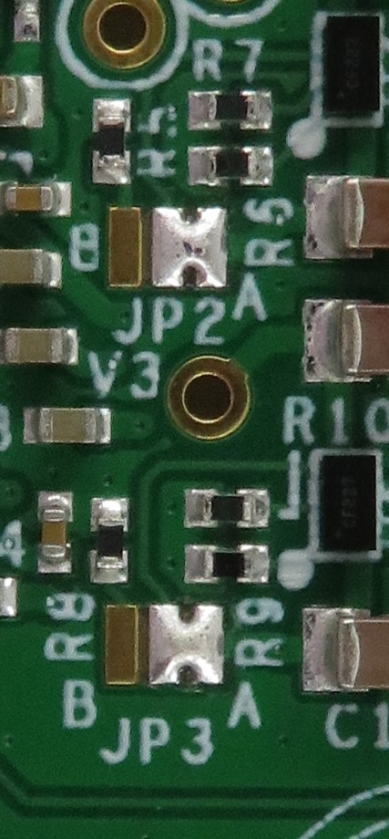
Depending on your specific power and application requirements, it may be desirable to only supply power to one of the internal LEDs of the ADPD188BI. Refer to the table below on setting the JP2 and JP3 jumpers to enable the LED supply voltages.
Carrier Board
The EVAL-CN0583-CRR1 is a carrier board designed to directly mount the EVAL-CN0583-SOM and emulate a traditional smoke detector application.
SOM Mounting
The two rows of pogo pins (P1, P2) are spring-loaded connectors used to mount the SOM. The SOM is inserted between these connectors “one side at a time” by aligning one castellated edge with a row of carrier board pogo pins, and then pressing into them. Once one row of pins has been pushed in, the other side of the SOM can be lowered and similarly inserted. Once released, the SOM will be mechanically secured with each of the castellated pin electrically connected with the pogo pins.
Power Source Options
Depending on the application requirements, input power to the SOM can be supplied in one of three ways. To select the power source, adjust the setting of JP1 as listed in the table below.
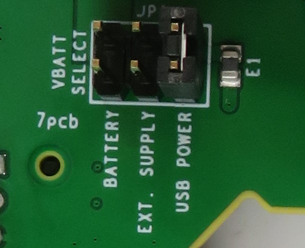
Jumper |
Configuration |
Input Power |
|---|---|---|
JP1 |
BATTERY |
CR123A battery. |
EXT SUPPLY |
External 2.2V to 5.5V power via the P3 header. |
|
USB POWER |
USB bus power via the P6 connector. Default |
Important
Only the input power source of the SOM can be switched using jumper JP1. The onboard programmer/debugger on the carrier board will always draw power from the USB connector.
LED Indicators
There are two LEDs on the CN0583 carrier board.
The ALARM LED can be used as a visual indicator in the smoke detection application loaded on the SOM (e.g., showing when an alarm condition is reached). This LED is connected to P0.4 of the MAX32660 on the SOM via pin 7 of P1.
RGB LED is used in the debugger interface of the carrier board, and will blink when there is activity (e.g., sending commands to the SOM, updating the debugger firmware).
Buzzer
The buzzer on the carrier board can be used as an audible alarm for the smoke detector application loaded on the SOM. This is connected to P0.5 of the MAX32660 on the SOM via pin 5 of P1.
Data Storage
The carrier board includes a micro-SD card slot to enable storage of smoke data. To enable/disable this function, adjust the setting of jumper JP2 as listed in the table below.
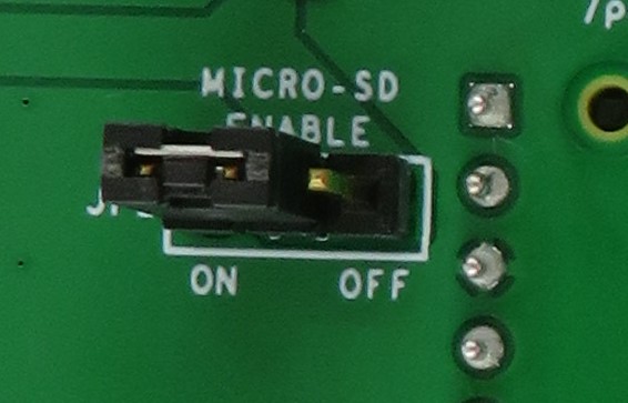
Jumper |
Configuration |
Function |
|---|---|---|
JP2 |
ON |
Enable micro-SD card functionality. Default |
OFF |
Disable micro-SD card functionality. |
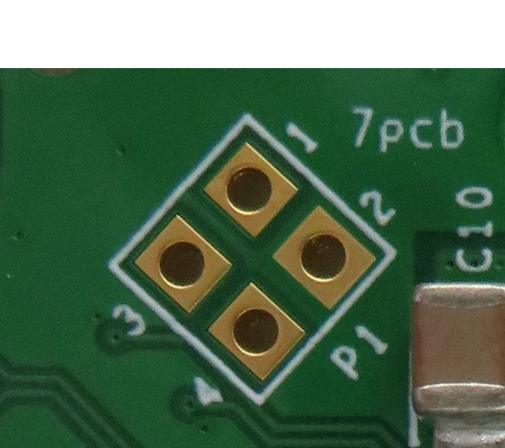
Programming the Debugger
The debugger circuit used in the carrier board is based on the MAX32625PICO application platform. By default, the included MAX32625 is already programmed with a bootloader and DAPLINK application firmware so that it can be used immediately out of the box. The included bootloader can be enabled by holding the UPDATE button while powering on the board. If necessary however, the MAX32625 can be reprogrammed via the SWD signals available on a keyed 10-pin connector (P7).
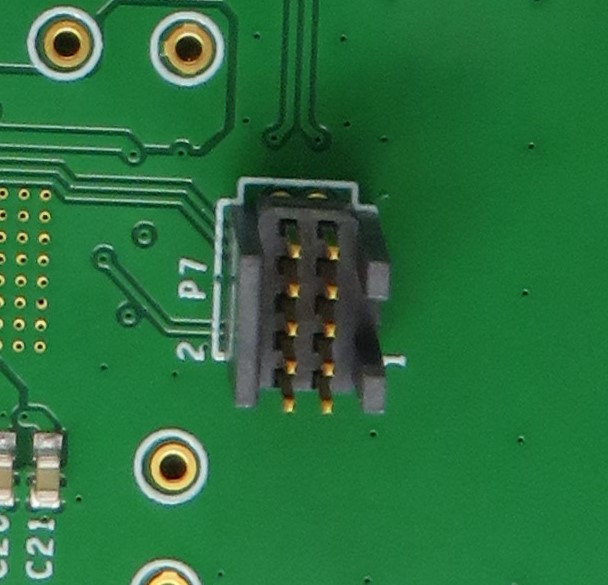
Pin Number |
Pin Name |
Function |
|---|---|---|
1 |
VTREF |
Logic-Level Reference Voltage for the SWD interface. Connected to VDDIO (1.8V) of the MAX32625. |
2 |
SWDIO |
SWD Data I/O. Connected to TMS/SWDIO of the MAX32625. |
3 |
GND |
Ground. |
4 |
SWCLK |
SWD Clock. Connected to TCK/SWDCLK of the MAX32625. |
5 |
GND |
Ground. |
6 |
DBG_TX |
UART Tx. Connected to P2.1 of the MAX32625. |
7 |
NC |
No connection. |
8 |
DBG_RX |
UART Rx. Connected to P2.0 of the MAX32625. |
9 |
NC |
No connection. |
10 |
RST |
Software Reset. Connected to SRSTN of the MAX32625. |
CN0583 Example Demo
Demo Requirements
The following are required to implement the example CN0583 demo application:
ADPD188BI Smoke Chamber (Included with the SOM)
Micro-SD Card (Optional)
USB Micro-B Cable
Computer (Must have a serial terminal installed)
Hardware Setup
Install the ADPD188BI smoke chamber on the primary side of the SOM.
Carefully insert the SOM between P1 and P2 of the carrier board, following the cutout on the center. The proper orientation of the module will have Pin 1 closest to the buzzer, and Pin 28 on the side with the test button.
Connect the P6 on the carrier board to the computer using the micro-USB cable.
On the computer, check if the CN0583 hardware setup is recognized as a DAPLINK drive. This will indicate that the necessary drivers are complete and correct.
Programming the SOM
This step is only required if you want to update the firmware of the CN0583 SOM. The programming may be done over DAPLINK, as following:
Download the hex file for the demo application. Alternatively, you may use your own hex file.
Download
Algorithm for UL 217 8th Edition Standard: UL 217 hex with CLI stream
Algorithm for EN14604:2005 Standard: EN14604 hex with CLI stream
No Algorithm: no-alarm CLI hex
Connect the EVAL-CN0583-CRR1 carrier board to your PC using an USB cable.
Wait for the DAPLINK directory to appear on your PC’s filesystem.
Copy the hex file to the DAPLINK directory.
The hex file will now be written in the MAX32660’s flash memory (this should take a few seconds). After that, the DAPLINK directory will be deleted.
Wait for the DAPLINK directory to be created again (without unplugging the USB cable). After that, the CN0583 SOM is programmed with the new firmware. You may now use the CLI application by following the steps in the next section.
Serial Terminal Setup
A serial terminal is an application that runs on a PC or laptop that is used to display data and interact with a connected device (including many of the Circuits from the Lab reference designs). The device’s UART peripheral is most often connected to a UART to USB interface IC, which appears as a traditional COM port on the host PC/ laptop. (Traditionally, the device’s UART port would have been connected to an RS-232 line driver / receiver and connected to the PC via a 9-pin or 25-pin serial port.) There are many open-source applications, and while there are many choices, typically we use one of the following:
Before continuing, please make sure you download and install one of the above programs.
There are several parameters on all serial terminal programs that must be setup properly in order for the PC and the connected device to communicate. Below are the common settings that must match on both the PC side and the connected UART device.
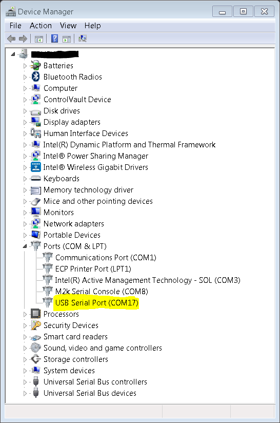
COM Port - This is the physical connection made to your PC or laptop, typically made through a USB cable but can be any serial communications cable. You can determine the COM port assigned to your device by visiting the device manager on your computer. Another method for identifying which COM port is associated with a USB-based device is to look at which COM ports are present before plugging in your device, then plug in your device, and look for a new COM port.
Baud Rate - This is the speed at which data is being transferred from the connected device to your PC. These parameters must be the same on both devices or data will be corrupted. The default setting for most of the reference designs in 115200.
Data Bits - The number of data bits per transfer. Typically, UART transmits ASCII codes back to the serial port so by default this is almost always set to 8-Bits.
Stop Bits - The number of “stop” conditions per transmission. For the CN0583 demo, this should be set to 2 for redundancy.
Parity - Is a way to check for errors during the UART transmission. Unless otherwise specified, set parity to “none”.
Flow Control - Is a way to ensure that data lose between fast and slow devices on the same UART bus are not lost during transmission. This is typically not implemented in a simple system, and unless otherwise specified, set to “none”.
In many instances there are other options that each of the different serial terminal applications provide, such as local line echo or local line editing, and features like this can be turned on or off depending on your preferences. This setup guide will not go over all the options of each tool, but just the minor features that will make it easier to read back data from the connected devices.
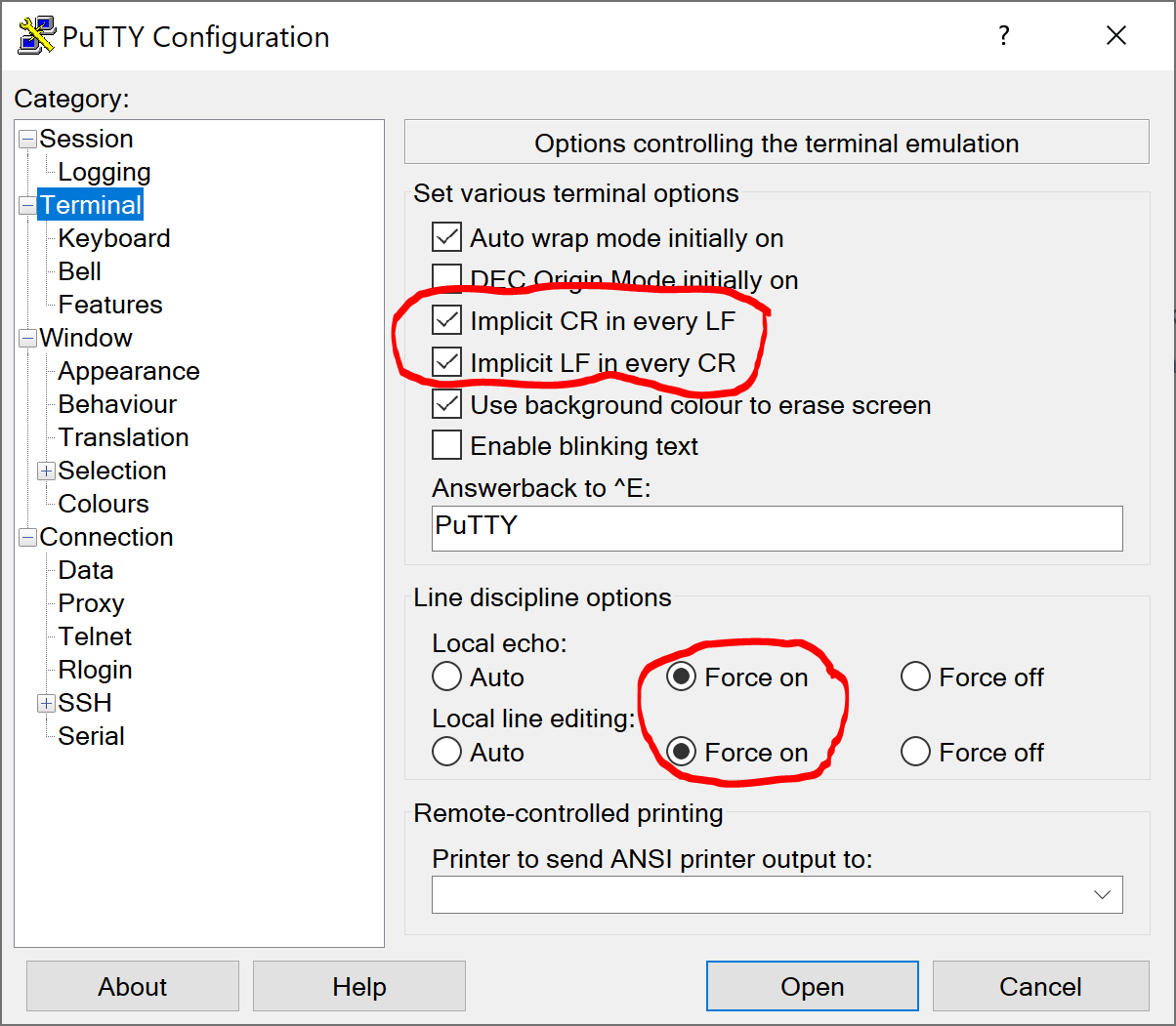
Example setup using PuTTY
Plug in your connected device using a USB cable or other serial cable.
Wait for the device driver of the connected device to install on your PC or Laptop.
Open your device manager, and find out which COM port was assigned to your device.
Open up your serial terminal program (e.g., PuTTY).
Click on the serial configuration tab or window, and input the settings to match the requirements of your connected device. The default baud rate for most of the reference designs is 115200. Make sure that you use the correct baud rate for your application.
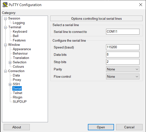
Ensure you click on the checkboxes for Implicit CR in every LF and Implicit LF in every CF.
Ensure that local echo and line editing are enabled, so that you can see what you type and are able to correct mistakes. (Some devices may echo typed characters - if so, you will see each typed character twice. If this happens, turn off local echo.)
Click on the
Openbutton, and as long as your connected device and serial terminal program are setup the same, then you should be able to start entering commands.
Available Commands
Typing help (or simply h) after the initial calibration sequence will display the list of commands and their shortened versions.
Tip
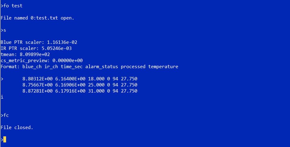
By default, the output mode and data rate are set to PTR and 0.163 (1/6) samples per second, respectively.
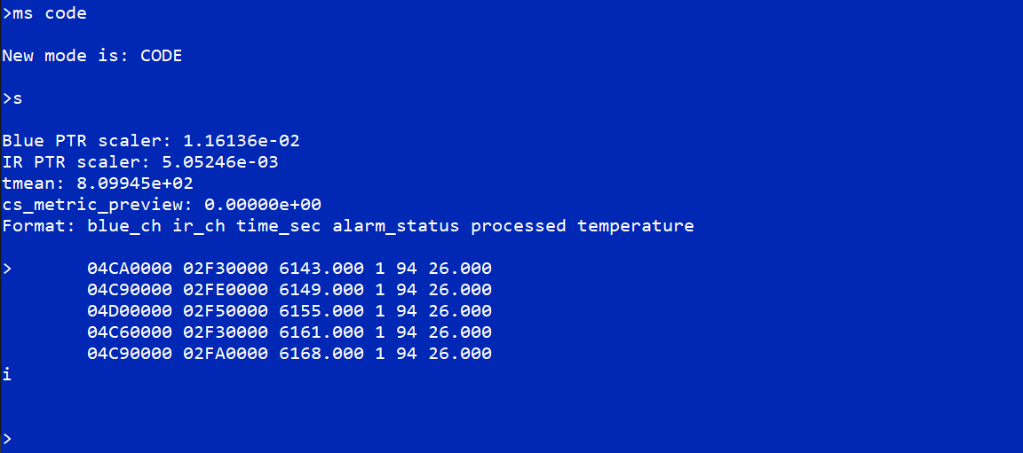
Example Output Data
Below are examples of the CN0583 boards outputting data in PTR and raw codes and then exiting after several samples:
Test Results
Using the CN0583 hardware and the ADSW-SMOKEALGO-PRODLIC algorithm, the setup was tested at a certified testing facility (Intertek) and passed all the smoke sensor aspects of the UL-217 8th Edition Standards. You can view the entire report below:
The hardware and algorithm were also verified using the EN54-7/EN14604 Standard and the results are available here:
Device Driver Support
There are no-OS drivers provided for controlling the digital devices on the CN0583 boards.
Schematic, PCB Layout, Bill of Materials
Download
Schematics
PCB Layout
Bill of Materials
Allegro Project
Assembly Drawing
Additional Information and Useful Links
Help and Support
For questions and more information, please visit the EngineerZone.