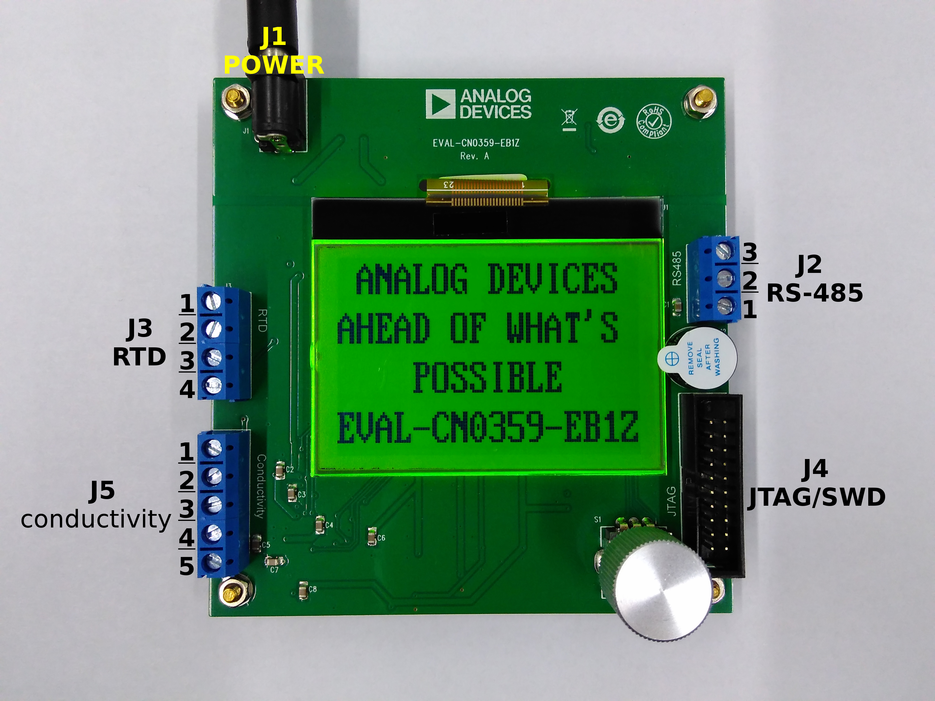
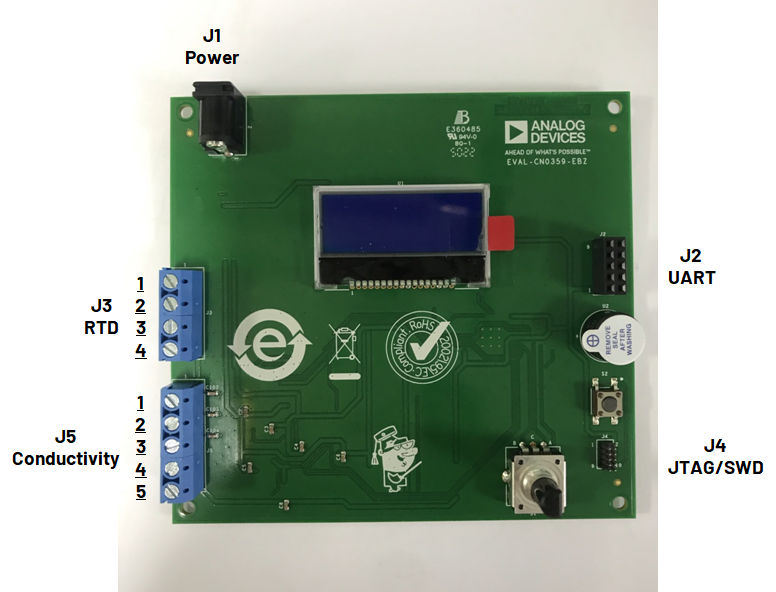
EVAL-CN0359-EBZ
Fully Automatic High Performance Conductivity Measurement System.
Overview
The CN0359 is a complete, highly accurate conductivity measurement system designed for applications involving ionic content measurement of liquids, water quality analysis, industrial quality control, and chemical analysis.
A carefully selected combination of precision signal conditioning components yields an accuracy of better than 0.3% over a conductivity range of 0.1 μS to 10 S (10 MΩ to 0.1 Ω) with no calibration requirements. Automatic detection is provided for either 100 Ω or 1000 Ω platinum (Pt) resistance temperature devices (RTDs), allowing the conductivity measurement to be referenced to 25°C.
The system accommodates 2-wire and 4-wire conductivity cells, and 2-wire, 3-wire, and 4-wire RTDs for improved accuracy and flexibility.
Hardware Connections
The following sections will describe the hardware in more detail.
The CN0359 have 5 connectors:
J1 for power supply
J2 for RS-485 communication (Rev A) or UART communication (Rev B)
J3 for RTD temperature sensor
J4 for JTAG/SWD debug
J5 for conductivity sensor
EVAL-CN0359-EB1Z Rev. A
EVAL-CN0359-EBZ Rev. B
The following equipment are required to evaluate the CN0359:
CN0359 circuit evaluation board
EVAL-CFTL-6V-PWRZ 6V DC wall connector (or equivalent)
2-wire and 4-wire conductivity cells
2-wire and 3-wire and 4-wire PT100 and PT1000 RTDs
PC with Microsoft Windows 7 (or later OS) and USB 2.0 (or faster USB) port
USB to RS-485 converter cable (Rev A) or ADALM-UARTJTAG or similar USB to UART bridge module (Rev B)
Note
The following conductivity cells have been used to test the functionality of the CN0359:
TOPAC CS SK10T (2-electrode cell)
TOPAC CS SK40T (4-electrode cell)
The following extra equipment are require to reprogram or debug the CN0359:
J-link debug cable (or equivalent JTAG/SWD debug cable)
20-pin/10-pin JTAG/SWD adapter (Rev B only)
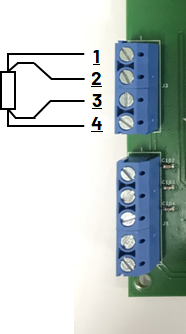
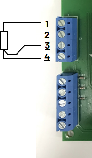
Conductivity Sensor Connections
The CN0359 supports both 2-electrode and 4-electrode types of conductivity sensors. The conductivity sensor should be connected to J5 of the evaluation board.
Refer to the following table for the pin map of J5:
Pin Number |
Signal Name |
Pin Description |
|---|---|---|
Pin 1 |
I(+) |
(+) Conductivity Probe Excitation Current Pin |
Pin 2 |
V(+) |
(+) Conductivity Probe Voltage Sense Pin |
Pin 3 |
V(-) |
(-) Conductivity Probe Voltage Sense Pin |
Pin 4 |
I(-) |
(-) Conductivity Probe Excitation Current Pin |
Pin 5 |
GND |
Ground |
Important
The error specification for the CN0359 is +/- 0.3% within the 0.1 μS to 10 S (10 MΩ to 0.1 Ω) conductivity range. If the conductivity of the solution being measured is outside this range, extra error may be introduced.
During conductivity measurement, the excitation current flows into the sensor through the I pins and then translated into a voltage signal by an onboard transimpedance amplifier. This signal, plus the voltage developed across the V pins, are then amplified and then sampled by the microcontroller ADCs.
Refer to following pictures for the proper conductivity sensor connections. Sensor connections are the same for both Rev A and Rev B evaluation boards.
2-Electrode Conductivity Sensor Connection
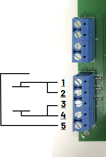
Caution
When using 2-electrode sensors with the CN0359 evaluation board:
Pin 1 ⇔ Pin 2 of J5 MUST be shorted.
Pin 3 ⇔ Pin 4 of J5 MUST be shorted.
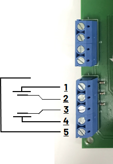
4-Electrode Conductivity Sensor Connection
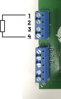
RTD Connections
The CN0359 supports PT100 and PT1000 RTD sensors connected in either 2-wire, 3-wire, or 4-wire mode; the RTD type and connection mode will be automatically detected by the software. The RTD temperature sensor should be connected to header J3 on the evaluation board.
The J3 pin map is following:
Pin Number |
Signal Name |
Pin Description |
|---|---|---|
Pin 1 |
I(+) |
(+) RTD Excitation Current Pin |
Pin 2 |
V(+) |
(+) RTD Voltage Sense Pin |
Pin 3 |
V(-) |
(-) RTD Voltage Sense Pin |
Pin 4 |
I(-) |
(-) RTD Excitation Current Pin |
During RTD measurement, constant excitation current flows into the RTD through the I pins, and the resulting voltage difference across the V pins is sampled by the microcontroller ADCs.
Refer to the following pictures for the different RTD wire mode connections. RTD connections are the same for both Rev A and Rev B evaluation boards.
RTD 4-Wire Connections
RTD 3-Wire Connections
RTD 2-Wire Connections
Data Communications Interface Connections
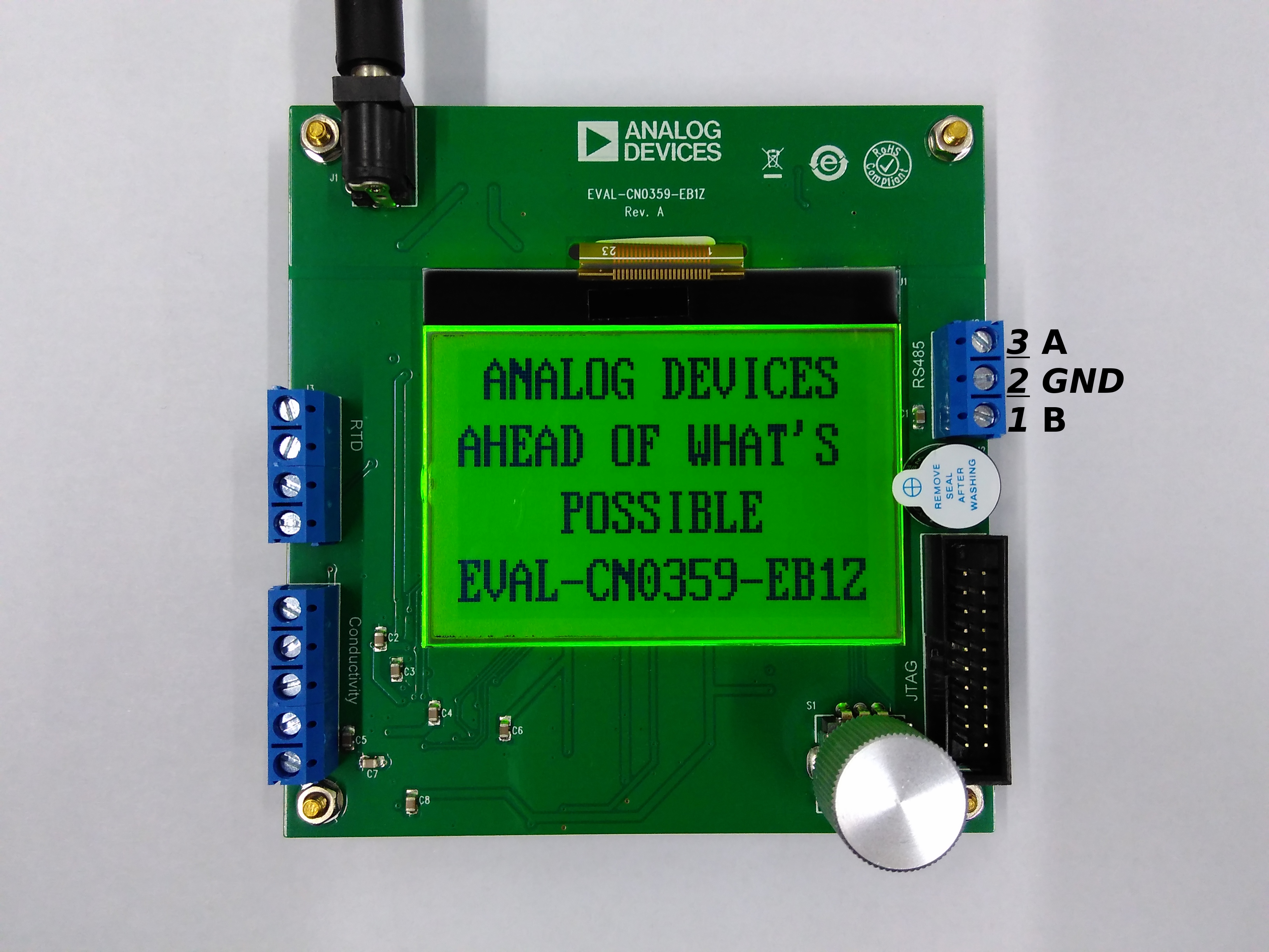
Connector J2 allows users to control the CN0359 remotely via a network. The interface supported by J2 differs based on the evaluation board revision.
Rev A: RS-485
In the Rev A evaluation boards, J2 is a terminal block with the following pin map:
Pin Number |
Signal Name |
Pin Description |
|---|---|---|
Pin 1 |
B |
RS-485 B Signal |
Pin 2 |
GND |
Ground |
Pin 3 |
A |
RS-485 A Signal |
Important
The CN0359 software is capable of supporting up to 254 boards (with RS-485 addresses from 1 to 254) connected to one RS-485 network. To improve noise performance, the RS-485 terminal resistor (R10) on the Rev A boards is set to 10 kΩ.
If multiple devices will be used on the same RS-485 network, R10 may need to be changed (or removed completely) to comply with the RS-485 standard. For more information about RS-485, refer to: an-960 or ANSI/TIA/EIA-485 standard.
J2 Pin Map (Rev A)
Rev B: UART Interface
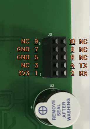
In the Rev B evaluation boards, J2 is a 2×5, 2.54 mm female header with the following pin map:
Pin Number |
Signal Name |
Pin Description |
|---|---|---|
Pin 1 |
3V3 |
3.3 V Power |
Pin 2 |
RX |
CN0359 Receive Data |
Pin 3 |
NC |
No Connection |
Pin 4 |
TX |
CN0359 Transmit Data |
Pin 5 |
GND |
Ground |
Pin 6 |
NC |
No Connection |
Pin 7 |
GND |
Ground |
Pin 8 |
NC |
No Connection |
Pin 9 |
NC |
No Connection |
Pin 10 |
NC |
No Connection |
JTAG/SWD Connections
Connector J4 allows users to debug and/or program the CN0359 through a JTAG/SWD debug probe. The physical form factor of this connector differs based on the evaluation board revision.
The JTAG/SWD debug interface on the CN0359 only supports SWD mode.
Rev A: Standard ARM JTAG
In the Rev A boards, J4 is pin compatible with SEGGER J-Link debug probes that have the standard 20-pin connector/cable. The following table shows the pin map of J4 in this case:
Pin Number |
Signal Name |
Pin Description |
|---|---|---|
Pin 1 |
VTref |
Target Reference Voltage. Connected to the 3.3 V supply rail on the CN0359. |
Pin 2 |
NC |
No Connection |
Pin 3 |
NC |
No Connection |
Pin 4 |
GND |
Ground |
Pin 5 |
NC |
No Connection |
Pin 6 |
GND |
Ground |
Pin 7 |
SWDIO |
SWD Data. Single bi-directional data line. |
Pin 8 |
GND |
Ground |
Pin 9 |
SWDCLK |
SWD Clock. Connected to the SWDCLK pin of the ADuCM360 on the CN0359. |
Pin 10 |
GND |
Ground |
Pin 11 |
NC |
No Connection |
Pin 12 |
GND |
Ground |
Pin 13 |
NC |
No Connection |
Pin 14 |
GND |
Ground |
Pin 15 |
RESET |
Target Reset Signal. Connected to the RESET pin of the ADuCM360 on the CN0359. |
Pin 16 |
GND |
Ground |
Pin 17 |
NC |
No Connection |
Pin 18 |
GND |
Ground |
Pin 19 |
NC |
No Connection |
Pin 20 |
GND |
Ground |
Rev B: Mini-JTAG
In the Rev B boards, J4 is pin compatible with SEGGER J-Link debug probes that have the smaller 10-pin connector/cable. The following table shows the pin map of J4 in this case:
Pin Number |
Signal Name |
Pin Description |
|---|---|---|
Pin 1 |
VTref |
Target Reference Voltage. Connected to the 3.3 V supply rail on the CN0359. |
Pin 2 |
SWDIO |
SWD Data. Single bi-directional data line. |
Pin 3 |
GND |
Ground |
Pin 4 |
SWDCLK |
SWD Clock. Connected to the SWDCLK pin of the ADuCM360 on the CN0359. |
Pin 5 |
GND |
Ground |
Pin 6 |
NC |
No Connection |
Pin 7 |
NC |
No Connection |
Pin 8 |
NC |
No Connection |
Pin 9 |
NC |
No Connection |
Pin 10 |
RESET |
Target Reset Signal. Connected to the RESET pin of the ADuCM360 on the CN0359. |
Usage Instructions
The CN0359 is powered from a 6V DC wall connector (EVAL-CFTL-6V-PWRZ) and will run automatically when the supply is plugged in. The conductivity and RTD measurements can be displayed using two interfaces: the onboard LCD screen or the remote network interface (RS-485 for Rev A; UART for Rev B). Both interfaces can also be used simultaneously if desired.
The CN0359 has the following settings that can be programmed by the user:
Excitation Voltage
Excitation Frequency
Track-Hold Setup Time
Track-Hold Hold Time
Temperature Coefficient
Conductivity Cell Constant
Baud Rate
RS-485 Address (Rev A only)
LCD Contrast
Warning
Always check the excitation voltage and frequency before connecting the conductivity sensor to the CN0359 evaluation board. Using a setting that is outside the specifications of the sensor can cause damage.
LCD Screen and Encoder User Interface
By default, the LCD screen will display the measurement results of the CN0359. When used with the encoder S1 however, it can instead be used to navigate a menu-based interface to configure the different CN0359 settings listed above.
General Usage Instructions
The text in the menu interface can have one of the three following states:
Normal (dark font with light background) |
Indicates an available option or value |
Reverse (light font with dark background) |
Indicates the currently selected option or value |
Blinking (switches between normal and reverse states) |
Indicates a value that is currently being edited by the user |
To interact with the menu items, the encoder S1 can be turned clockwise or counterclockwise. It has no mechanical stop, and can also be used as a push button. The following details the operation of the encoder:
Control Menu via S1 |
Equivalent Operation |
|---|---|
Turn clockwise when there is no blinking text |
Move to the next option or value |
Turn clockwise while there is blinking text |
Increase value |
Turn counterclockwise when there is no blinking text |
Go back to previous option or value |
Turn counterclockwise while there is blinking text |
Decrease value |
Push button when there is no blinking text |
Use option or start editing value |
Push button while there is blinking text |
Stop editing value |
There are two exceptions to the behavior described above:
Home or Measurement Screen |
There is no selectable option or value in this screen so turning the encoder will have no effect. Push the button to enter the main menu interface. |
LCD Contrast Setting Screen |
Turning the encoder clockwise/counterclockwise will increase/decrease LCD contrast, respectively. Push the button to return to the main menu. |
The CN0359 also has a buzzer on the evaluation board. When editing a value, it will provide an audible indication when the maximum or minimum setting has been reached.
CN0359 Start Up and LCD Contrast
The contrast of the LCD screen can be set by the user; however, if the LCD contrast is set improperly, the text may become difficult to read. If needed, the following procedure can be used to “blindly” adjust the LCD contrast:
Power up the CN0359 evaluation board. If the onboard buzzer beeps for 50 ms immediately, the system was able to load the previous settings properly.
Push the encoder button S1 within 3 seconds after powering on.
The onboard buzzer will beep for 100 ms twice, with an short interval of 100 ms in between. This indicates that the interface is now in the LCD contrast setting screen.
Turn the encoder S1 clockwise/counterclockwise to increase/decrease LCD contrast. Adjust it such that the text will appear clearly and sharply.
Push the button S1 to exit the LCD contrast setting screen.
Select the “Return to home” option in the main menu and press the button. The new LCD contrast setting should now be saved.
Buzzer and Alarm
The CN0359 evaluation board has a buzzer U2 on it that produces notification sounds during operation. The buzzer is activated in the following events:
Beeps once after connecting power to the board, and beeps again after the home/measurement screen appears.
Beeps twice if button is pushed while the splash screen is displayed during power-up. If this occurs, the interface will enter the LCD contrast setting screen.
Beeps five times rapidly if an internal error is encountered during start up. When this occurs, all settings will be reset to their default values.
Beeps whenever an RTD error is encountered while at the home/measurement screen. Check the RTD connection when this occurs.
Beeps whenever a conductivity sensor error is encountered while at the home/measurement screen. Check the sensor connection when this occurs.
Beeps when user tries to set a programmable value (e.g., EXC voltage, EXC freq, etc.) outside the acceptable range.
Data Communications Interface
Caution
To communicate with the CN0359 from a PC, use a RS-485 to USB converter (or UART to USB bridge, depending on the version of the board) and a terminal emulator such as Putty or Tera Term. Please check the settings of your software before connecting to the board. The output of the terminal program must match the following command formats.
Important
The RS-485 interface for Rev A, and the UART interface for Rev B both use char ‘\n’ LF (Line Feed) as the ending character. This means that the CN0359 will respond to a valid command immediately after receiving char ‘\n’. Please make sure that char ‘\n’ is the last byte that will be sent to CN0359 in each command string. Some serial port terminal software can automatically add char ‘\n’ to the output stream upon pressing the Return key. For software that cannot append char ‘\n’ automatically, the command string should be sent to the CN0359 in hexadecimal format with 0x0a appended.
The CN0359 software uses char ’ ’ (i.e., the space character) as a delimiter in the command string.
Rev A: RS-485 Command Usage
In this user guide, the CN0359 is referred to as the client, and the PC (or any device used to initiate communication) is referred to as the host.
The half-duplex RS-485 interface used in Rev A boards can connect multiple (up to 254) clients in the same network. All clients are kept in receive status while idle, and can only transmit data when given the appropriate command.
Warning
Only one device can send data at the a given time in this configuration; otherwise the RS-485 network will encounter signaling conflicts. If multiple hosts exist in your network, please ensure that no such conflicts occur.
Caution
The RS-485 address can only be changed through the LCD and encoder user interface. Set the desired address first prior to sending commands to the board.
The following format is used to explain the different RS-485 commands in this user guide:
SYNOPSIS
address command option
DESCRIPTION
Important
The address is the integer value of the RS-485 address, ranging from 1 to 254. The address should always go before the command and the option for proper communication to the corresponding CN0359.
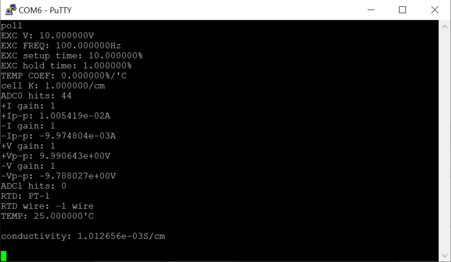
poll - Query CN0359
address poll
The poll command is used to query the CN0359 for its programmed settings and its sensor readings. For example, entering the following will query the CN0359 at address 100 for its settings and its measurements:
100 poll
setvolt - Set Excitation Voltage
address setvolt voltage
The setvolt command is used to set the peak voltage of the cell excitation signal, ranging from 0.1 V to 10 V. For example, the following command will set a 2.5 V peak excitation voltage for the CN0359 at address 100:
100 setvolt 2.5
setfreq - Set Excitation Frequency
address setfreq frequency
The setfreq command is used to set the frequency of the cell excitation signal, ranging from 10 Hz to 100000 Hz. For example, the following command will set an 85.6 Hz excitation frequency for the CN0359 at address 100:
100 setfreq 85.6
setk - Set Cell Constant
address setk K
The setk command is used to input the cell constant of the conductivity sensor used, ranging from 0.01 cm-1 to 100 cm-1. For example, the following command will input a cell constant of 1.268 cm-1 to the CN0359 at address 100:
100 setk 1.268
setcof - Set Temperature Coefficient
address setcof coefficient
The setcof command is used to input the temperature coefficient of the test sample, ranging from -10%/°C to 10%/°C. For example, the following command will input a -2.58%/°C temperature coefficient to the CN0359 at address 100:
100 setcof -2.58
setstm - Set Track-And-Hold Setup Time
address setstm time
The setstm command is used to set the track-and-hold setup time as a percentage of a half excitation period, ranging from 0% to 80%.
Note
Setup time is measured from the start of a half excitation period to the moment the CN0359 begins tracking the measurement voltages.
For example, the following command will set a 5.8% setup time for the CN0359 at address 100:
100 setcof 5.8
If the excitation frequency is 100Hz, then half of the period will be 5 ms. The track-and-hold setup time in this example will therefore be 290 μs.
sethtm - Set Track-And-Hold Hold Time
address sethtm time
The sethtm command is used to set the track-and-hold hold time as a percentage of a half excitation period, ranging from 0% to 10%.
Note
Hold time is measured from the moment the CN0359 stops tracking the measurement voltages to the end of a half excitation period.
For example, the following command will set a 1.5% hold time for the CN0359 at address 100:
100 sethtm 1.5
If the excitation frequency is 1 kHz, then half of the period will be 500 μs. The track-and-hold hold time in this example will therefore be 7.5 μs.
Rev B: UART Command Usage
The following format is used to explain the different UART commands in this user guide:
SYNOPSIS
command option
DESCRIPTION
poll - Query CN0359
poll
The poll command is used to query the CN0359 for its programmed settings and its sensor readings. For example, entering the following will query the CN0359 via UART for its settings and its measurements:
poll
Below is a sample UART output obtained using the poll command:
setvolt - Set Excitation Voltage
setvolt voltage
The setvolt command is used to set the peak voltage of the cell excitation signal, ranging from 0.1 V to 10 V. For example, the following command will set a 2.5 V peak excitation voltage for the CN0359 via UART:
setvolt 2.5
setfreq - Set Excitation Frequency
setfreq frequency
The setfreq command is used to set the frequency of the cell excitation signal, ranging from 10 Hz to 100000 Hz. For example, the following command will set an 85.6 Hz excitation frequency for the CN0359 via UART:
setfreq 85.6
setk - Set Cell Constant
setk K
The setk command is used to input the cell constant of the conductivity sensor used, ranging from 0.01 cm-1 to 100 cm-1. For example, the following command will input a cell constant of 1.268 cm-1 to the CN0359 via UART:
setk 1.268
setcof - Set Temperature Coefficient
setcof coefficient
The setcof command is used to input the temperature coefficient of the test sample, ranging from -10%/°C to 10%/°C. For example, the following command will input a -2.58%/°C temperature coefficient to the CN0359 via UART:
setcof -2.58
setstm - Set Track-And-Hold Setup Time
setstm time
The setstm command is used to set the track-and-hold setup time as a percentage of a half excitation period, ranging from 0% to 80%.
Note
Setup time is measured from the start of a half excitation period to the moment the CN0359 begins tracking the measurement voltages.
For example, the following command will set a 5.8% setup time for the CN0359 via UART:
setcof 5.8
If the excitation frequency is 100Hz, then half of the period will be 5 ms. The track-and-hold setup time in this example will therefore be 290 μs.
sethtm - Set Track-And-Hold Hold Time
sethtm time
The sethtm command is used to set the track-and-hold hold time as a percentage of a half excitation period, ranging from 0% to 10%.
Note
Hold time is measured from the moment the CN0359 stops tracking the measurement voltages to the end of a half excitation period.
For example, the following command will set a 1.5% hold time for the CN0359 via UART:
sethtm 1.5
If the excitation frequency is 1 kHz, then half of the period will be 500 μs. The track-and-hold hold time in this example will therefore be 7.5 μs.
Software Programming
This section will describe the CN0359 software and the process for programming the evaluation board.
Hardware Interface
Connector J4 allows users to debug and/or program the CN0359 through a JTAG/SWD debug probe. The physical form factor of this connector differs based on the evaluation board revision. The JTAG/SWD debug interface on the CN0359 only supports SWD mode.
Caution
A J-Link debug probe (or equivalent) is needed to download the firmware to the onboard ADuCM360 of the CN0359.
Important
Details regarding the J-Link debug probe can be found at J-Link Manual
Rev A: Standard ARM JTAG
In the Rev A boards, J4 is pin compatible with SEGGER J-Link debug probes that have the standard 20-pin connector/cable. The following table shows the pin map of J4 in this case:
Pin Number |
Signal Name |
Pin Description |
|---|---|---|
Pin 1 |
VTref |
Target Reference Voltage. Connected to the 3.3 V supply rail on the CN0359. |
Pin 2 |
NC |
No Connection |
Pin 3 |
NC |
No Connection |
Pin 4 |
GND |
Ground |
Pin 5 |
NC |
No Connection |
Pin 6 |
GND |
Ground |
Pin 7 |
SWDIO |
SWD Data. Single bi-directional data line. |
Pin 8 |
GND |
Ground |
Pin 9 |
SWDCLK |
SWD Clock. Connected to the SWDCLK pin of the ADuCM360 on the CN0359. |
Pin 10 |
GND |
Ground |
Pin 11 |
NC |
No Connection |
Pin 12 |
GND |
Ground |
Pin 13 |
NC |
No Connection |
Pin 14 |
GND |
Ground |
Pin 15 |
RESET |
Target Reset Signal. Connected to the RESET pin of the ADuCM360 on the CN0359. |
Pin 16 |
GND |
Ground |
Pin 17 |
NC |
No Connection |
Pin 18 |
GND |
Ground |
Pin 19 |
NC |
No Connection |
Pin 20 |
GND |
Ground |
Rev B: Mini-JTAG
In the Rev B boards, J4 is pin compatible with SEGGER J-Link debug probes that have the smaller 10-pin connector/cable. The following table shows the pin map of J4 in this case:
Pin Number |
Signal Name |
Pin Description |
|---|---|---|
Pin 1 |
VTref |
Target Reference Voltage. Connected to the 3.3 V supply rail on the CN0359. |
Pin 2 |
SWDIO |
SWD Data. Single bi-directional data line. |
Pin 3 |
GND |
Ground |
Pin 4 |
SWDCLK |
SWD Clock. Connected to the SWDCLK pin of the ADuCM360 on the CN0359. |
Pin 5 |
GND |
Ground |
Pin 6 |
NC |
No Connection |
Pin 7 |
NC |
No Connection |
Pin 8 |
NC |
No Connection |
Pin 9 |
NC |
No Connection |
Pin 10 |
RESET |
Target Reset Signal. Connected to the RESET pin of the ADuCM360 on the CN0359. |
Downloading the Firmware to the CN0359
To download the firmware to the CN0359 evaluation board:
Download and install the latest J-Link Software and Documentation Pack.
For Rev A evaluation boards:
Download the latest CN0359 Design & Integration Files and extract the contents of CN0359 Source Code Package in CN0359 Design & Integration Files.
For Rev B evaluation boards:
Download the latest release of ADuCM360_demo_cn0359 from EVAL-ADICUP360. Currently, Release 1.0 is available:
EVAL-ADICUP360Connect the J-Link debug probe to the USB port of your computer and to J4 on the CN0359 evaluation board (using a 20-pin/10-pin JTAG/SWD adapter).
Power up the CN0359 evaluation board.
Run J-Link Commander.
SEGGER J-Link Commander V6.00i (Compiled Sep  2 2016 19:25:27)
DLL version V6.00i, compiled Sep  2 2016 19:25:12
Connecting to J-Link via USB...O.K.
Firmware: J-Link ARM V8 compiled Nov 28 2014 13:44:46
Hardware version: V8.00
S/N:
License(s): RDI,FlashDL,FlashBP,JFlash,GDBFull
VTref = 3.300V
Type "connect" to establish a target connection, '?' for help
In the J-Link terminal, enter the command: device ADuCM360
J-Link>device ADuCM360
In the J-Link terminal, enter the command: if swd
J-Link>if swd
Selecting SWD as current target interface.
In the J-Link terminal, enter the command: speed 4000
J-Link>speed 4000
Selecting 4000 kHz as target interface speed
In the J-Link terminal, enter the command: erase
J-Link>erase
Target connection not established yet but required for command.
Device "ADUCM360" selected.
Connecting to target via SWD
Found SWD-DP with ID 0x2BA01477
DPIDR: 0x2BA01477
CoreSight SoC-400 or earlier
Scanning AP map to find all available APs
AP[1]: Stopped AP scan as end of AP map has been reached
AP[0]:AHB-AP (IDR: 0x24770011)
Iterating through AP map to find AHB-AP to use
AP[0]: Core found
AP[0]: AHB-AP ROM base: 0xE00FF000
CPUID register: 0x412FC230. Implementer code: 0x41 (ARM)
Found Cortex-M3 r2p0, Little endian.
FPUnit: 6 code (BP) slots and 2 literal slots
CoreSight components:
ROMTbl[0] @ E00FF000
[0][0]: E000E000 CID B105E00D PID 002BB000 SCS
[0][1]: E0001000 CID B105E00D PID 002BB002 DWT
[0][2]: E0002000 CID B105E00D PID 002BB003 FPB
Cortex-M3 identified.
Without any given address range, Erase Chip will be executed
Erasing device...
Comparing flash   [100%] Done.
Erasing flash     [100%] Done.
Verifying flash   [100%] Done.
J -Link: Flash download: Total time needed: 0.421s
(Prepare: 0.373s, Compare: 0.000s, Erase: 0.025s,
Program: 0.000s, Verify: 0.000s, Restore: 0.021s)
Erasing done.
For Rev A evaluation boards:
Input the following command in the J-Link terminal:
Loadfile x:\yyy\CN0359\Release\CN0359.bin 0
x is the disk drive; yyy is the file path of the CN0359 source code package
J-Link>loadfile x:\yyy\CN0359\Release\CN0359.bin 0
Downloading file [x:\yyy\CN0359\Release\CN0359.bin]...
Comparing flash   [100%] Done.
Erasing flash     [100%] Done.
Programming flash [100%] Done.
Verifying flash   [100%] Done.
J-Link: Flash download: Flash programming performed
for 1 range (76288 bytes)
J-Link: Flash download: Total time needed: 5.945s
(Prepare: 0.065s, Compare: 0.529s, Erase: 0.023s,
Program: 5.157s, Verify: 0.131s, Restore: 0.038s)
O.K.
For Rev B evaluation boards:
Input the following command in the J-Link terminal:
loadfile x:\yyy\ADuCM360_demo_cn0359 0
x is the disk drive; yyy is the file path of the CN0359 firmware file
J-Link>loadfile x:\yyy\ADuCM360_demo_cn0359 0
Downloading file [x:\yyy\ADuCM360_demo_cn0359]...
Comparing flash   [100%] Done.
Erasing flash     [100%] Done.
Programming flash [100%] Done.
Verifying flash   [100%] Done.
J-Link: Flash download: Bank 0 @
0x00000000: 1 range affected (82432 bytes)
J-Link: Flash download: Total: 1.160s
(Prepare: 0.046s, Compare: 0.022s, Erase: 0.000s,
Program & Verify: 0.1069s, Restore: 0.021s)
J-Link: Flash download: Program & Verify
speed: 75 KB/s
O.K.
11. Disconnect the J-Link debug probe and power supply from the CN0359 evaluation board. The CN0359 evaluation board will run the downloaded program when it is powered up again.
Software Development Environment
Rev A Source Code
The source code for the CN0359 software can be downloaded from:
EVAL-ADICUP360.
ADuCM360_demo_cn0359_reva is a CrossCore project. Import the project in ADI CrossCore Embedded Studio to build and debug the code.
Rev B Source Code
The source code for the CN0359 software can be downloaded from:
EVAL-ADICUP360.
ADuCM360_demo_cn0359 is a CrossCore project. Import the project in ADI CrossCore Embedded Studio to build and debug the code.
Software Structure
The CN0359 software divided is into three layers - from top to bottom:
Application Layer
newlib
Hardware Abstraction Layer
Rev A Structure
The following chart shows the structure of the source code:
├── applications
│   ├── command
│   │   ├── cmd_cellconstant.cpp
│   │   ├── cmd_coefficient.cpp
│   │   ├── cmd_frequency.cpp
│   │   ├── cmd_holdtime.cpp
│   │   ├── cmd_poll.cpp
│   │   ├── cmd_setuptime.cpp
│   │   └── cmd_voltage.cpp
│   ├── dialog
│   │   ├── AddressDialog.cpp
│   │   ├── BaudRateDialog.cpp
│   │   ├── CellConstantDialog.cpp
│   │   ├── CoefficientDialog.cpp
│   │   ├── ContrastDialog.cpp
│   │   ├── Dialog.cpp
│   │   ├── FirmwareDialog.cpp
│   │   ├── FrequencyDialog.cpp
│   │   ├── HoldTimeDialog.cpp
│   │   ├── HomeDialog.cpp
│   │   ├── SettingDialog.cpp
│   │   ├── SetupTimeDialog.cpp
│   │   ├── SplashDialog.cpp
│   │   └── VoltageDialog.cpp
│   ├── main.cpp
│   ├── message.cpp
│   └── uart_exec.cpp
├── hal
│   ├── devices.cpp
│   ├── drivers
│   │   ├── ad8253.cpp
│   │   ├── adc.cpp
│   │   ├── buzzer.cpp
│   │   ├── dac.cpp
│   │   ├── dma.cpp
│   │   ├── encoder.cpp
│   │   ├── flash.cpp
│   │   ├── lcd.cpp
│   │   ├── pwm.cpp
│   │   └── uart.cpp
│   ├── Exceptions.cpp
│   ├── RTD.cpp
│   ├── syscalls.cpp
│   └── timer.cpp
├── include
│   ├── applications
│   │   ├── command
│   │   │   ├── cmd_cellconstant.h
│   │   │   ├── cmd_coefficient.h
│   │   │   ├── cmd_frequency.h
│   │   │   ├── cmd_holdtime.h
│   │   │   ├── cmd_poll.h
│   │   │   ├── cmd_setuptime.h
│   │   │   └── cmd_voltage.h
│   │   ├── dialog
│   │   │   ├── AddressDialog.h
│   │   │   ├── BaudRateDialog.h
│   │   │   ├── CellConstantDialog.h
│   │   │   ├── CoefficientDialog.h
│   │   │   ├── ContrastDialog.h
│   │   │   ├── Dialog.h
│   │   │   ├── FirmwareDialog.h
│   │   │   ├── FrequencyDialog.h
│   │   │   ├── HoldTimeDialog.h
│   │   │   ├── HomeDialog.h
│   │   │   ├── SettingDialog.h
│   │   │   ├── SetupTimeDialog.h
│   │   │   ├── SplashDialog.h
│   │   │   └── VoltageDialog.h
│   │   ├── message.h
│   │   └── uart_exec.h
│   └── hal
│       ├── devices.h
│       ├── drivers
│       │   ├── ad8253.h
│       │   ├── adc.h
│       │   ├── buzzer.h
│       │   ├── dac.h
│       │   ├── dma.h
│       │   ├── encoder.h
│       │   ├── flash.h
│       │   ├── lcd.h
│       │   ├── pwm.h
│       │   ├── Sampling.h
│       │   └── uart.h
│       ├── Initial.h
│       ├── RTD.h
│       └── timer.h
└── system
    ├── cmsis
    │   ├── startup_ADuCM360.S
    │   └── system_ADuCM360.c
    └── include
        └── cmsis
            ├── ADuCM360.h
            ├── arm_common_tables.h
            ├── arm_const_structs.h
            ├── arm_math.h
            ├── cmsis_armcc.h
            ├── cmsis_armcc_V6.h
            ├── cmsis_device.h
            ├── cmsis_gcc.h
            ├── core_cm0.h
            ├── core_cm0plus.h
            ├── core_cm3.h
            ├── core_cm4.h
            ├── core_cm7.h
            ├── core_cmFunc.h
            ├── core_cmInstr.h
            ├── core_cmSimd.h
            ├── core_sc000.h
            ├── core_sc300.h
            └── system_ADuCM360.h
The applications folder contains the application layer source files. These include all serial commands and LCD dialogue routines.
The hal folder contains the hardware abstraction layer source files. These include the device drivers to access the newlib low level interface.
The include and system folders contain ADuCM360 support files for external declaration and Cortex-M3 cmsis library support.
Rev B Structure
The following chart shows the structure of the source code:
├── include
│   ├── applications
│   │   ├── command
│   │   │   ├── cmd_cellconstant.h
│   │   │   ├── cmd_coefficient.h
│   │   │   ├── cmd_frequency.h
│   │   │   ├── cmd_holdtime.h
│   │   │   ├── cmd_poll.h
│   │   │   ├── cmd_setuptime.h
│   │   │   └── cmd_voltage.h
│   │   ├── dialog
│   │   │   ├── BaudRateDialog.h
│   │   │   ├── CellConstantDialog.h
│   │   │   ├── CoefficientDialog.h
│   │   │   ├── ContrastDialog.h
│   │   │   ├── Dialog.h
│   │   │   ├── FirmwareDialog.h
│   │   │   ├── FrequencyDialog.h
│   │   │   ├── HoldTimeDialog.h
│   │   │   ├── HomeDialog.h
│   │   │   ├── SettingDialog.h
│   │   │   ├── SetupTimeDialog.h
│   │   │   ├── SplashDialog.h
│   │   │   └── VoltageDialog.h
│   │   ├── message.h
│   │   └── uart_exec.h
│   └── hal
│       ├── devices.h
│       ├── drivers
│       │   ├── ad8253.h
│       │   ├── adc.h
│       │   ├── buzzer.h
│       │   ├── dac.h
│       │   ├── encoder.h
│       │   ├── flash.h
│       │   ├── lcd.h
│       │   ├── pwm.h
│       │   ├── Sampling.h
│       │   └── uart.h
│       ├── Initial.h
│       ├── RTD.h
│       └── timer.h
├── ld_script
│   └── gcc_arm.ld
├── RTE
│   ├── Device
│   │   └── ADuCM360
│   │       ├── ADuCM360.ld
│   │       ├── startup_ADuCM360.c
│   │       └── system_ADuCM360.c
│   └── RTE_Components.h
├── src
│   ├── applications
│   │   ├── command
│   │   │   ├── cmd_cellconstant.cpp
│   │   │   ├── cmd_coefficient.cpp
│   │   │   ├── cmd_frequency.cpp
│   │   │   ├── cmd_holdtime.cpp
│   │   │   ├── cmd_poll.cpp
│   │   │   ├── cmd_setuptime.cpp
│   │   │   └── cmd_voltage.cpp
│   │   ├── dialog
│   │   │   ├── BaudRateDialog.cpp
│   │   │   ├── CellConstantDialog.cpp
│   │   │   ├── CoefficientDialog.cpp
│   │   │   ├── ContrastDialog.cpp
│   │   │   ├── Dialog.cpp
│   │   │   ├── FirmwareDialog.cpp
│   │   │   ├── FrequencyDialog.cpp
│   │   │   ├── HoldTimeDialog.cpp
│   │   │   ├── HomeDialog.cpp
│   │   │   ├── SettingDialog.cpp
│   │   │   ├── SetupTimeDialog.cpp
│   │   │   ├── SplashDialog.cpp
│   │   │   └── VoltageDialog.cpp
│   │   ├── main.cpp
│   │   ├── message.cpp
│   │   └── uart_exec.cpp
│   └── hal
│       ├── devices.cpp
│       ├── drivers
│       │   ├── ad8253.cpp
│       │   ├── adc.cpp
│       │   ├── buzzer.cpp
│       │   ├── dac.cpp
│       │   ├── encoder.cpp
│       │   ├── flash.cpp
│       │   ├── lcd.cpp
│       │   ├── pwm.cpp
│       │   └── uart.cpp
│       ├── Exceptions.cpp
│       ├── RTD.cpp
│       ├── syscalls.cpp
│       └── timer.cpp
├── system.rteconfig
└── system.svc
The applications folder contains the application layer source files. These include all serial commands and LCD dialogue routines.
The hal folder contains the hardware abstraction layer source files. These include the device drivers to access the newlib low level interface.
The include and system folders contain ADuCM360 support files for external declaration and Cortex-M3 cmsis library support.
Schematic, PCB Layout, Bill of Materials
Download
EVAL-CN0359-EBZ Design and Integration File
Schematic
PCB Layout
Bill of Materials
Allegro Project
Software Source Code
EVAL-CN0359-EB1Z Rev B Files
EVAL-CN0359-EB1Z Rev A Files
Registration
Receive software update notifications, documentation updates, view the latest videos, and more when you register your hardware. Register your Rev A Board or Register your Rev B Board to receive all these great benefits and more!