MAX32670-LR-ARDZ
Long Range Wireless Radio Development Platform for Asset Management Applications
Overview
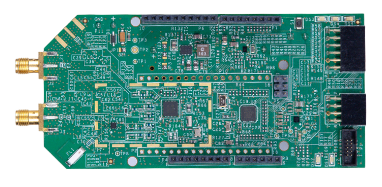
The MAX32670-LR-ARDZ base board features the MAX32670 high-reliability, ultralow power microcontroller based on Arm Cortex-M4 processor, and the LR1110 long range RF transceiver module. The integrated RF transceiver supports a frequency range from 800 MHz up to 960 MHz, making it suitable for high-performance flexible platforms that wirelessly transmit encrypted data at long-range; enabling a wide range of IoT applications using ADI sensing solutions.
This solution also utilizes Semtech’s Long Range Cloud™ Geolocation capabilities to significantly reduce power consumption by determining asset location in a cloud-based solver. Due to its low power consumption, this module is ideal for devices running on small-sized batteries The on-board MAX32670 Arm Cortex®-M4 32-bit microcontroller provides the platform with complete capability to run entire RF stacks and user applications.
Features
MCU |
|---|
Arm Cortex-M4 Core with FPU up to 100 MHz |
384 kB Flash Memory with Error Correction |
160 kB SRAM (128 kB with ECC Enabled), optionally preserved in lowest power modes |
Compatible RTC resolution for long range radio application for protocol timeout management |
Security |
Available Secure Boot |
Support cryptographic algorithms, including AES-128/192/256 |
Power |
Ultralow Power Real Time Clock with Integrated Power Switch |
With 300 nA power consumption during sleep mode |
Multi-Purpose Radio Front-End Targeting Geolocation Purposes |
GNSS (GPS/BeiDou) low-power scanning |
802.11b/g/n Wi-Fi ultralow power passive scanning |
Long Range Radio |
Support FSK, GFSK, MSK, GMSK, and Long Range FHSS modulations |
Power Output: +15 dBm transmit peak power |
Programmable bit rate up to 62.5 kbps and 300 kbps |
Support sub-GHz ISM bands from 800 MHz to 960 MHz |
High sensitivity: down to -148 dBm |
Applications
Asset location
Asset recovery
Asset traceability
Inventory management
Asset loss and theft prevention
System Architecture
Hardware Design
In order to use this base board, all hardware settings such as the hardware peripheral connections, jumpers and UART switch configurations, power configurations, connectivity options, and the USB connectors and programming connections are provided in this page. Links to the schematics and the layout files are also available below.
Components and Connections
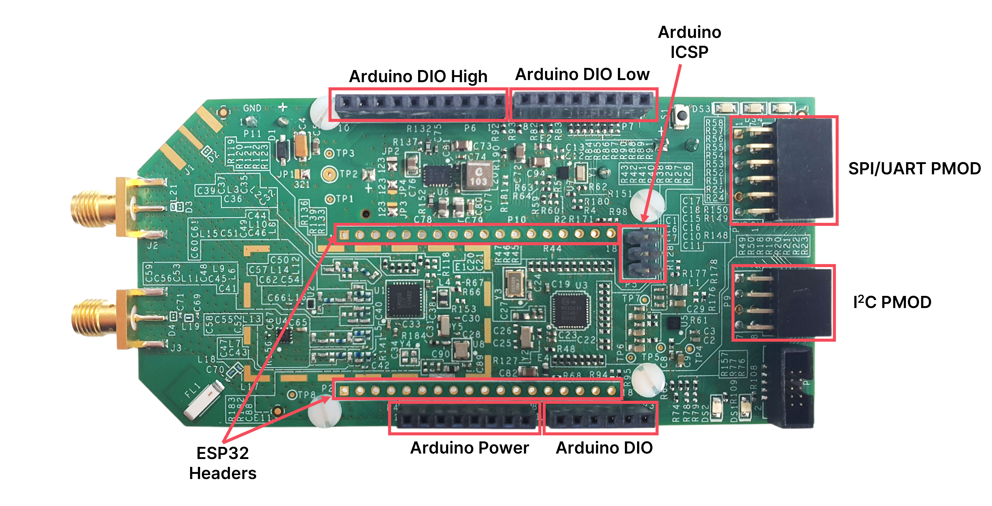
Peripheral Connectors
The following standard connectors are provided on the base board for customer to use with external add-on modules:
Connector Name |
Function |
|---|---|
DC Power Connector Header |
Input range from +4 V to +6 V DC supply voltage |
Battery Holder |
Battery holder for CR123A |
Cortex SWD Header |
Used for flash programming and debug interface; also, provides a virtual serial port connection to MAX32670 microcontroller |
PMOD_SPI |
12-pin SPI PMOD connector |
PMOD_I2C |
8-pin I2C PMOD connector |
ESP32 Connector |
ESP32 Devkit V1 connector |
Arduino Connectors |
Arduino Uno Rev3 compatible connectors |
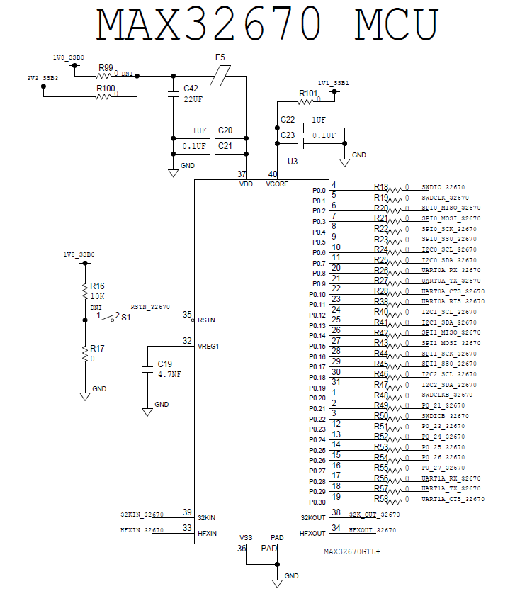
MAX32670 MCU Pin Map
The pin map for the MAX32670 MCU is described in the table and its schematic diagram below.
Net Name |
Pin |
Name |
|
UART |
|||
UART0A_RX_32670 |
20 |
P0.8 |
P0.8/UART0A_RX/I2S0_SDO/TMR0B_I |
UART0A_TX_32670 |
21 |
P0.9 |
P0.9/UART0A_TX/I2S0_WS/TMR0B_O |
UART0A_CTS_32670 |
22 |
P0.10 |
P0.10/UART0A_CTS/I2S0_SCK/TMR1B_I/DIV_CLK_OUTB |
UART0A_RTS_32670 |
23 |
P0.11 |
P0.11/UART0A_RTS/I2S0_SDI/TMR1B_O |
UART1A_RX_32670 |
17 |
P0.28 |
P0.28/UART1A_RX/TMR2D_I |
UART1A_TX_32670 |
18 |
P0.29 |
P0.29/UART1A_TX/TMR2D_O |
UART1A_CTS_32670 |
19 |
P0.30 |
P0.30/UART1A_CTS/TMR3D_I |
SPI |
|||
SPI0_MISO_32670 |
6 |
P0.2 |
P0.2/SPI0_MISO/UART1B_RX/TMR1A_I |
SPI0_MOSI_32670 |
7 |
P0.3 |
P0.3/SPI0_MOSI/UART1B_TX/TMR1A_O |
SPI0_SCK_32670 |
8 |
P0.4 |
P0.4/SPI0_SCK/UART1B_CTS/TMR2A_I |
SPI0_SS0_32670 |
9 |
P0.5 |
P0.5/SPI0_SS0/UART1B_RTS/TMR2A_O/DIV_CLK_OUTA |
SPI1_MISO_32670 |
26 |
P0.14 |
P0.14/SPI1_MISO/UART2B_RX/TMR3B_I |
SPI1_MOSI_32670 |
27 |
P0.15 |
P0.15/SPI1_MOSI/UART2B_TX/TMR3B_O |
SPI1_SCK_32670 |
28 |
P0.16 |
P0.16/SPI1_SCK/UART2B_CTS/TMR0C_I |
SPI1_SS0_32670 |
29 |
P0.17 |
P0.17/SPI1_SS0/UART2B_RTS/TMR0C_O |
I2C |
|||
I2C0_SCL_32670 |
10 |
P0.6 |
P0.6/I2C0_SCL/LPTMR0_I/TMR3A_I |
I2C0_SDA_32670 |
11 |
P0.7 |
P0.7/I2C0_SDA/LPTMR0_O/TMR3A_O |
I2C1_SCL_32670 |
24 |
P0.12 |
P0.12/I2C1_SCL/EXT_CLK2/TMR2B_I/EXT_CLK1 |
I2C1_SDA_32670 |
25 |
P0.13 |
P0.13/I2C1_SDA/32KCAL/TMR2B_O/SPI1_SS0 |
I2C2_SCL_32670 |
30 |
P0.18 |
P0.18/I2C2_SCL/TMR1C_I |
I2C2_SDA_32670 |
31 |
P0.19 |
P0.19/I2C2_SDA/TMR1C_O |
JTAG |
|||
SWDIO_32670 |
4 |
P0.0 |
P0.0/SWDIO/TMR0A_I |
SWDCLK_32670 |
5 |
P0.1 |
P0.1/SWDCLK/TMR0A_O |
SWDCLKB_32670 |
1 |
P0.20 |
P0.20/CM4_RX/TMR2C_I/SWDCLKB |
SWDIOB_32670 |
3 |
P0.22 |
P0.22/LPTMR1_I/TMR3C_I/SWDIOB |
GPIO |
|||
P0_21_32670 |
2 |
P0.21 |
P0.21/CM4_TX/TMR2C_O |
P0_23_32670 |
12 |
P0.23 |
P0.23/LPTMR1_O/TMR3C_O |
P0_24_32670 |
13 |
P0.24 |
P0.24/LPUART0_CTS/UART0B_RX/TMR0D_I |
P0_25_32670 |
14 |
P0.25 |
P0.25/LPUART0_RTS/UART0B_TX/TMR0D_O |
P0_26_32670 |
15 |
P0.26 |
P0.26/LPUART0_RX/UART0B_CTS/TMR1D_I |
P0_27_32670 |
16 |
P0.27 |
P0.27/LPUART0_TX/UART0B_RTS/TMR1D_O |
RSTN_32670 |
35 |
RSTN |
RSTN |
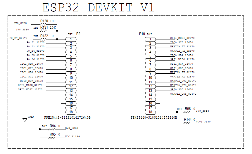
ESP32 Connector Pin Map
All connector pinouts for the ESP32 Development Board are described in the table and its schematic diagram below.
Pin Name |
Pin Number |
Pin Description |
EN |
1 |
P0_27_32670 |
GPIO |
2 |
P0_21_32670 |
GPIO |
3 |
P0_23_32670 |
GPIO |
4 |
P0_24_32670 |
GPIO |
5 |
P0_25_32670 |
GPIO |
6 |
P0_26_32670 |
GPIO |
7 |
I2C2_SDA_32670 |
GPIO |
8 |
I2C1_SCL_32670 |
GPIO |
9 |
I2C1_SDA_32670 |
GPIO |
10 |
I2C2_SCL_32670 |
HSPI CLK |
11 |
SPI0_SCK_32670 |
HSPI MISO |
12 |
SPI0_MISO_32670 |
HSPI MOSI |
13 |
SPI0_MOSI_32670 |
GPIO |
14 |
|
GPIO |
15 |
|
GPIO |
16 |
|
GND |
17 |
GND |
VIN |
18 |
VOUT_3130(def)/VCC_31334 |
VSPI MOSI |
1 |
SPI1_MOSI_32670 |
I2C SCL |
2 |
I2C0_SCL_32670 |
UART 0 TX |
3 |
UART0A_TX_32670 |
UART 0 RX |
4 |
UART0A_RX_32670 |
I2C SDA |
5 |
I2C0_SDA_32670 |
VSPI MISO |
6 |
SPI1_MISO_32670 |
VSPI CLK |
7 |
SPI1_SCK_32670 |
VSPI CS0 |
8 |
SPI1_SS0_32670 |
UART 2 TX |
9 |
UART1A_TX_32670 |
UART 2 RX |
10 |
UART1A_RX_32670 |
RTC |
11 |
UART0A_CTS_32670 |
RTC |
12 |
UART0A_RTS_32670 |
RTC |
13 |
SPI0_SS0_32670 |
RTC |
14 |
UART1A_CTS_32670 |
SDI |
15 |
|
SDO |
16 |
|
SCK |
17 |
|
3V3 |
18 |
VOUT_3130 |
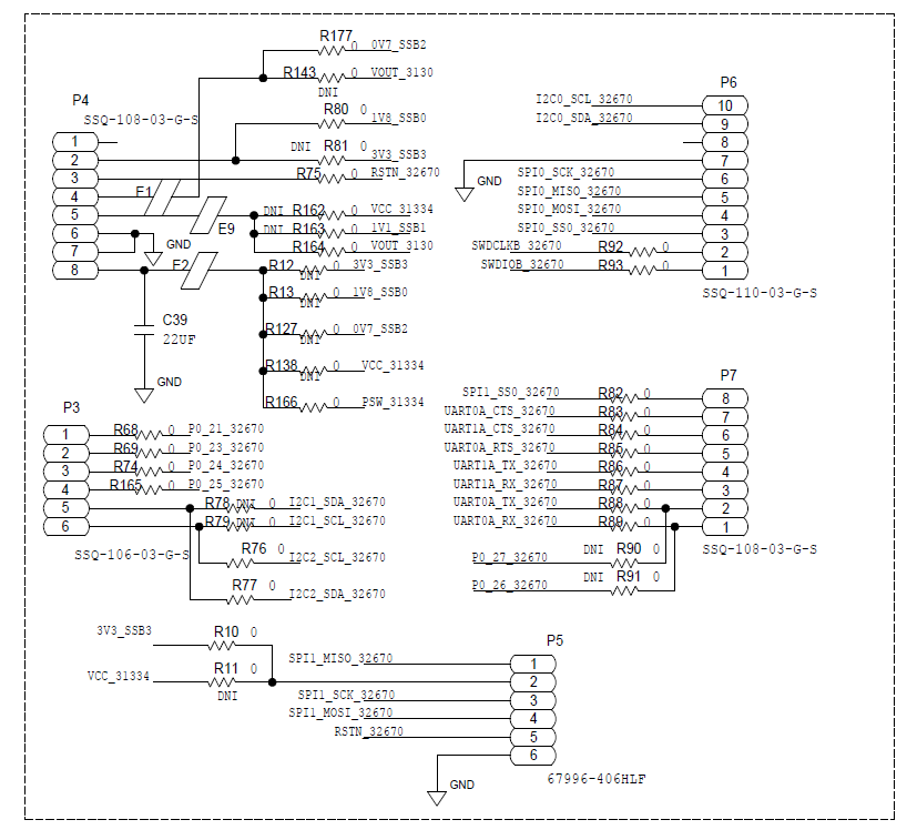
Arduino Connector Pin Map
Net Name |
Pin Number |
Pin Name |
Description |
P4 |
|||
– |
1 |
NC |
|
1V8_SSB0/3V3_SSB3(def) |
2 |
IOREF |
POW |
RSTN_32670 |
3 |
RESET |
AVR/POW |
VOUT_3130 |
4 |
3.3V |
POW |
– |
5 |
5V |
POW |
– |
6 |
GND |
POW |
– |
7 |
GND |
POW |
1V8_SSB0/0V7_SSB2/ 3V3_SSB3(def)/VCC_31334 |
8 |
VIN |
POW |
P3 |
|||
P0_21_32670 |
1 |
A0/PC0 |
AVR/DIG/ANA |
P0_23_32670 |
2 |
A1/PC1 |
AVR/DIG/ANA |
P0_24_32670 |
3 |
A2/PC2 |
AVR/DIG/ANA |
P0_25_32670 |
4 |
A3/PC3 |
AVR/DIG/ANA |
I2C1_SDA_32 670(def)/I2C2_SDA_32670 |
5 |
A4/PC4/SDA |
AVR/DIG/ANA/I2C |
I2C1_SCL_32 670(def)/I2C2_SCL_32670 |
6 |
A5/PC5/SCL |
AVR/DIG/ANA/I2C |
P6 |
|||
I2C0_SCL_32670 |
1 |
PC5/SCL |
AVR/DIG/ANA/I2C |
I2C0_SDA_32670 |
2 |
PC4/SDA |
AVR/DIG/ANA/I2C |
– |
3 |
AREF |
POW |
– |
4 |
GND |
POW |
SPI0_SCK_32670 |
5 |
PB5/SCK |
AVR/DIG/SPI |
SPI0_MISO_32670 |
6 |
PB4/MISO |
AVR/DIG/SPI |
SPI0_MOSI_32670 |
7 |
PB3/MOSI |
AVR/DIG/SPI/PWM |
SPI0_SS0_32670 |
8 |
PB2/SS |
AVR/DIG/SPI/PWM |
SWDCLKB_32670 |
9 |
PB1 |
AVR/DIG/PWM |
SWDIOB_32670 |
10 |
PB0 |
AVR/DIG |
P7 |
|||
SPI1_SS0_32670 |
1 |
PD7 |
AVR/DIG |
UART0A_CTS_32670 |
2 |
PD6 |
AVR/DIG/PWM |
UART1A_CTS_32670 |
3 |
PD5 |
AVR/DIG/PWM |
UART0A_RTS_32670 |
4 |
PD4 |
AVR/DIG |
UART1A_TX_32670 |
5 |
PD3 |
AVR/DIG/PWM/INT |
UART1A_RX_32670 |
6 |
PD2 |
AVR/DIG/INT |
UART0A_TX _32670(def)/P0_27_32670 |
7 |
PD1 |
AVR/DIG/SER |
UART0A_RX _32670(def)/P0_26_32670 |
8 |
PD0 |
AVR/DIG/SER |
P5 |
|||
SPI1_MISO_32670 |
1 |
MISO |
|
3V3_SSB3(def)/VCC_31334 |
2 |
VCC |
|
SPI1_SCK_32670 |
3 |
SCK |
|
SPI1_MOSI_32670 |
4 |
MOSI |
|
RSTN_32670 |
5 |
RESET |
|
– |
6 |
GND |
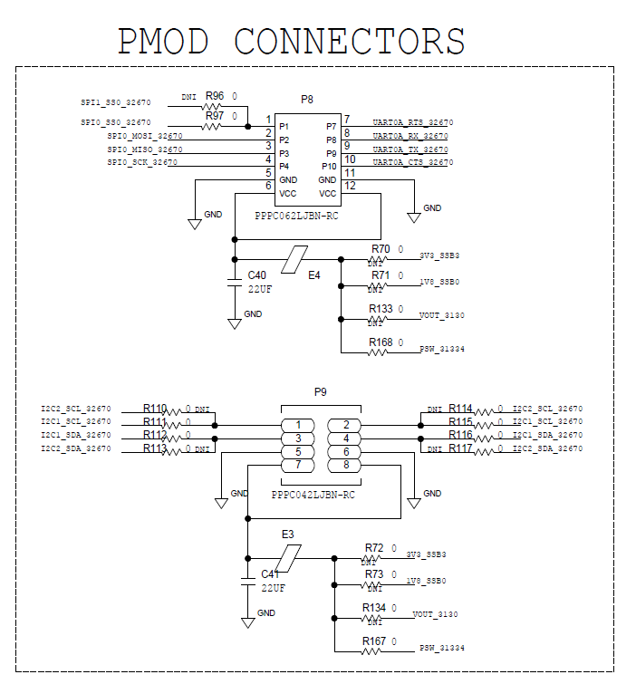
PMOD Connector Pin Map
SPI PMOD |
||
Net Name |
Pin Number |
Pin Name |
SPI0_SS0_32670(def)/SPI1_SS0_32670 |
1 |
SS |
SPI0_MOSI_32670 |
2 |
MOSI |
SPI0_MISO_32670 |
3 |
MISO |
SPI0_SCK_32670 |
4 |
SCK |
GND |
5 |
GND |
1V8_SSB3/3V3_SSB3(def)/VOUT_3130 |
6 |
VCC |
P0_21_32670 |
7 |
INT |
P0_26_32670 |
8 |
RST |
SWDIOB_32670 |
9 |
IO7 |
P0_23_32670 |
10 |
IO8 |
GND |
11 |
GND |
1V8_SSB3/3V3_SSB3(def)/VOUT_3130 |
12 |
VCC |
I2C PMOD |
||
I2C1_SCL_32670/I2C2_SCL_32670 |
1 |
SCL |
I2C1_SCL_32670/I2C2_SCL_32670 |
2 |
SCL |
I2C1_SDA_32670/I2C2_SDA_32670 |
3 |
SDA |
I2C1_SDA_32670/I2C2_SDA_32670 |
4 |
SDA |
GND |
5 |
GND |
GND |
6 |
GND |
1V8_SSB3/3V3_SSB3(def)/VOUT_3130 |
7 |
VCC |
1V8_SSB3/3V3_SSB3(def)/VOUT_3130 |
8 |
VCC |
Wireless Connectivity Options
These are the wireless connectivity options available to use for Internet of Things (IoT) applications:
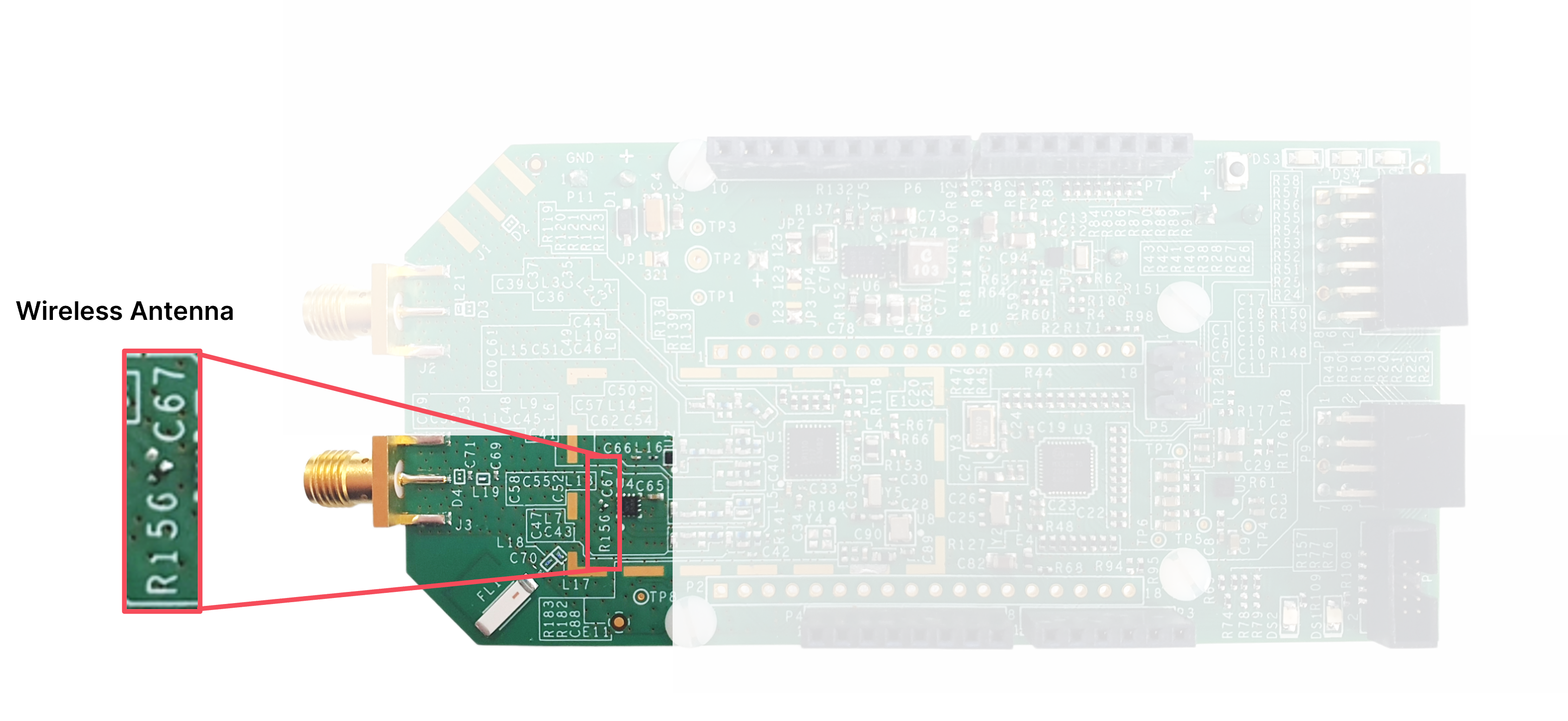
On-board Chip Antenna (FL1)
External Antenna connected through SMA connector (J3)
GNSS Antenna SMA connector (J2)
Wi-Fi Antenna SMA connector (J1)
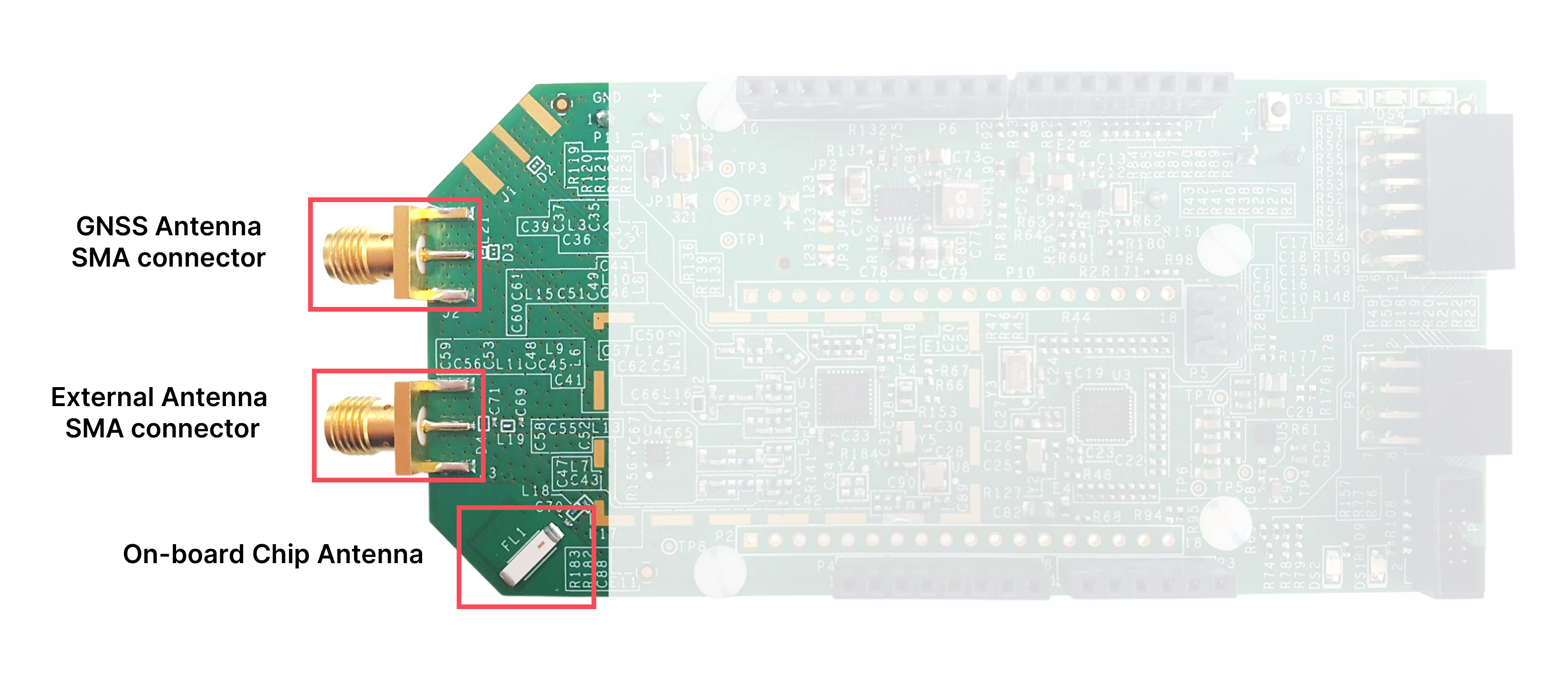
These options can be configured by populating C67 with 39 pF for the external antenna or R159 with 0 Ω for on-board RF chip antenna with the center frequency tuned at 915 MHz.
Long Range Radio Connectivity Chipset
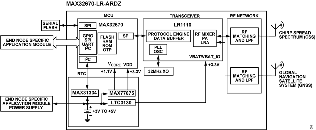
The MAX32670-LR-ARDZ utilizes the LR1110 long range radio connectivity chipset from Semtech. This chipset comes complete with the full low-power, wide area networking protocol built on top of the LoRa radio modulation technique.
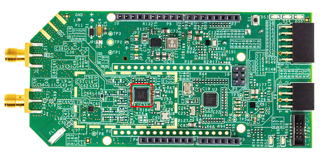
The MAX32670 communicates to the LR1110 using the SPI bus, so the users will need to send LoRa commands and data over SPI bus. Library functions calls have been specifically designed to be used with the MAX32670 and LR1110 using SPI bus.
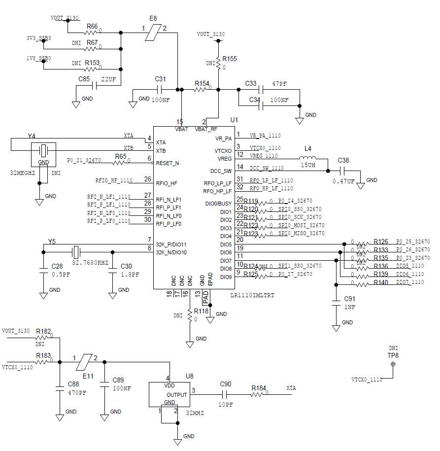
The pins that connect the MAX32670 and the LR1110 are as follows:
Connected to |
Net Name |
Pin |
I/O Name |
Function |
P0_21_32670 |
6 |
NRESET |
NRESET |
|
P0_27_32670 |
9 |
DIO9 |
IRQ |
|
SPI1_SS0_32670 |
10 |
DIO8 |
RFSW3 |
|
P0_23_32670 |
DIO7_1110 |
11 |
DIO7 |
RFSW2 |
P0_26_32670 |
DIO6_1110 |
19 |
DIO6 |
RFSW1 |
P0_25_32670 |
DIO5_1110 |
20 |
DIO5 |
RFSW0 |
SPI0_MISO_32670 |
21 |
DIO4 |
SPI MISO |
|
SPI0_MOSI_32670 |
22 |
DIO3 |
SPI MOSI |
|
SPI0_SCK_32670 |
23 |
DIO2 |
SPI SCK |
|
SPI0_SS0_32670 |
24 |
DIO1 |
SPI NSS |
|
P0_24_32670 |
25 |
DIO0/ BUSY |
BUSY |
Input Power Source Options
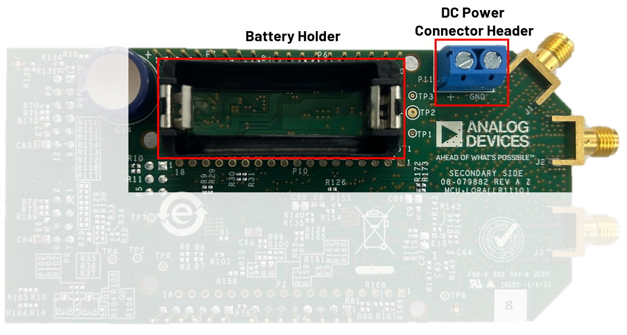
There are two (2) ways of powering the eval board, and a user may use any combination of power sources.
Terminal Block - when an external supply is connected to the Terminal block connector P11.
Battery Powered - when batteries are connected to BT1 connector on the back of the board.
Each of the different power modes, provides a different level of control and flexibility. You can find a matrix table of the different power modes and their general function here:
Power Source |
Voltage Rails Provided |
Peripherals Powered |
Function |
|---|---|---|---|
Terminal Block (P11) |
3 V to 6 V |
|
able to supply ALL voltages any peripheral might need |
Battery Power (BT1) |
3 V and 6 V |
|
able to supply ALL voltages any peripheral might need |
Reset Button
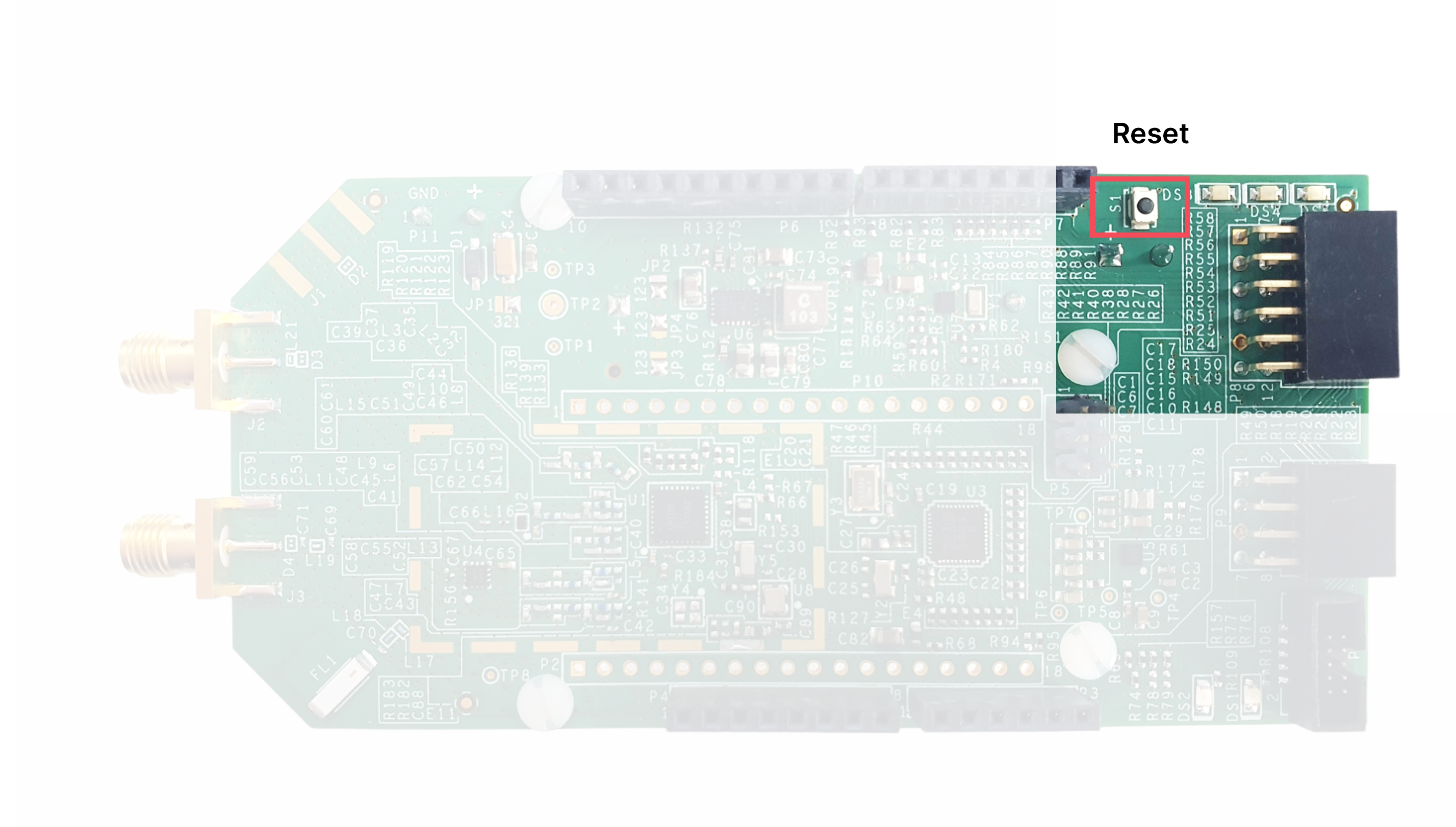
Button |
Function |
|---|---|
S1 |
provides a hardware RESET to MAX32670 microcontroller. |
LED Indicators
The base board has five LEDs: DS1, DS2, DS3, DS4, and DS5.
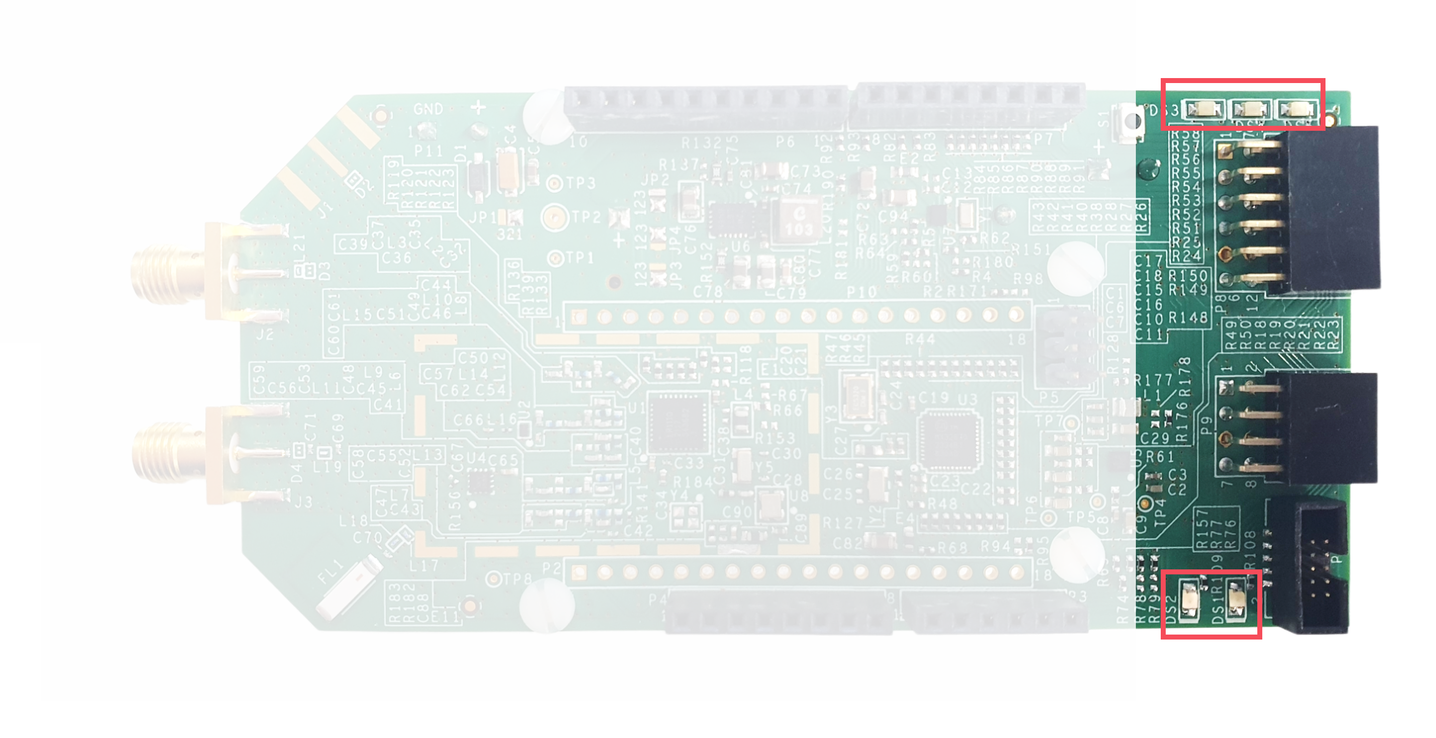
Button |
Function |
|---|---|
DS1 |
used as a LED indicator to one of the GPIOs of the MAX32670, P0.28. |
DS2 |
used as a LED indicator to one of the GPIOs of the MAX32670, P0.29. |
DS3 |
used as a LED indicator for the voltage output from the power supply. |
DS4 |
used as a LED indicator for the voltage output from the MAX31334. |
DS5 |
used as a LED indicator for the 3.3 V voltage output from the MAX3130. |
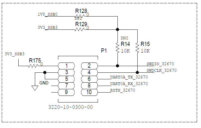
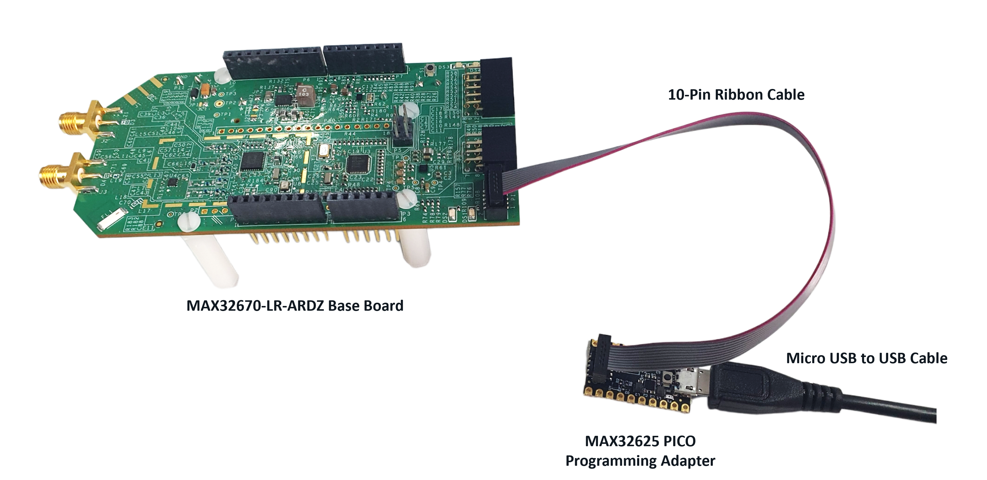
Programming Connectors
This board uses an SWD interface and the MAX32625PICO board for programming the on-board MCUs. See the MAX32625PICO page for more details.
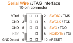
P1 - SWD interface used to program the MAX32670
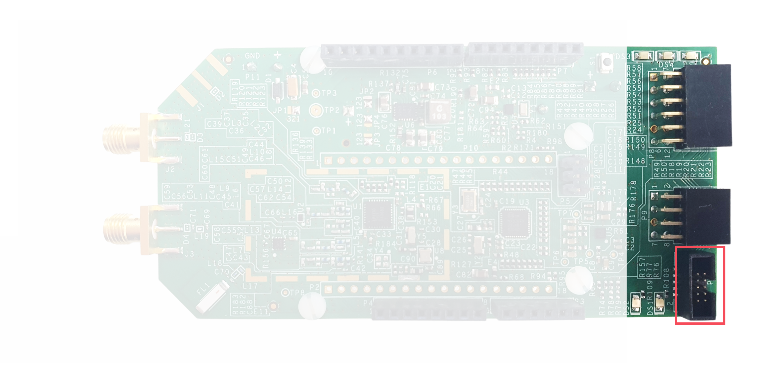
Connected to |
Pin Number |
1V8_SSB0/3V3_SSB3(def) |
1 |
SWDIO_32670 |
2 |
GND |
3 |
SWDCLK_32670 |
4 |
GND |
5 |
UART0A_TX_32670 |
6 |
7 |
|
UART0A_RX_32670 |
8 |
9 |
|
RSTN_32670 |
10 |
The connector used are based off the 10-pin Arm Cortex standard pinout (0.05” pin spacing). That pinout is common to both JTAG and SWD debug modes and is depicted in the following image.
The debugger board will need to be plugged in via the USB port in order to program any board.
In order to program the MAX32670 node board, the board must be powered by (1) CR123A battery or by an external power supply through P11. Otherwise, there will be no connection between the two boards. </WRAP>
System Setup
PHASE 1: Hardware Setup
Note that this setup only applies for MAX32670-LR-ARDZ Base Board. Users may use a different base board or microcontroller, however the firmware built for this demo application cannot be used as this is specifically designed for the MAX32670-LR-ARDZ.
Equipment Needed
One (1) MAX32670-LR-ARDZ Base Board
One (1) EV-CATTLETAG-ARDZ Sensor Node
One (1) MAX32625PICO Rapid Development Platform with 10-pin ribbon cable with firmware image: MAX32625PICO Firmware Image for MAX32670
One (1) CR123A Battery or any equivalent external DC power supply (+3V to +4.7V) Note that this is not included in the kit
One (1) Micro USB to USB cable
Host PC (Windows 10 or later)
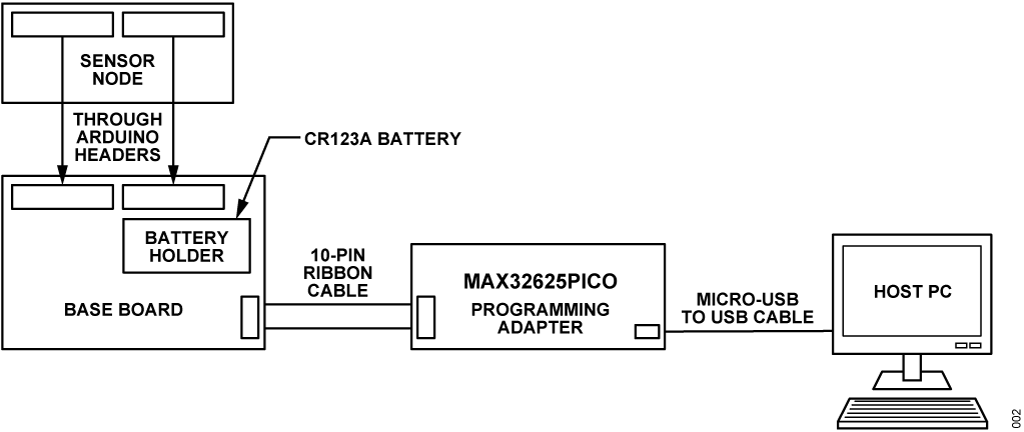
Insert one CR123A battery (3V to 4.7V) into the battery holder (BT1 connector) of the MAX32670-LR-ARDZ Base Board.
Make sure to check for the battery polarity in the BT1 connector, refer to the figure below. The DS3 LED will light up indicating that you have inserted the battery correctly and that power is provided in the base board.
Connect the EV-CATTLETAG-ARDZ Sensor Node to the MAX32670-LR-ARDZ Base Board by aligning the corresponding Arduino headers on each board.
Connect the MAX32625PICO programming adapter to the MAX32670-LR-ARDZ Base Board through the 10-pin ribbon cable.
Make sure that the MAX32625PICO programming adapter has been flashed with the correct image before connecting it to the MAX32670-LR-ARDZ Base Board. If you do not know how to load the image, click on the instructions below:
How to flash the firmware image in the MAX32625PICO
Download the firmware image: MAX32625PICO Firmware Image for MAX32670
Do not connect the MAX32625PICO to the MAX32670-LR-ARDZ Base Board yet.
Connect the MAX32625PICO to the Host PC using the micro USB to USB cable.
Press the button on the MAX32625PICO. (Do not release the button until the MAINTENANCE drive is mounted).
Release the button once the MAINTENANCE drive is mounted.
Drag and drop (to the MAINTENANCE drive) the firmware image.
After a few seconds, the MAINTENANCE drive will disappear and be replaced by a drive named DAPLINK. This indicates that the process is complete, and the MAX32625PICO can now be used to flash the firmware of the MAX32670-LR-ARDZ Base Board.
Connect the MAX32625PICO programming adapter to the Host PC using the micro USB to USB cable.
Once you have completed this setup, proceed to PHASE 2 found in ADI Long Range Wireless Radio Software User Guide.
Resources
Design and Integration Files
Download
MAX32670-LR Design Support Package Rev. C
Schematic
Bill of Materials
Layout
Allegro Project
Help and Support
For questions and more information about this product, connect with us through the Analog Devices Engineer Zone.