Jupiter SDR Hardware Overview
Processing System
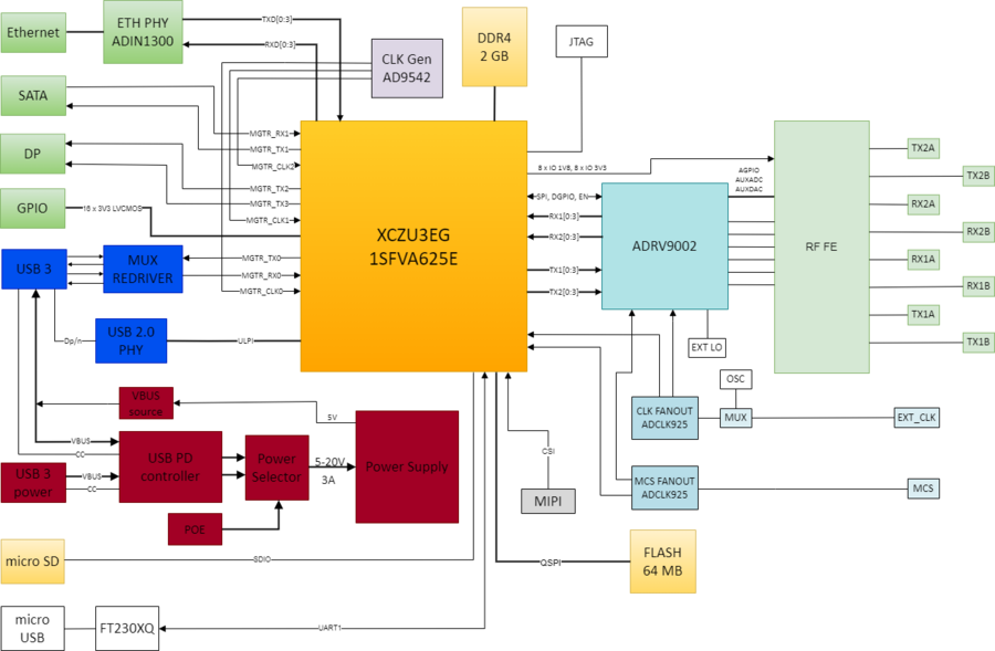
Zynq Ultrascale+ MPSOC XCZU3EG
Application Processing Unit - Quad ARM Cortex-A53 (1.5 GHz each)
L1 Cache 32KB I / D per core
L2 Cache 1MB
256kB on-chip Memory
Real time Processing Unit - Dual ARM Cortex-R5 (600 MHz each)
L1 Cache 32KB I / D per core
128kB/core memory
Graphics Processing Unit - ARM Mali-400 MP2
L2 Cache 64KB
Programmable logic
154k Logic cells
360 DSP slices
7.6Mb block RAM
DDR
2GB DDR4 with 32 bit data bus connected to the PS of XCZU3EG are shared by the OS, video (optional) and RF data streaming. XCZU3EG DDR memory controller has the maximum data rate limited to 2133Mbps.
Configuration and boot
The following boot options are supported:
Quad-SPI - 2 x 64MB Flash memory
dual parallel configuration with 8-bit data bus width
32 bits addressing
ZU3EG boot mode configuration MODE[3:0] = 0010
SD1 LS (3.0)
Supports FAT 16/32 filesystem
ZU3EG boot mode configuration MODE[3:0] = 1110
MODE pins are automatically configured in hardware so that the SD card boot option has higher priority than Quad-SPI Flash.
The ZU3EG on-chip SD Controller is compatible with SD memory card specification version 3.01, supporting UHS-I speeds and SDXC capacity format. The front panel includes a micro SD card connector.
Multi Gigabit Transceiver (MGTR)
XCZU3EG Zynq Ultrascale+ has 4 GTR channels up to 6Gb/s. The following table shows the GTR channels usage on Jupiter SDR.
MGTR Channel |
Interface |
Data Rate |
|---|---|---|
RX0 |
USB3 |
USB 3, 5Gb/s |
TX0 |
USB3 |
USB 3, 5Gb/s |
RX1 |
SATA |
SATA III, 6Gb/s |
TX1 |
SATA |
SATA III, 6Gb/s |
RX2 |
||
TX2 |
DP |
DP1 v1.2, 5.4Gb/s |
RX3 |
||
TX3 |
DP |
DP0 v1.2, 5.4Gb/s |
CLK0 |
USB3 |
26 MHz |
CLK1 |
DP |
108 MHz |
CLK2 |
SATA |
150 MHz |
CLK3 |
not used |
AD9542 provides a flexible solution for generating the required MGTR clocks. It integrates a dual PLL with 5 pairs of clock output pins. AD9542 is capable to load its configuration from EEPROM making it suitable for stand alone use.
User Interfaces
USB
USB Type-C data connector exposes a DRP (Dual Role Port) USB 3.1 Gen1 interface which operate as either a DFP (Downstream Facing Port) or a UFP (Upstream Facing Port):
UFP – it is used to connect Jupiter-SDR (device) to a computer (host) for data streaming
DFP – it is used to connect different USB3 devices to Jupiter-SDR (keyboard, mouse, wi-fi, etc.);
backward compatibility with USB2 interface is supported by USB3320 transceiver connected over ULPI interface to the PS side of XCZU3EG.
Ethernet
ADIN1300 is a 10BASE-Te/100BASE-TX/1000BASE-T IEEE 802.3 compliant Ethernet PHY interfaced to the PS of XCZU3EG through RGMII interface.
SATA
XCZU3EG supports SATA III – 6Gb/s or 600MB/s. SATA interface is exposed to the user through an eSATA connector which supports 2.5K mating cycles and shielded cable.
Display Port
XCZU3EG supports Display Port 1.2 source-only controller with two lanes having link data rate of 1.62Gb/s, 2.7Gb/s or 5.4Gbps. Most of the monitors will achieve 1080p at 60 FPS. It also supports AUX channel for audio digital signal transfer (720 Mb/s).
Warning
AMD Xilinx provide a list of monitors that were tested and work with the Ultrascale+ Display Port controller.
Debug interfaces
Micro USB connector exposes an UART interface that gives the possibility to communicate with Linux running on the XCZU3EG. The FT230XQ transceiver is used for USB to UART interfacing.
Optionally the user could populate 14 pins JTAG header inside the enclosure that allows to do deeper development debug.
GPIOs
We are exposing XCZU3EG IO lines of Bank 26 to a 20 pins (1.27mm pitch) header on the front panel. The GPIO connector also provide 3.3V supply rail to the user which is also used to supply the FPGA IO Bank.
16 lines independently configurable as inputs or outputs
3V3 TTL levels
ESD protection
I2C0, SPI0, UART0 could be exposed using EMIO
RF Front-end
The Main Board RF front end block diagram is presented in the following picture.
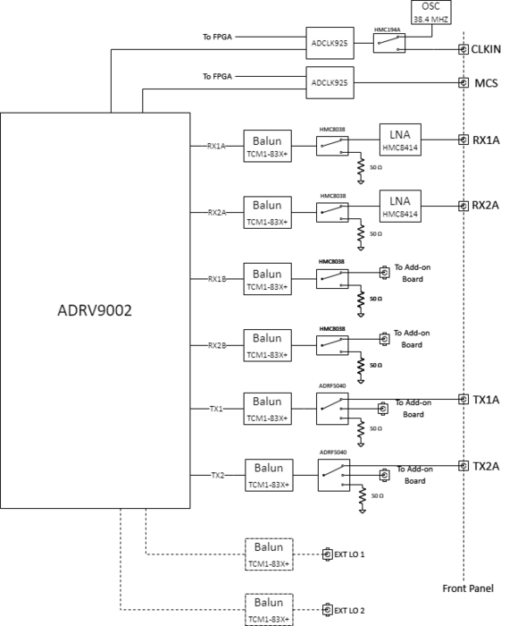
ADRV9002 clock
Jupiter SDR supports two ADRV9002 clock sources:
on-board 38.4MHz oscillator - GTXO-74V/JI made by Golledge
external clock input exposed to the dedicated SMA connector
50 ohm input
input level range from -8dBm to 15.8 dBm
adrv9002_clksrc signal selects ADRV9002 clock source:
LOW - on-board oscillator (default)
HIGH - external clock
The adrv9002_clksrc control is implemented in the device tree.
The on-board oscillator GTXO-74V is coming with voltage tune feature that allows frequency adjustment in the range of +/-8 to +/-14 ppm. The oscillator has frequency tuning pin connected to AUXDAC3 of ADRV9002 which allows frequency correction algorithms to tune the LO frequency. The following formula could be used to find required DAC voltage for desired tune voltage:
For example if we want VTUNE = 1.5V then we need VAUXDAC3 = 0.659V.
RF FE Main Board
The main board expose to the front panel two wide band receive channels RX1A and RX2A which are connected to the ADRV9002 transceiver Rx A channels. The receive path consist of a by-passable LNA HMC8414, a non-reflective SPDT switch HMC8038 that allows to terminate with 50 ohms the RX input during internal calibration and a TCM1-83X+ MiniCircuits balun. The control of calibration switch is done by the driver and is not exposed to the user. The frequency range of the main board RX1A and RX2A paths is 100 MHz to 6 GHz.
On the main board we have another two receive channels RX1B and RX2B which are connected to Rx B channels of ADRV9002. These receive channels are connected to the RF add-on board through uFL cables and also have the same SPDT switch and balun as on the RX A channels.
The main board also expose to the front panel two transmit channels TX1A and TX2A which consists of a TCM1-83X+ balun and a three way non-reflective switch ADRF5040 which allows disconnecting the TX output during internal calibration or connecting the transmit path to the RF Add-on board. There are some attributes exposed to the user that allows selecting between TX1A and TX1B respective TX2A and TX2B. (link to command example)
RF FE Add-on board
The picture below show the block diagram of the RF Add-on board.
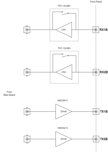
The RF Add-on board expose B receive channels RX1B and RX2B to the front pannel. The receive path has a by-passable LNA TSY-13LNB+ with frequency range 10MHz to 1GHz.
TX1B and TX2B channels include just an amplifier HMC8413 that boosts by 20 dB the transmit signal.
RF FE Add-on interface
Main Board expose a control interface for the RF Add-on board to a 40 pin connector. The table below show the pinout of the interface connector.
VAGPIO_1P8 |
1 |
2 |
ADV9002_AUXADC_0 |
ADV9002_AUXADC_1 |
3 |
4 |
ADV9002_AUXADC_2 |
ADV9002_AUXADC_3 |
5 |
6 |
ADV9002_AUXDAC_0 |
ADV9002_AUXDAC_1 |
7 |
8 |
|
ADV9002_AUXDAC_3 |
9 |
10 |
GND |
ADV9002_AGPIO_5 |
11 |
12 |
ADV9002_AGPIO_7 |
ADV9002_AGPIO_8 |
13 |
14 |
ADV9002_AGPIO_9 |
ADV9002_AGPIO_10 |
15 |
16 |
ADV9002_AGPIO_11 |
3V3 |
17 |
18 |
GND |
IO_L9P_AD3P_26 |
19 |
20 |
IO_L10P_AD2P_26 |
IO_L9N_AD3N_26 |
21 |
22 |
IO_L10N_AD2N_26 |
IO_L11P_AD1P_26 |
23 |
24 |
IO_L12P_AD0P_26 |
IO_L11N_AD1N_26 |
25 |
26 |
IO_L12N_AD0N_26 |
1V8_VCCO |
27 |
28 |
GND |
IO_L1P_T0L_N0_DBC_64 |
29 |
30 |
IO_L2P_T0L_N2_64 |
IO_L1N_T0L_N1_DBC_64 |
31 |
32 |
IO_L2N_T0L_N3_64 |
IO_L21P_T3L_N4_AD8P_64 |
33 |
34 |
IO_L23P_T3U_N8_64 |
IO_L21P_T3L_N5_AD8N_64 |
35 |
36 |
IO_L23N_T3U_N9_64 |
VIN_PWR |
37 |
38 |
GND |
VIN_PWR |
39 |
40 |
GND |
Transceiver Resources
4 AUX ADC channels
4 AUX DAC channels
6/10 AGPIO lines (AUX DAC channels could also be used as AGPIOs)
FPGA Resources
8 FPGA IO LVTTL 3V3 (HD bank)
8 FPGA IO LVTTL 1V8 (HP bank)
Power Budget
VAGPIO_1P8 - 1V8/100 mA
3V3/100 mA
VIN_PWR - 5V - 20V/TBD A
The user could build their own RF Add-on board to suit their specific needs.
RX gain control
ADRV9002 external gain control functionality allows AGPIO pins configured as output to automatically set required front end gain. The software exposes required attributes that allows to manually control the AGPIO state. (link to command example)
LNA control |
ADRV9002 external gain control |
|---|---|
RX1A |
agpio4 |
RX1B |
agpio5 |
RX2A |
agpio6 |
RX2B |
agpio7 |
AGPIO driven LOW bypass the LNA while driven HIGH turns on the LNA.
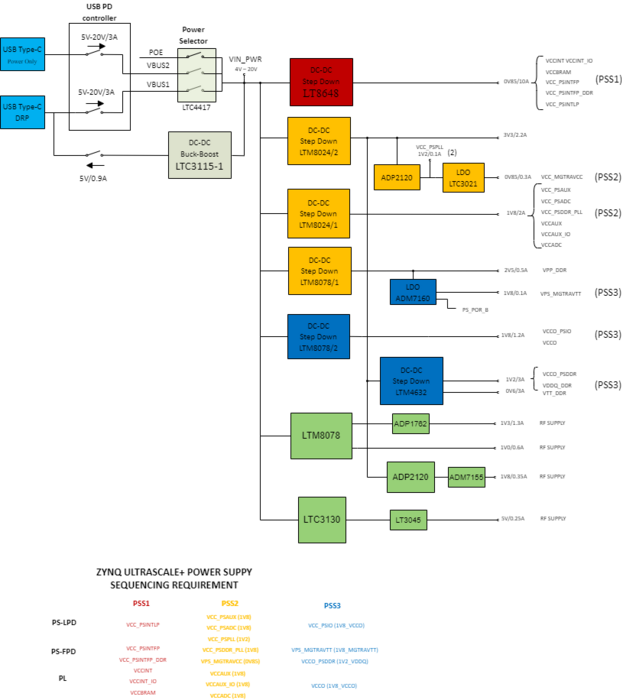
Power
The picture below show the power supply high level block diagram.
Power Sources
The board has three power sources:
USB Type-C (power only) - priority 1
power sink - PDO1 9V/3A (default), PDO2 5V/3A
USB Type-C (data and power) - priority 3
power sink - PDO1 5V/3A
power source - PDO1 5V/0.9A
POE - priority 2
LT4276 - IEEE 802.3at 25.5W Compliant
LTC4417 power selector turns on the highest priority valid power source. The switchover from one power source to another should not cause the board to reset when total power consumption of the system does not exceed 15W.
Warning
When you want to use Jupiter SDR by just connecting one cable to the USB Type-C data and power port make sure that your computer’s USB port (or docking station) supports 5V and 3A PDO. Jupiter SDR will not boot up with 5V and 1.5A PDO.
Warning
The board is not going to power up if your PSE (Power Source Equipment) does not support POE+ (IEEE 802.3at).
System Power on/off
LTC2955 is a push button on/off controller that manages the power supply enable/disable when the push button is pressed. A short button press will generate an enable signal to the power selector which is enabling the appropriate path and the board powers up. Once the board has booted up a short press of the button will notify the operating system that power off is desired then when operating system is ready it will send the shutdwon signal to the push button controller which in turn will disable the power selector cutting off the power of the board. When things are not working as expected it is possible to force a shutdown by pressing the button more than 5s.
System Monitoring
LTC2945 measures the input voltage and current consumption of the entire board giving the board’s total power consumption.
ZU3EG and ADRV9002 integrated temperature sensors offers the possibility to monitor system’s hottest parts.
Fan control
The fan could be controlled to be in three states: off, low speed and high speed. There are two lines that control the fan speed:
fan_en - enables the fan to spin
fan_ctl - when the fan is enabled the signal controls the fan speed to low speed or high speed.
fan_en |
fan_ctl |
fan state |
|---|---|---|
LOW |
LOW |
off |
LOW |
HIGH |
off |
HIGH |
LOW |
low speed |
HIGH |
HIGH |
high speed |
By default the fan is set to low speed. For higher power applications the fan can be set to high speed by changing the device tree configuration.
Mechanical
Jupiter SDR temperature storage and operating range is 0 to 50 degC.
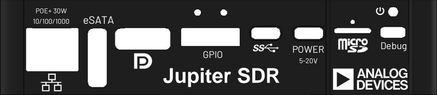
Panels Map
The early samples doesn’t have the panels printed. We are presenting in the next pictures the meaning of each connector exposed on the two sides of the enclosure.