Ethernet-APL Considerations
Surge Protection
Ethernet-APL specifications requires the use of 25A surge protection devices to avoid damage due to fast transients. To fulfill this requirements a 25A TVS diode is needed. Due to the parasitic capacitance of this component (D3), it is important to implement a low capacitance diodes bridge (D26 to D29) to minimize the TVS diode capacitance to guarantee proper Ethernet communication.
In addition, due to the voltage generated by the TVS diode, it is important to protect the ADIN1110 Tx pins. To achieve this requirement, a second pair of TVS diodes (D15 and D16) has been included in these pins.
Power-up Requirements
To guarantee that the connection of a new device into the field switch won’t impact other devices connected to the same field switch, there are mandatory power-up requirements:
Maximum current step must be <50mA
Maximum di/dt of 10mA/ms
Maximum charge of 20μJ
No more than 6 current events during the first second
After the first second the maximum di/dt is limited to 10mA/ms.
More details can be found in APL Port Profile Specification or the IEC TS 63444 standard.
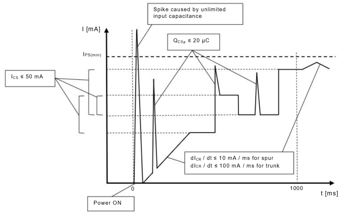
Figure 1 Illustrative Current Step Characteristics During Power-up
There is sequencing implemented on the power circuit of the APL field device; the power parts should never start-up at the same time such that it will cause huge spike that violates the APL specifications or even cause malfunction if it is not design as intended.
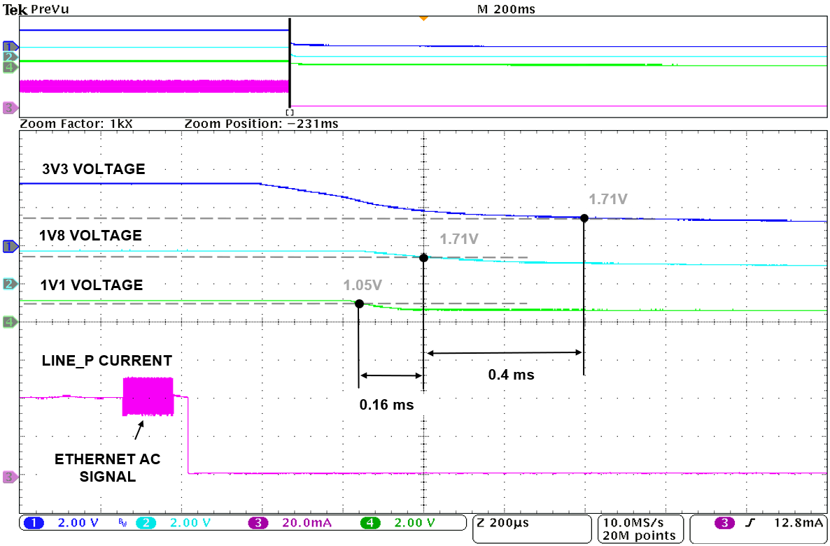
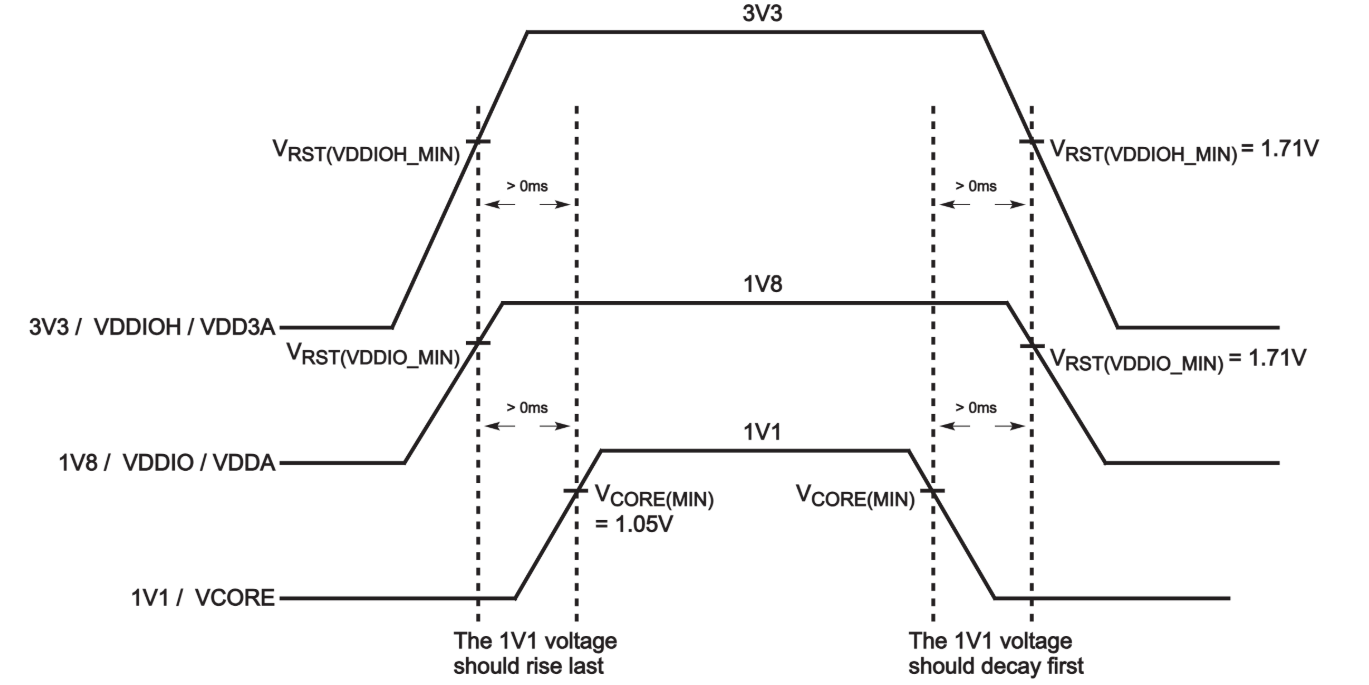
In addition, a proper power sequence is necessary for the microcontroller MAX32690, this is for the sequence specific for the following voltage lines of the microcontroller’s main supply pins: 3V3 (VDDIOH/VDD3A), 1V8 (VDDIO/VDDA) and 1V1 (VCORE). It is recommended that at least every voltage signal rise has a sequence in which have a time distances apart, either to the time difference between amplitude, or more specifically, the time difference between the minimum or threshold/reset voltages of the three main supply pins of MAX32690: VRST(VDDIOH_MIN) = 1.71V, VRST(VDDIO_MIN) = 1.71V and VCORE(MIN) = 1.05V.
In power-up capture of the LINE_P current along with the voltages of REG_3V5, SUP_3V3 and ISO_3V3 one main observation is that the spikes are generated during the beginning of conduction of every voltage regulator (e.g., LDO and Buck Converter). If there is no power sequencing, all of these parts might start-up at the same time, failing the charge requirement on the spike from the large peak current it might generate, and may cause other failures on the reference design.
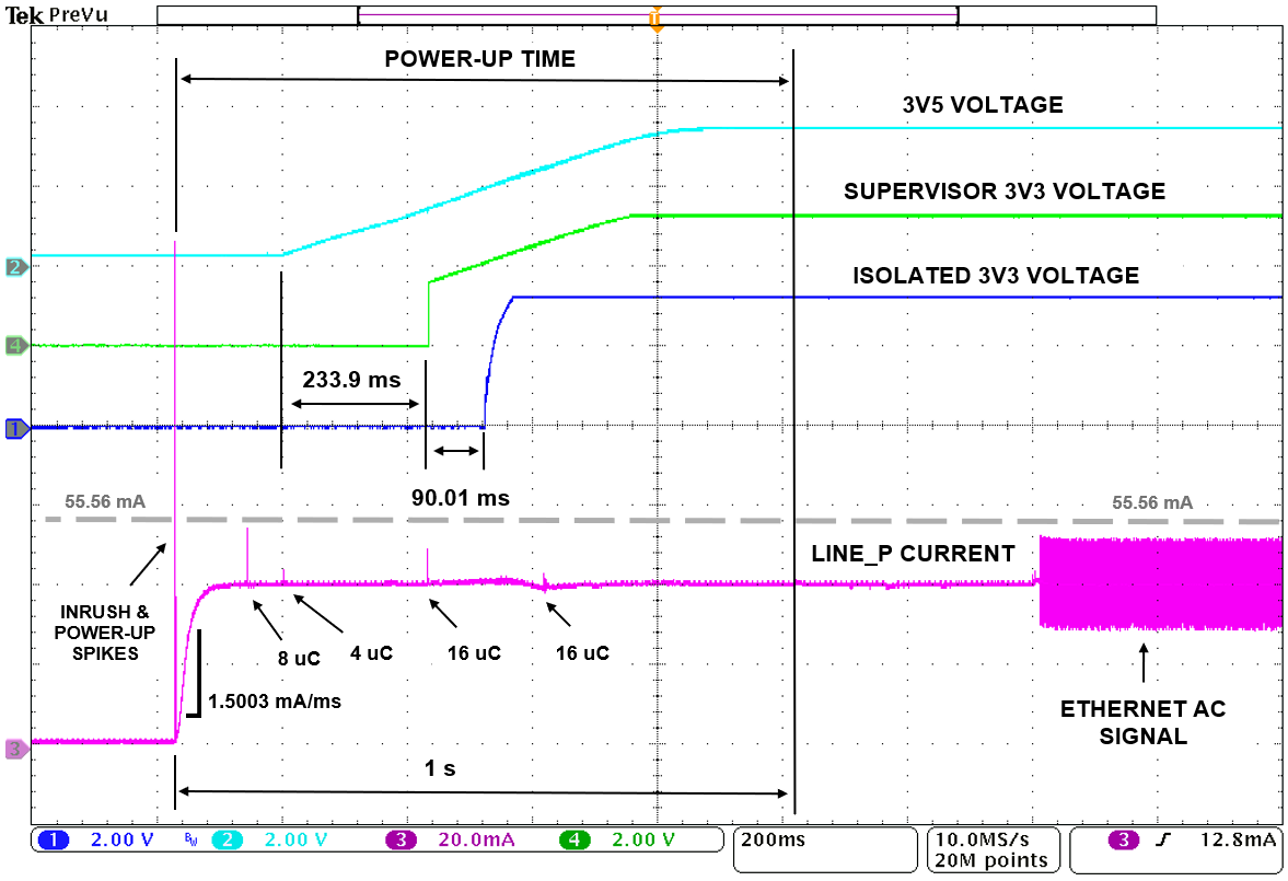
Figure 3 Hot Input LINE_P Current Capture w/ REG_3V5, SUP_3V3, ISO_3V3 Voltages
There is another power-up capture, in which the line current is captured along with the LINE_P voltage and the LOAD_P voltage shown in below figure. During hot plugging scenario, the LINE_P voltage rise is extremely fast which generate the main inrush, and this is to be expected. The inrush does not necessarily have to pass the 20uC charge maximum, but it is still measured to see and prove that even at very high peak, the charge is small granted that it happened too fast. The critical events of current however, are the spikes that happened after the inrush along with the di/dt.
Looking at Figure 3, the start-up or di/dt slope or slew rate is only at 1.5003 mA/ms which is slow enough and it didn’t violate the SPUR di/dt maximum of 10mA/ms. None of the spikes happening after the inrush has a charge value violating the 20μC maximum. In addition to the charge and di/dt, the amplitude of all the “events” which are the spikes and steps of the line current should not exceed the maximum amplitude feasible, which is dictated on its power specification, which for Power Class A, the maximum value should never exceed 55.56mA. The reference design has passed the APL port profile current step characteristics requirement for start-up during hot-plug scenario.
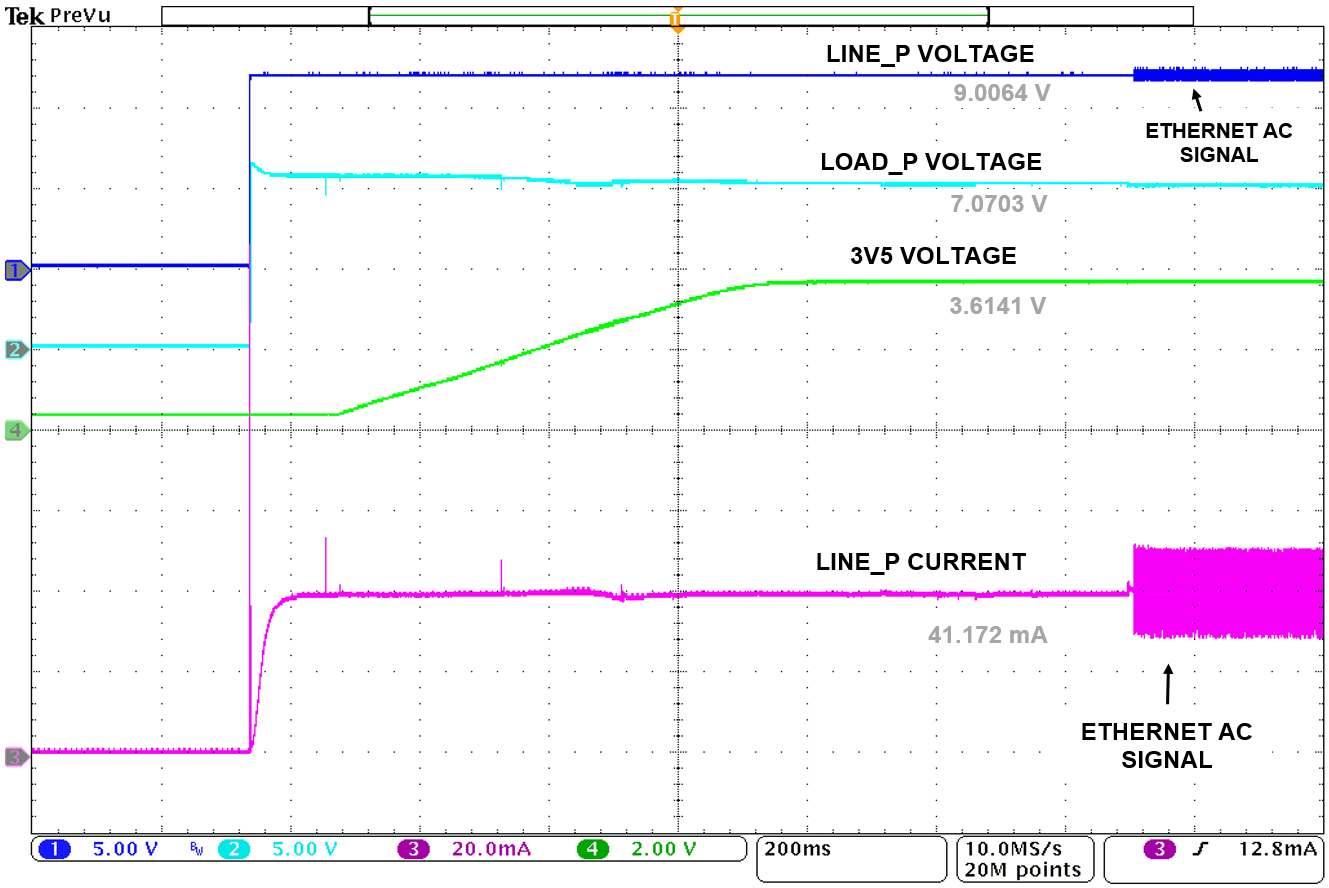
Figure 4 Hot Input LINE_P Current Capture with REG_3V5, LINE_P, LOAD_P Voltages
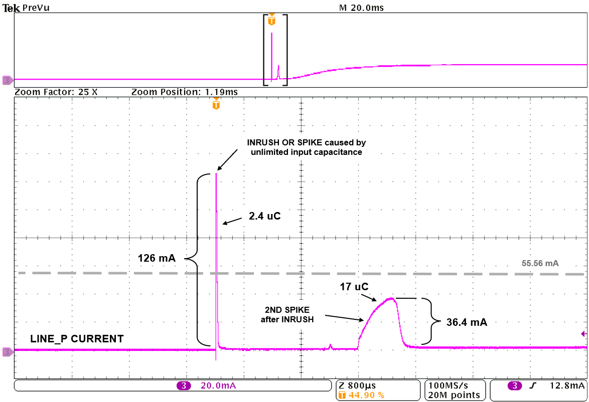
Zooming in the beginning of the power-up sequence the following are measured: The inrush only has a 2.4μC of charge despite the high peak current of 126mA because of its very fast time, take note that the inrush doesn’t require to pass the 20μC. The more critical spike is the one happening after the inrush which has a charge of around 13μC to 17μC with a peak of 36.4mA but has a wider time on the spike. To optimize the 2nd Spike, it is recommended to have a very small shunt capacitance in the load side of LT8440 or the LOAD_P node, the lower the capacitance, the lower the spike peak will be and the shorter the charging time, thus reducing the spike’s effective charge.
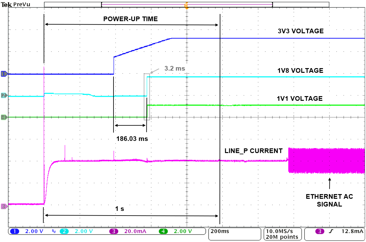
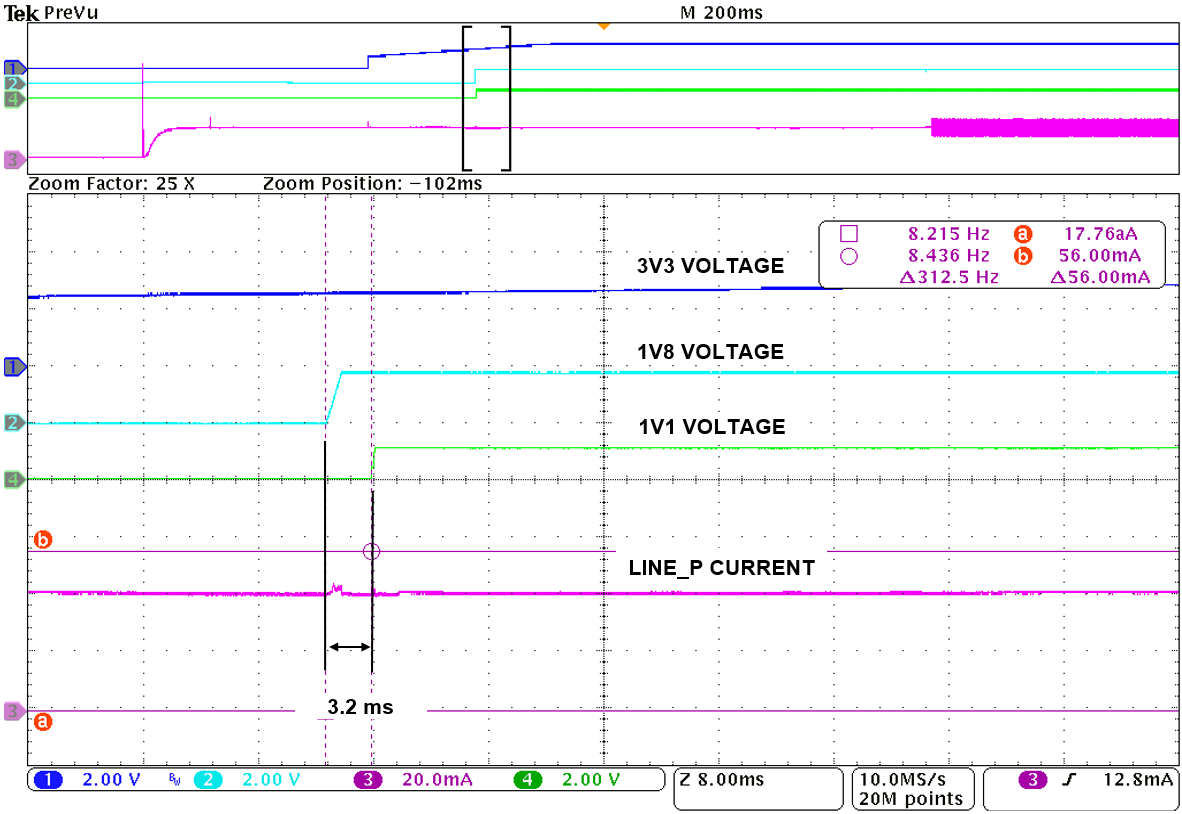
For the same power sequence during power-up, the LINE_P current is capture along with the primary three supply voltages of the signal chain: 3V3, 1V8 and 1V1. The time distance between 3V3 and 1V8 is 186.03ms, between 3V3 and 1V1 is 189.23ms, and zooming in further, the time distance between 1V8 and 1V1 is 3.2ms. The sequence is in correct order for start-up, which is 3V3 first, 1V8 second and 1V1 third or last.
The capture for the power shut down sequence of LINE_P current and the main three supply voltages for the microcontroller, following the threshold or the minimum reset voltages of each supply: The time between 3V3 (min = 1.71V) and 1V8 (min = 1.71V) is 0.4ms, between 3V3 (min = 1.71V) and 1V1 (min = 1.05V) is 0.56ms and between 1V8 (min = 1.71V) and 1V1 (min = 1.05V) is 0.16ms. It is also following the correct sequence for shutdown being 1V1 first, 1V8 second and 3V3 third or last.