Hardware User Guide
I/O Voltage
The AD-FMCOMMS3-EBZ (AD9361) assumes a VDD_INTERFACE voltage between 1.71 V and 2.625 V (1.8 to 2.5 +/- 5%), so on your FPGA carrier board, you should ensure that VADJ is between these levels. Setting things to 3.3 V will damage the part.
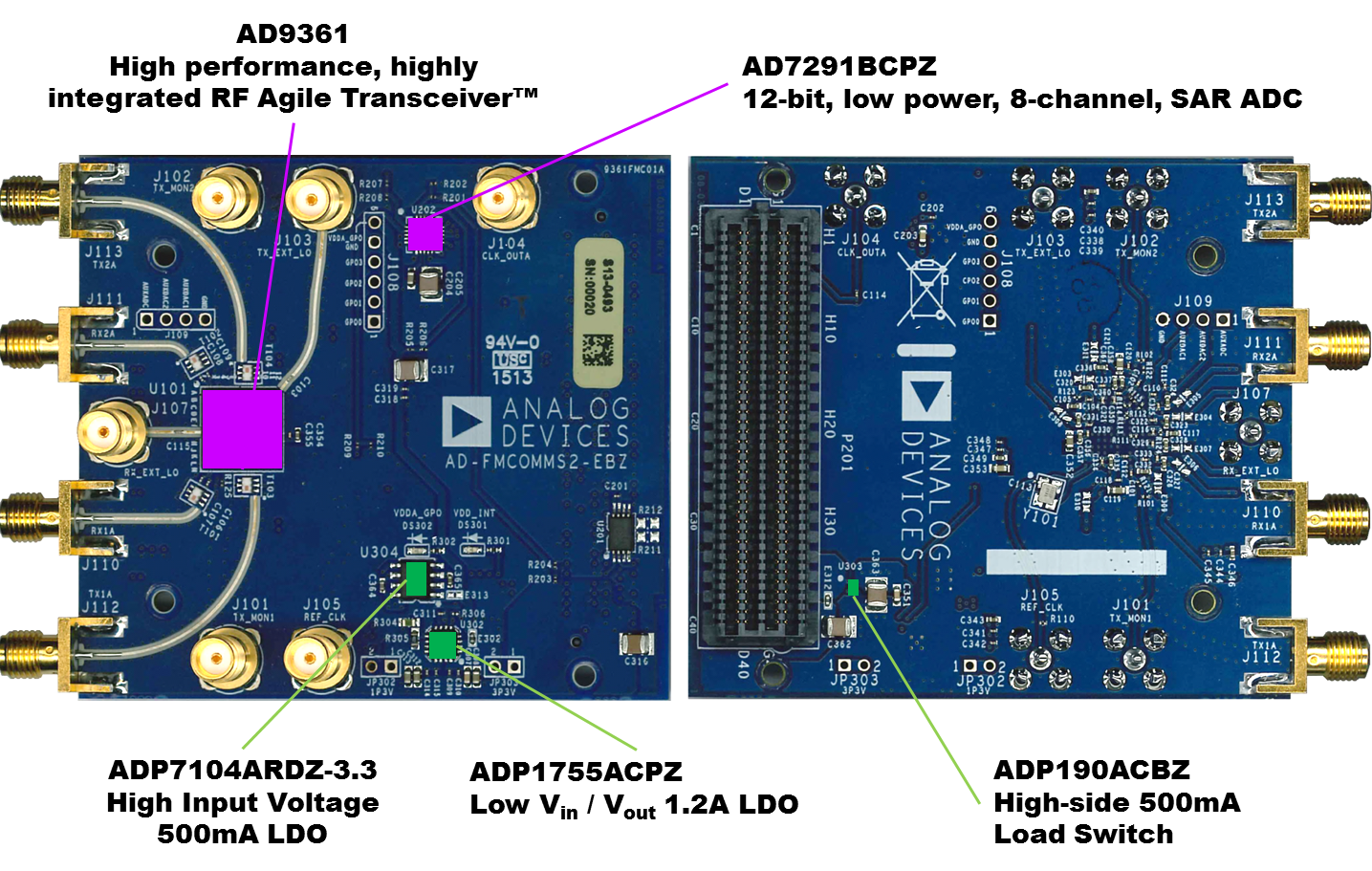
Picture and Main components
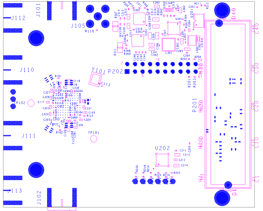
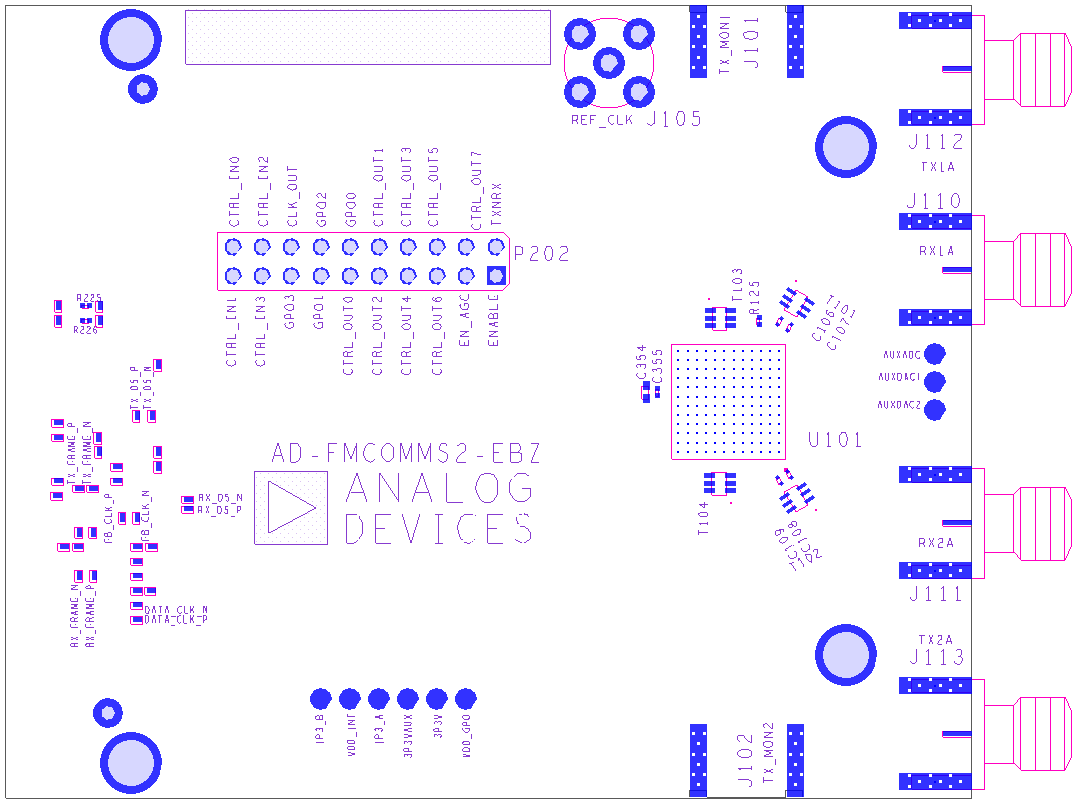
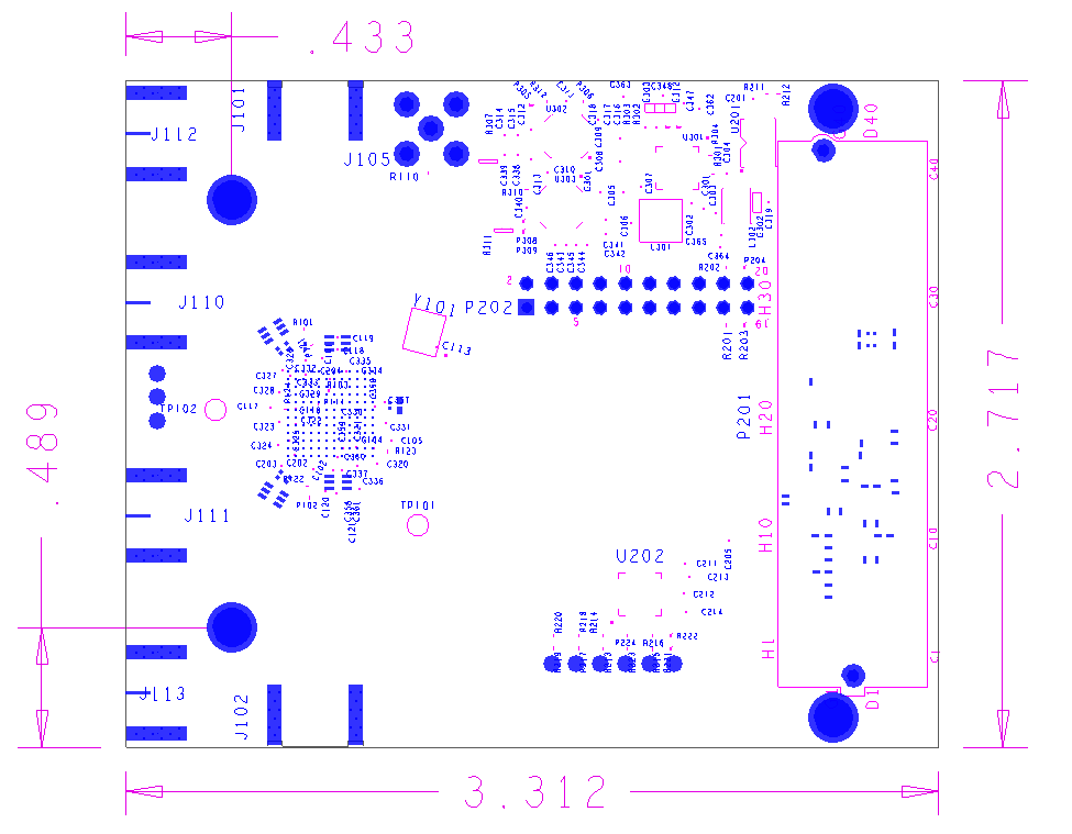
Outline
For those that don’t want to load up the Allegro viewer, here is a basic outline/component placements of the board. While this board does meet parts of the VITA-57.1 (FMC) specifications, there are many things it violates, and is not designed to be a form/fit/function board.
The FMC cutout for the bezel is missing (so we could space the SMA connectors out as far as possible, and achieve maximum isolation between the channels.
The mounting holes near the end of the board with the connectors is also in the wrong place (so it didn’t effect the RF path between the connectors and the AD9361.
The FMC height specification on the top side of the board is violated to put some 90 degree SMA connectors.
Size
The size of the board (not including the SMA connectors, which project beyond the edge of the board) is 73.3mm x 69mm. This is under the FMC specifications of 84mm x 69mm). The mounting holes are not compliant with the FMC standard, and are shown below.
Layers
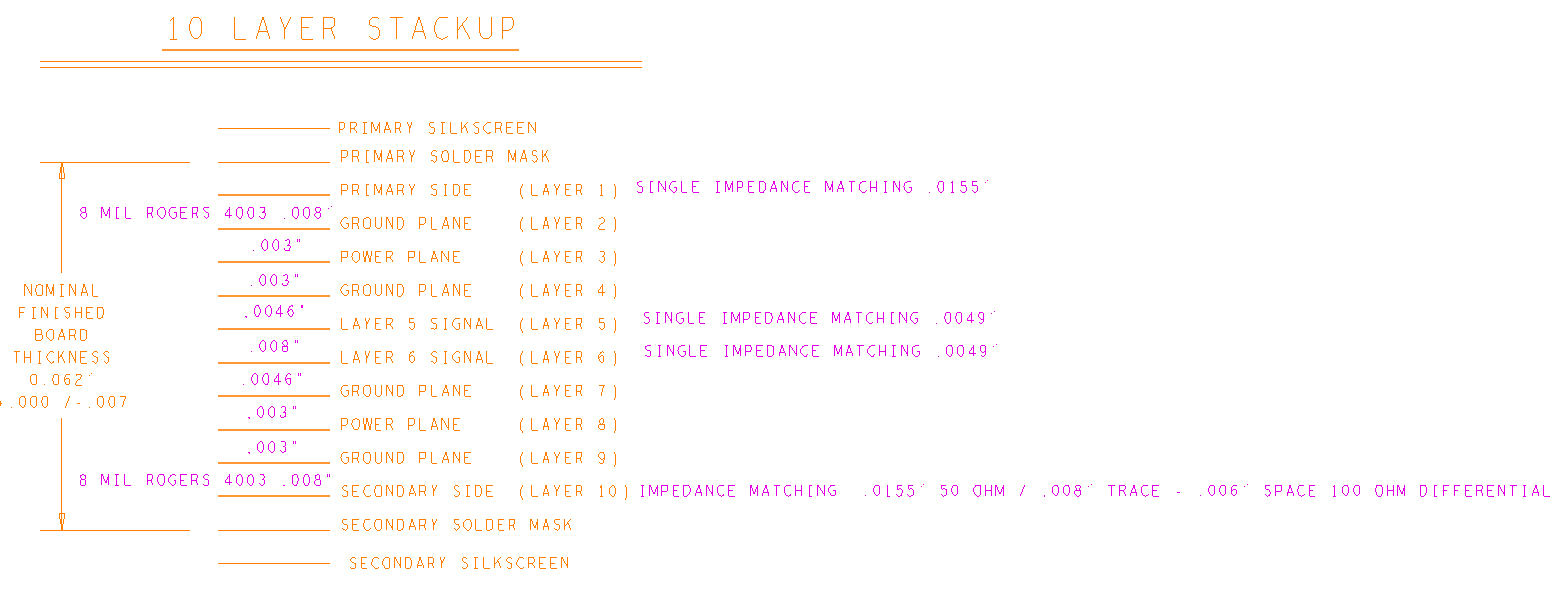
The AD-FMCOMMS3-EBZ is a 10 layer board.
Design Cross Section
Subclass Name |
Type |
Material |
Thickness (MIL) |
Conductivity (mho/cm) |
Dielectric Constant |
Loss Tangent |
Shield |
Width (MIL) |
|---|---|---|---|---|---|---|---|---|
SURFACE |
AIR |
0 |
1 |
0 |
||||
TOP |
CONDUCTOR |
COPPER |
2.025 |
595900 |
1 |
0 |
8.00 |
|
DIELECTRIC |
FR-4 |
8 |
0 |
3.38 |
0.035 |
|||
L2_GND |
PLANE |
COPPER |
1.35 |
595900 |
1 |
0.035 |
Y |
|
DIELECTRIC |
BT_EPOXY |
3 |
0 |
4.10 |
0.02 |
|||
L3_PWR |
PLANE |
COPPER |
1.35 |
595900 |
1 |
0.035 |
Y |
|
DIELECTRIC |
FR-4 |
3 |
0 |
4.10 |
0.035 |
|||
L4_GND |
PLANE |
COPPER |
1.35 |
595900 |
1 |
0.035 |
Y |
|
DIELECTRIC |
BT_EPOXY |
4.60 |
0 |
4.10 |
0.02 |
|||
L5_SIG |
CONDUCTOR |
COPPER |
1.35 |
595900 |
1 |
0.035 |
3.80 |
|
DIELECTRIC |
FR-4 |
8 |
0 |
4.10 |
0.035 |
|||
L6_SIG |
CONDUCTOR |
COPPER |
1.35 |
595900 |
1 |
0.035 |
3.80 |
|
DIELECTRIC |
BT_EPOXY |
4.60 |
0 |
4.10 |
0.02 |
|||
L7_GND |
PLANE |
COPPER |
1.35 |
595900 |
1 |
0.035 |
Y |
|
DIELECTRIC |
FR-4 |
3 |
0 |
4.10 |
0.035 |
|||
L8_PWR |
PLANE |
COPPER |
1.35 |
595900 |
1 |
0.035 |
Y |
|
DIELECTRIC |
BT_EPOXY |
3 |
0 |
4.10 |
0.02 |
|||
L9_GND |
PLANE |
COPPER |
1.35 |
595900 |
1 |
0.035 |
Y |
|
DIELECTRIC |
FR-4 |
8 |
0 |
3.38 |
0.035 |
|||
BOTTOM |
CONDUCTOR |
COPPER |
2.025 |
595900 |
1 |
0 |
8.00 |
|
SURFACE |
AIR |
0 |
1 |
0 |