Intrinsic Safety Design
Introduction
The AD-ETHERNETAPLDEVICE-SL has been certified for Ex ia IIC Ga intrinsic safety requirements according to IEC 60079-11:2011 standard. It also complies with 2-WISE (two-wire intrinsically safe ethernet) standard dictated by IEC TS 60079-47.
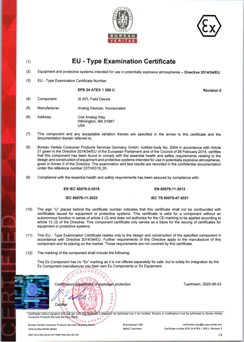
Figure 1 AD-EthernetAPLDevice-SL Intrinsic Safety Certificate
Tip
The full copy of the certificate can be found here:
AD-EthernetAPLDevice-SL Intrinsic Safety Certificate
Key Parameters
The 10BASE-T1L Ethernet connection can only be considered 2-WISE, especially for the APL Field Device if it passed the specification of a Power Load Port indicated in IEC TS 60079-47.
Disclaimer
The electrical circuits must be protected by encapsulation within the final device. Such an encapsulation is required for:
protection against spark ignition (IEC 60079-11:2023, 6.6.2.1)
protection against thermal ignition (IEC 60079-11:2023, 6.6.2.2)
rating of electrical components from which the intrinsic safety depends (IEC 60079-11:2023, 6.6.6)
application of separation distances through casting compound (IEC 60079-11:2023, Table 7, column 3)
The corresponding sections of EN 60079-11:2012 shall be applied in addition.
An enclosure is not part of this certification.
The full technical requirements of manufacturer’s specification must be considered for the final device. The local temperature range of -40°C ≤ Tamb ≤ +85°C shall never be exceeded. The maximum surface temperature does not exceed 135°C (for T4), if the end user fulfills all requirements.
This Ex Component has no “Ex” marking as it is not offered separately for sale, but is solely for integration by the Ex Component manufacturer into their own Ex Components or Ex Equipment.
Circuit Analysis
Other than the classical considerations for intrinsic safety component selection, such power ratings, distances or temperature coefficients, special attention has been paid to the blocks highlighted in the diagram.
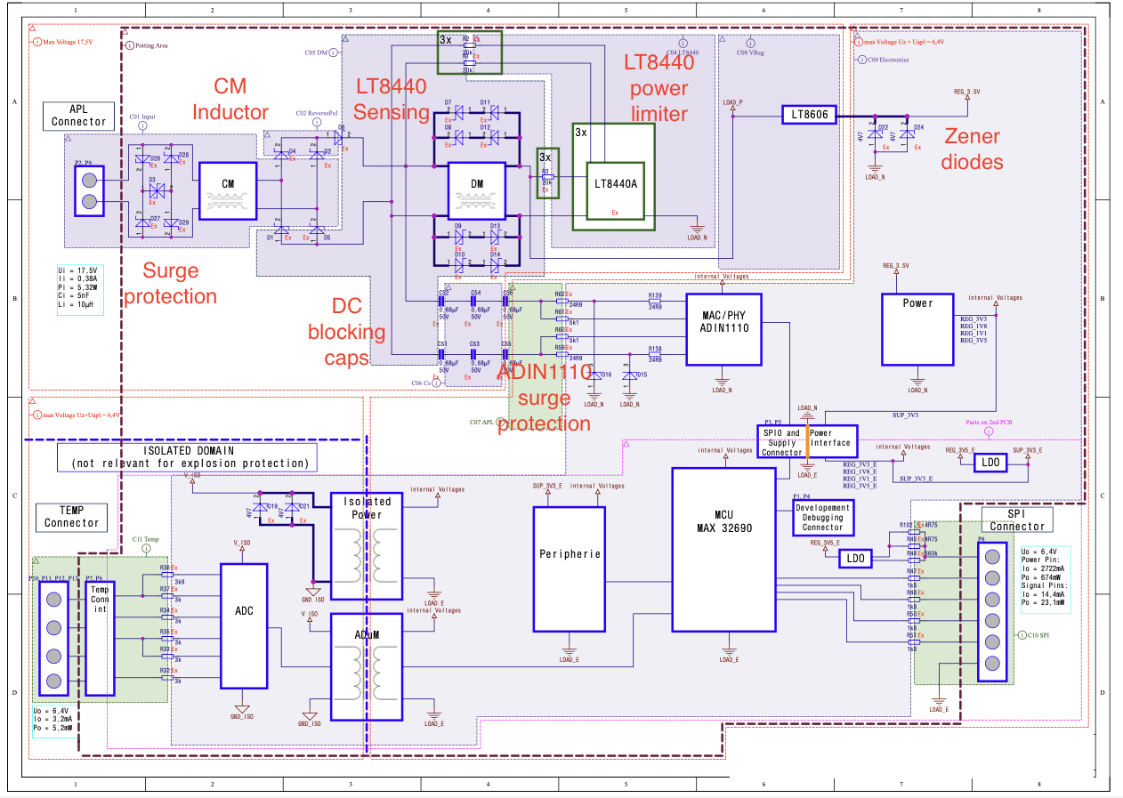
Surge Protection
Ethernet-APL specifications requires the use of 25A surge protection devices to avoid damage due to high voltage transients. While this requirement is not part of the intrinsic safety certification, it is important to use a low capacitance diodes to minimize the TVS diode capacitance to guarantee proper Ethernet communication.
Common-mode Inductor
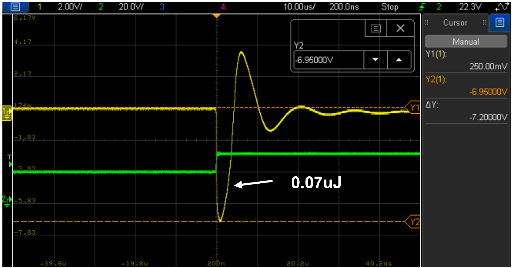
The primary function of this inductor is to remove the common mode noise that can be present in the field wiring. The required value exceeds the maximum value for intrinsic safety.
To qualify the component, independent measurements have been performed to verify that the energy stored by the inductor is within allowable limits at different conditions. Maximum allowable energy is 20uJ for Ex ia IIC Ga equipment or device.
Intrinsic Safety Protection for APL Circuit
The Ethernet and power protection path is responsible for the Field Device to be intrinsically safe, along with other connections or ports outside of the board. It consists of magnetics and diodes at the front end to control common mode and differential impedances, and to control signal polarity and contain stored energy in capacitors and inductors (fault protection). LT8440 works in this path to limit total power dissipation in the module, keeping heat under control in all conditions. While other ports may be implemented using resistors as current limiters, hence it will indirectly limit power and energy. The light-blue highlights on the simplified circuit below indicates the protection parts or “barriers” that prevent excess energy which protect against explosion, more information can be learned on IEC 60079-11.
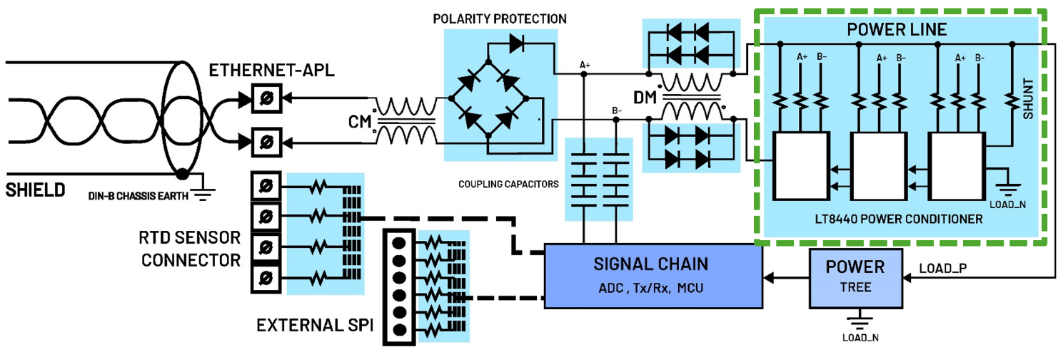
Figure 4 APL Front End Circuit with LT8440 Power Conditioner
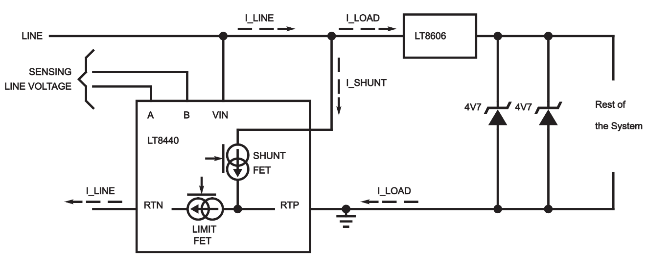
LT8440 as Power Limiter
The LT8440 has been specially designed for Ethernet-APL Intrinsic Safety applications. It serves two primary functions, the first one is to minimize input current glitches that could disrupt Ethernet communication, and the second one is to limit the power that can be delivered to the system in case of a faulty condition. The LT8440 adjust the maximum current allowable to the load by sensing the input voltage provided by the field switch to deliver the maximum possible power to the load. In our design, the sensing input pins from the LT8440 has been connected after the diode bridge as this allows for a higher capacitance values.
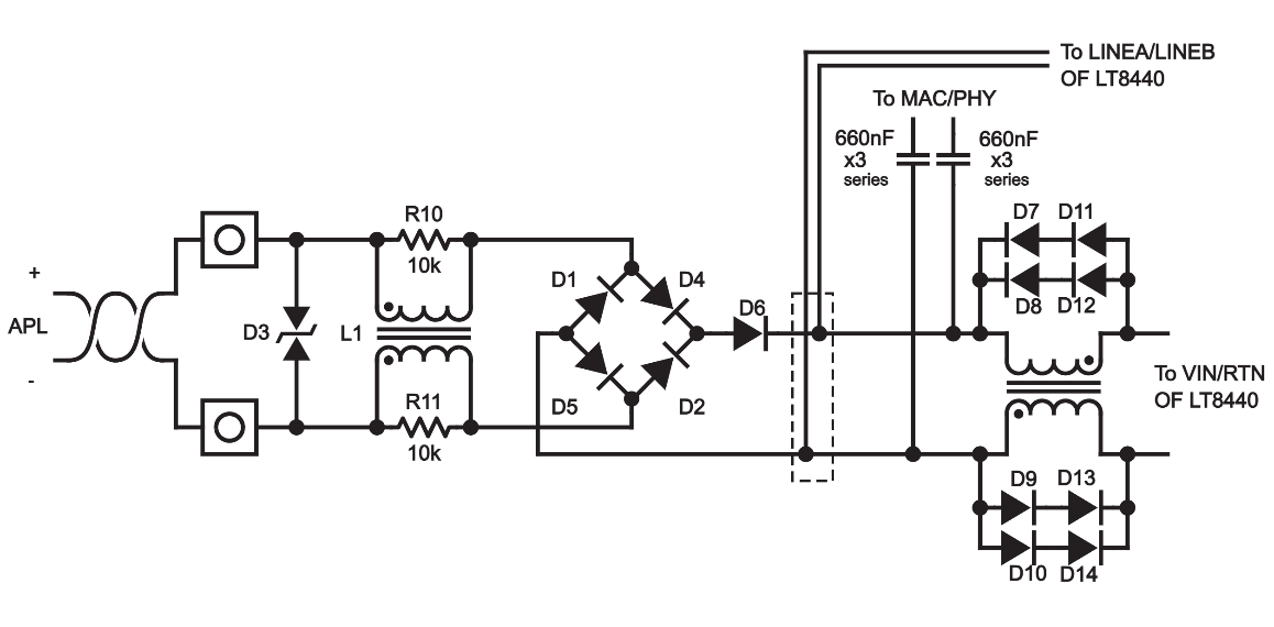
Figure 5 Required Frontend Design with Large Effective Capacitance and Inductance on the Load Side
Zener Diodes
The Zener diodes will limit the maximum voltage seeing by the circuit in case of failure. In the specification of IEC TS 60079-47, the maximum voltage is 17.5V. But in addition to that, for a low-power field device, smaller parts are needed which are commonly have low voltage and power ratings, so the selected Zener must be much lower than 17.5V. In the reference design the typical Zener diode used as protection has a Zener voltage of 5V.
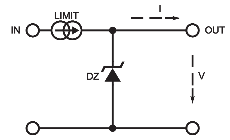
When using the Zener Diode as voltage limiter, it’s placed in combination with a current limiter, this current limiter can be a resistor or a semiconductor-controlled limiter. In the reference design, the Zener diodes are in combination with the LT8440 if there is a failure or faulty condition like the shorting failure of the buck converter in between them for example. The usual combination is done to make sure both voltage and current are limited, resulting in restricting the power, hence restricting energy. When the LT8440 and Zener diodes are combined, it creates a regulated source in which power is controlled, and the voltage amplitude is protected even during fault. Which allows for selection of cheap and very small parts that are low-voltage and low-power in ratings, while not violating intrinsic safety.
General Purpose Diodes
Diodes serve several functions. For the purposes of intrinsic safety, diodes can fail to open circuit or short circuit.
1. The ethernet cable can be connected in either polarity, so either of the connector pins may be positive. The APL requires polarity insensitivity at the connector. The diode bridge provides this polarity insensitivity, and the additional series diode provides redundancy for failure protection. These diodes must be Schottky type to have the lowest forward voltage drop. Voltage drop in this path dissipates power, making less available to the load.
2. All capacitances in the circuit can store energy, and only Schottky diodes are considered fast enough to catch that energy before it can propagate out to the connector and cause a spark in the case of a short circuit. For ‘Ex ia’ level protection, we need 3 polarity protection diodes in series to account for 2 simultaneous short circuit failures. The diode bridge and the additional series Schottky diode provide this protection.
3. The differential mode (DM) inductor can store energy that must be dissipated safely in the event of an open-circuit fault. The bank of diodes connected in parallel to the DM choke only operates in the event of an open circuit in the inductor that would otherwise create a voltage spike. These diodes must be redundant in parallel to reach ‘Ex ia’ protection. Three diodes in series are recommended for higher or wider operating temperature range because of the diode forward voltages being dependent on ambient temperature, which the diodes must block the ethernet signal of 1Vp-p during forward biased, and must not be distorted by diodes conducting across the inductor. But if size and component count are a critical factor, it can be reduced to 2 diodes in series in lesser or narrower temperature range.
Capacitor as DC Blocker
Because of the nature of capacitors during steady state or DC analysis, the capacitors simply block direct current, in which it is suitable protection by acting as a blocker for DC Power and DC Energy. In the APL field device circuit, the capacitors responsible for blocking the DC, while allowing the AC signal to pass through for the Ethernet Data is designed then to be rated during fault-short by simply being a DC blocker.
Resistors
Resistors are often used to limit current if a protected component experiences a short circuit failure. ICs such as the LT8440 are considered to fail to a pin-to-pin short circuit, so it must be protected. As defined in the IEC 60079-11, infallible resistors (those of film type and suitably large to allow infallible space between ends) can only fail to an open circuit state. The main reason to use redundant resistors is to dissipate heat in the event of a short circuit elsewhere in the system. If a single resistor is physically large enough with better power dissipation, then a single resistor is sufficient.
Explosion Protection Levels and Redundancy Approach
In a circuit analysis when safety against explosion is involved, assume or anticipate the fault that will occur in the circuit, and the protection parts of the circuit must withstand permissible or maximum electrical parameters that can happen during circuit failure dictated by the requirements or specifications.
The design of the Intrinsic Safety protection is categorized by the level of protection indicated by IEC 60079-11. The more stringent the protection, the stricter the circuit implementation will be, this involves the de-rating or safety factor of component ratings and the redundancy of protection parts based on the number of countable faults.
Category |
Safety Factor |
Countable Fault |
Ex ic |
x1.0 |
0 |
Ex ib |
x1.5 |
1 |
Ex ia |
x1.5 |
2 |
Countable faults are the type of faults or failure that if it happens, it will caused explosion, hence it is “counted” because they are critical and must be prevented by doing duplication or redundancy.
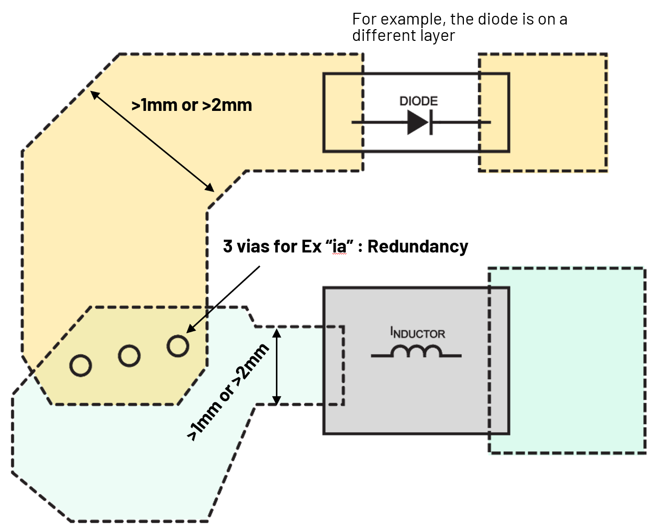
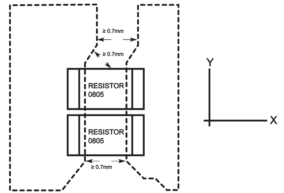
PCB Layout Considerations
IEC 60079-11 requires PCB clearance and creepage requirements, depending on the protection level and encapsulation involved, clearance from different insulated layers, or if the traces are exposed in air. A simplified table is shown below, although the complete distances table for different input conditions are provided in IEC 60079-11.
This states that there should be a distance for the traces for different permissible voltages, and when in between the protection parts. These distance requirements are not just for the traces in the same layer, but also on the different layers, meaning the clearance requirement is 3-dimensional.
Depending on the Level of Protection, there will be required copper thickness and redundancy of vias that may involve.