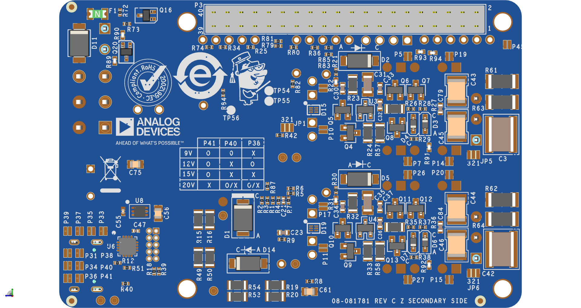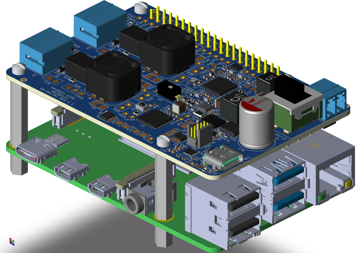
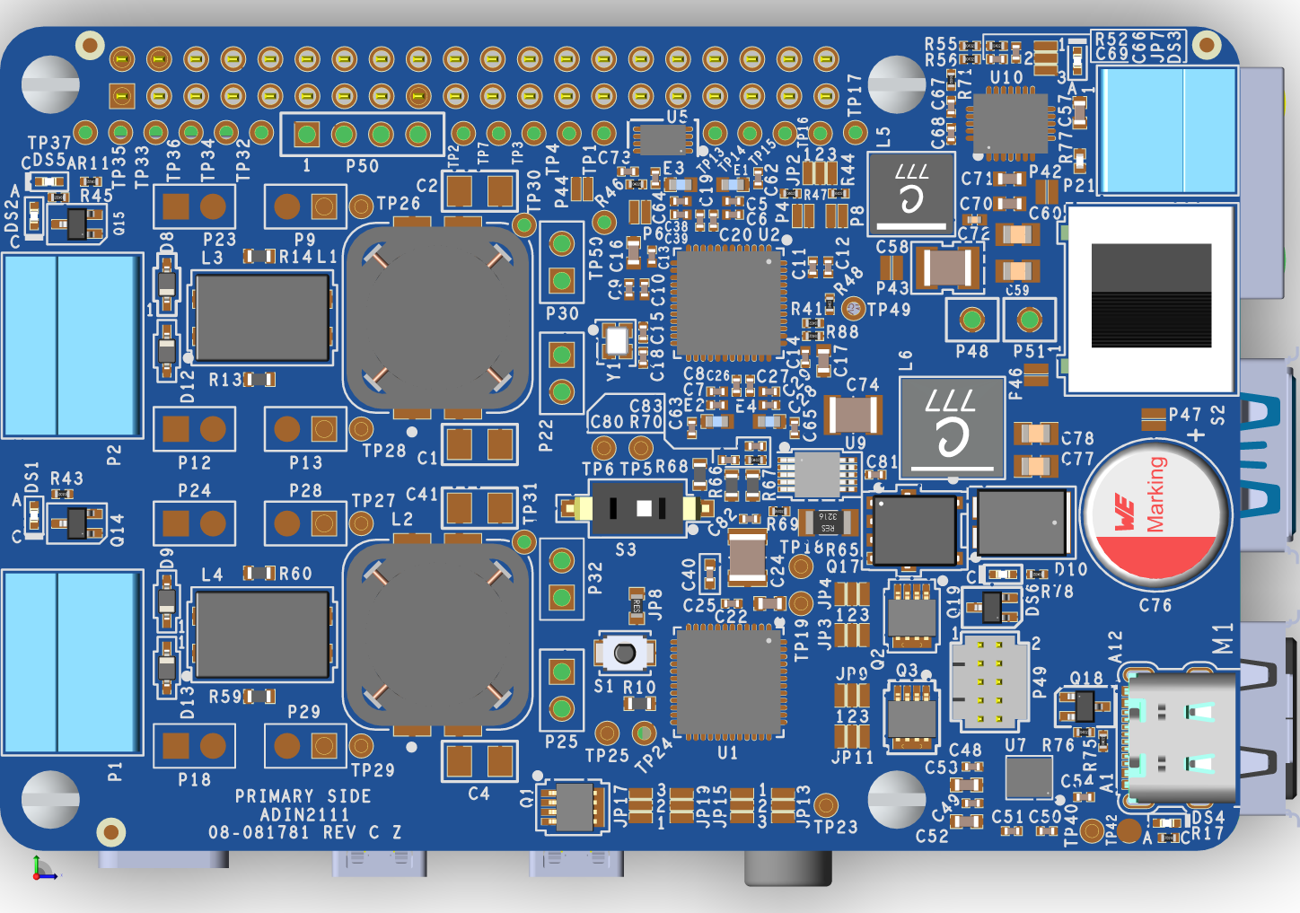
Primary Side
10BASE-T1L Ports (P1 and P2)
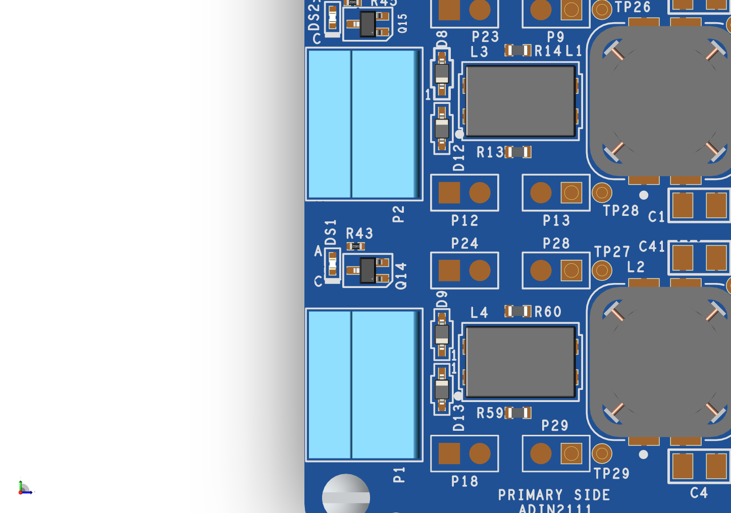
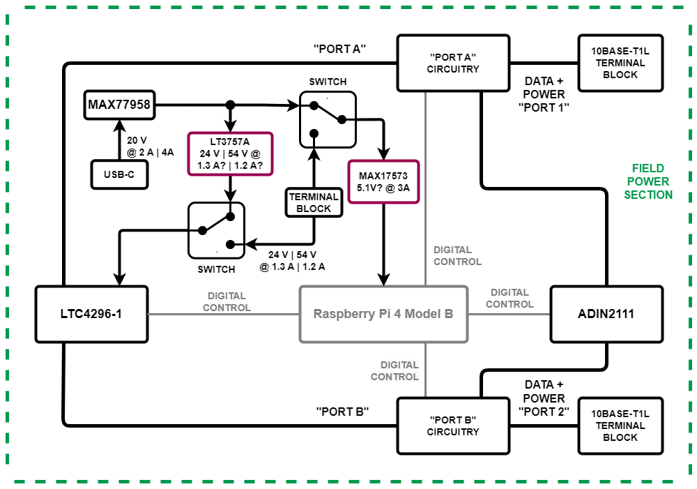
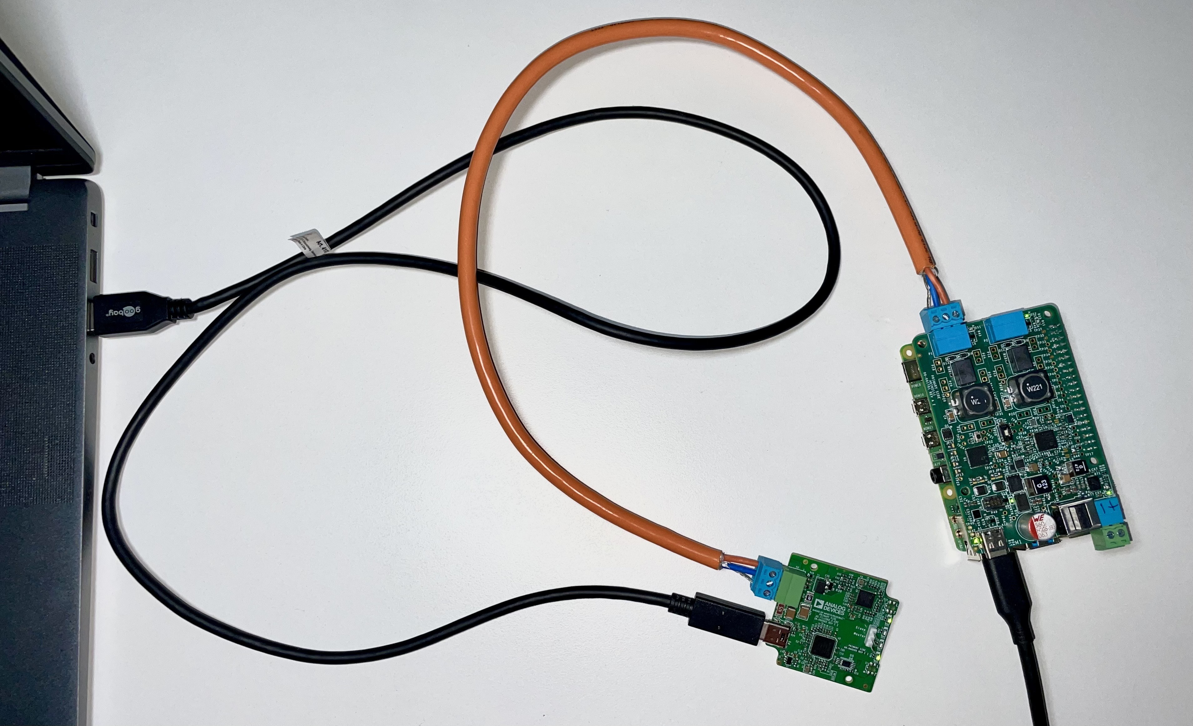
The AD-RPI-T1LPSE-SL evaluation board features two 10BASE-T1L ports, allowing connection to up to two PDs. Each port supports independent control of power sourcing and data transmission.
P1 and P2 are 3-pin terminal blocks designed for twisted pair cables, with optional shielding. These ports deliver class-dependent DC voltage to connected PDs and transmit AC-coupled data signals for 10BASE-T1L communication. Both ports include protection against overvoltage and electrostatic discharge (ESD) events.
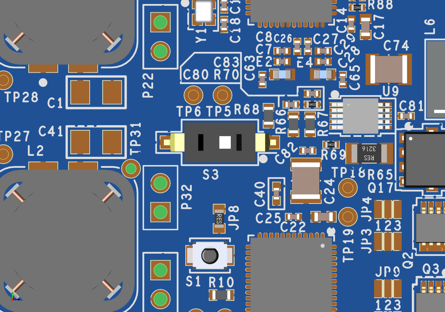
When the board is powered via USB-C, the default output voltage is 24V, generated by the LT3757A flyback boost converter, suitable for SPoE Classes 10–12. To enable SPoE Classes 13–14, which require 54V, switch S3 to activate the higher voltage output.
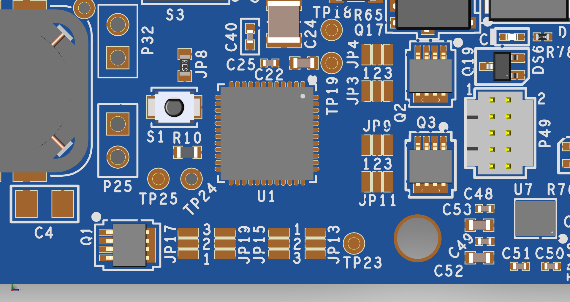
The USB-C uses the MAX77958 standalone USB Power Delivery (PD) controller, which can be programmed using the P49 header. When power is supplied via the terminal block P21, the voltage can be set to 24V or 55V using the customers power supply. The supply port can be selected via the S2 switch.
In either of the cases, to power the Raspberry Pi, 5V is generated using the MAX17573.
ADIN2111
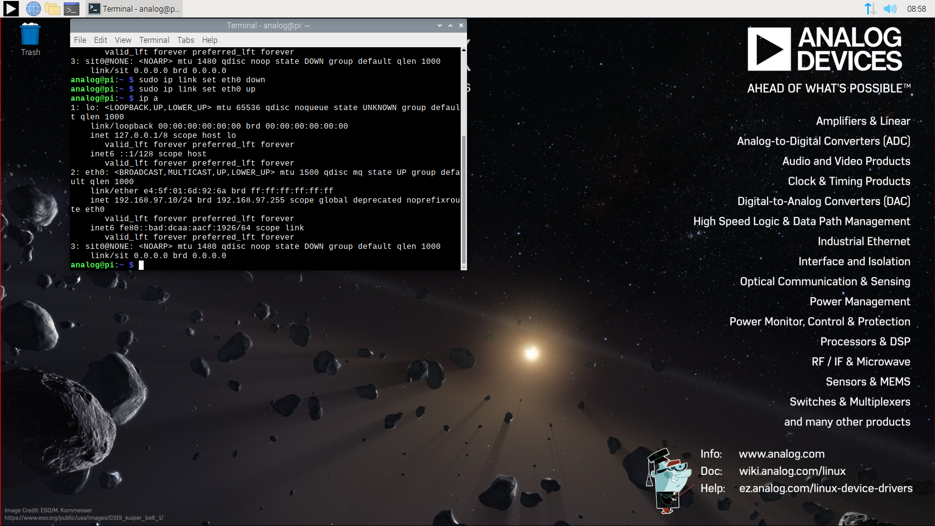
The onboard ADIN2111 PHY provides the 10BASE-T1L connection to the host platform board. The ADIN2111 is connected to the Raspberry Pi using the SPI0 port of the Raspberry Pi.
The ADIN2111 features selectable peak-to-peak transmit voltage levels of either 1.1V or 2.4V. These levels can be configured by adjusting the P6 and P4 solder jumpers for PHY1 and PHY2, respectively:
Disconnected: 2.4V
Shorted: 1.1V
The generic SPI protocol is half duplex. Therefore, it is not possible to write frame data into the MAC_TX register and read from the MAC_RX register at the same time. To achieve full duplex transmission on Ethernet at 10 Mbps, OPEN Alliance SPI must be used. To select which SPI protocol to use, the JP1 (located on the bottom of the board) solder jumper should be configured as follows:
JP3 Position |
SPI Mode |
Across 1 and 2 |
AD (Generic SPI) |
Across 2 and 3 |
OA (OPEN Alliance SPI) |
The ADIN2111 supports software power-down functionality for each port independently after power-up or reset. To enable this feature:
For PHY1, short the P8 jumper.
For PHY2, configure the JP2 solder jumper as follows:
JP4 Position |
Software Power-down |
Across 1 and 2 |
Disabled |
Across 2 and 3 |
Enabled |
LTC4296
The LTC4296 is a five port, single-pair power over Ethernet (SPoE), power sourcing equipment (PSE) controller. The LTC4296-1 is designed for interoperability with powered devices (PDs) in 24 V or 54 V systems. PD classification via the serial communication classification protocol (SCCP) and maintain full voltage signature (MFVS) ensure full operating voltage is only applied to the cable when a PD is present. PD initiated sleep and wake-up are supported. Telemetry, status, and software control features are accessed via SPI bus interface with packet error code (PEC) protection.
The LTC4296 is directly powered from the LT3757A flyback boost converter or from the 24V or 55V power supply connected to the P21 terminal block.
The device by default is configured to operate in SPoE Class 12 (24V nominal) or SPoE Class 14 (54V nominal) mode. In order to use classes 11 and 13, the following solder jumper configurations are required:
The LTC4296 also supports SPoE Class 10. To enable this functionality, specific resistor changes are required:
High-side circuit breaker resistors:
For PORT1, replace R15 or R16 with 1.6Ω, 1/10W resistors.
For PORT2, replace R49 or R50 with 1.6Ω, 1/10W resistors.
Low-side sensing resistors:
For PORT1, replace R19 or R20 with 0.4Ω, 1/10W resistors.
For PORT2, replace R53 or R54 with 0.4Ω, 1/10W resistors.
The complete power requirements for the SPoE classes are shown in the table below: