Power Description
Ethernet-APL Field Platform Power Description
Introduction
The AD-ETHERNETAPLDEVICE-SL follows specification based on Ethernet-APL Port Profile Power consumption. As a complete system, with the power conditioner involve as main part of the entire power tree (along with switching converters and LDO regulators), the following signal names are identified:
As shown in Table 2 - Electrical Characteristics of Power Classes, the AD-ETHERNETAPLDEVICE-SL has a required Power Class A specification. For the complete table, read the document’s Table 6 of Ethernet-APL Port Profile specification.
Circuit Analysis
The main goal for the power circuit of the reference design is to make sure that even if the power produced from the source port is as minimal as 540mW, or if the power received of the load port (field device or the AD-ETHERNETAPLDEVICE-SL itself) is as minimal as only 500mW for Power Class A, the board should still operate normally on those circumstances. Which means the reference design board should consume low power as possible that it doesn’t violate the boundaries of line current and voltage range indicated in the specifications.
This is why the LT8440 Power conditioner is important and acts as main anchor part of the design, because it pulls at minimum 20mA to drive the protection diodes of the APL line to conduct power and provide data communication, and also enters shunt regulation mode to pull enough power for the device to function, while also limiting the current and power at 650mW maximum worst case to prevent overheating to comply with intrinsic safety. Ideally its best to select power parts of the best efficiency so it will only pull much lesser current on the LINE_P and LOAD_P during normal operation. However, if cost and small form-factor is the primary concern (in this case on this reference design with DIN-B form factor), we can slightly compromise the efficiency but making sure first that it won’t violate the line current ceiling it can pull to the LT8440.
Figure 1 Source to Load Simplified 2-WISE/APL Port Connection
LT8440 Operation
The LT8440 can operate on two different constant current regulation: Shunt Regulation Mode and Current Limit Mode, depending on the voltage sensed by the LINEA and LINEB pins of LT8440, and the current that will flow to the LOAD_P thru the system of AD-EthernetAPLDevice-SL, it will dictate the regulation amplitude of the line current and which mode it will regulate. For the complete specification of LT8440, see the Electrical Characteristics on LT8440 datasheet.
The line current will also depend on both the shunt current (I_SHUNT) and LOAD_P current (I_LOADP) as the line current (ILINEP) is the summation of I_LOADP and I_SHUNT shown in Equation 1.
I_LINEP = I_LOADP + I_SHUNTP (1)
During Shunt Regulation Mode, the shunt pin of the LT8440 is conducting in which it satisfies Equation 1.
The shunt pin will conduct if the current I_LOADP is not conducting (0mA) or I_LOADP is only minimal or lesser than the typical Shunt Regulation Mode current indicated in Table 4 so the shunt pin detects the lack of I_LOADP, then the shunt pin pulls more current so that I_LINEP will regulate the current within the boundaries indicated on Table 4.
Shunt current will only be equal to the line current if LOAD_P is operating at No-Load (0mA). If there is a minimal I_LOADP current, the Shunt current self-adjust to be what is indicated on Equation 2, which is simply a linear algebra manipulation of Equation 1.
ISHUNT = ILINEP - ILOADP (2)
For example: for LINE_P voltage of 10.5V, and I_LOADP = 10mA, the Shunt pin will pull the current ISHUNT = 30mA approximately, so that it will satisfy the ILINEP = 40.5mA (for Level 1) or ILINEP = 39.7mA (for Level 2).
The LINEA and LINEB pins sensed the voltage on the input line and dictate the current regulation, the position in which the LINEA/B connected will have a different measured or sensed voltage while still complies to the specifications indicated on Table 3 and Table 4, which is provided completely on the LT8440 datasheet.
The LINEA/B should be connected after the polarity protection diodes indicated in Figure 3, so that the effective capacitances and inductances that will generate discharges of the system is being isolated by the diodes, and it will not be counted to the effective capacitance nad inductance of the input line or the load port, this is based on Table 1 of IEC60079-47, the allowable internal line capacitance is only 5nF, and allowable line inductance is 10uH. This will however result for the sensed voltage to be lower at normal operation because of the forward voltages of diodes reducing the sensed voltage.
At lower sensed voltage, the current regulation of the LT8440 will have a higher offset current, but it is still in line with the electrical specification of LT8440, and the power limiter will still work as intended.
Figure 3 is the designed configuration for AD-EthernetAPLDevice-SL to pass the Intrinsic safety design certification.
Figure 3 Required Frontend Design with Large Effective Capacitance & Inductance on the Load Side
Power Tree Design
Initial step is to design the power parts after the LT8440 with the theoretical assumption of the power at maximum load condition that guarantees to operate the critical signal chain parts of AD-EthernetAPLDevice-SL, which are going to pull power from the LT8440’s LOAD_P node. The performance of the design for current and power on LOAD_P shall not exceed the specifications or shall not trip the limits of LT8440 itself and the APL Specifications.
Tabulating the estimated power budget of AD-EthernetAPLDevice-SL at maximum load based on the datasheets of the significant parts of the signal chain, we can calculate the theoretical power consumption at worst case and select appropriate power parts for the power tree using the LTPOWERPLANNER for the Power Tree calculation.
In the power tree provided in Figure 8 based on estimated power budget at full load.
The reference design incorporates a for the different needed rails, mainly the triple output of 3.3V (3V3), 1.8V (1V8) and 1.1V (1V1) lines to power-up the common parts, a separate 3.3V line (SUP_3V3) dedicated to supplying power for the supervisory circuit, and an isolated 3.3V (ISO_3V3) for supplying the data isolator and A/D Converter temperature sensor interface.
The LT8606 acts as the pre-regulator of the power tree, it has a wide range of input voltage, capable of up to 42V maximum operation, small, efficient, and requires low component, this is suitable to the wide voltage range of 9V to 15V (or 17.5V maximum) on the LINE_P that will translate to a slightly reduced wide voltage on the LOAD_P node, take note that the voltage rating of the selected buck converter is considered with the 2/3 derating. The 350mA max current can provide more leeway (from 2/3 de-rating) and still is suitable for this 500mW system. The UVLO prevents the converter from operating if the LOAD_P voltage from the ethernet cable is too low, thus preventing some faulty operating conditions. Zener diodes are added to clamp the output rail and guarantee it will not exceed the VZ = 4.7V under any conditions, important as overvoltage protection for intrinsic safety, because it relaxes the requirements for picking parts when the voltage and power are much lower after the LT8440 and the Zener diodes.
For simulation using LTSPICE for example (or estimation via datasheet), the LT8606 buck has an estimated efficiency of 90.3% and in the LTPOWERPLANNER power tree, the calculated maximum pulled current is 42.8mA in the input of LT8606, which is also the LOAD_P node. Among the parts for the main voltages 3V3, 1V8 and 1V1, the 1V8 is the one that needs the most current as most of the signal chain parts, which are ADIN1110 and MAX32690, needed the supply voltage of 1.8V. To sustain a better efficiency so it won’t pull too much current from the output of LT8606, we need another buck converter. The selected part for 1V8 output is MAX17626, it is small, high efficiency capable and requires low component count so it’s easy to implement. By simulation using for example the EE-SIM Oasis software (or estimation via datasheet), the estimated efficiency given by the input and output voltages is 83.2% in which is indicated in the power tree of LTPOWERPLANNER.
The 3V3 and 1V1 pulls very low current, so LDO regulators are better and cheaper with negligible effect on power loss. In this case we picked the ADP151 series of LDOs with fixed values for 1.1V and 3.3V because of small form factor, reduced cost and lower component count.
The MAX253 push-pull converter is the selected isolated power part because of minimal design requirement or low component count. Based on the datasheet using 1:1.3 transformer, the estimated efficiency is 84%. This is negligible for estimated drawn current of 4.5mA at the output with calculated output voltage of 4V to 4.3V. The push-pull won’t regulate properly at light load or lower current, so a post regulator LDO is included to provide the fixed 3.3V isolated voltage for the A/D converter and digital isolator. The AVDD of ADFS7124-4 can be sensitive or in risk of noise, so an optional RLC low pass filter is included. Zener Diodes are also included in the MAX253 output to prevent overvoltage by clamping it to VZ = 4.7V during potential overvoltage fault and for general intrinsic safety.
For functional safety specifically on the supply for the supervisory circuit like the MAX42500, the voltage line that is supplying should not be the voltage it monitors. A separate 3.3V line is powering the supervisor using ADP151-3.3V LDO which is labeled SUP_3V3, therefore the MAX42500 will still work properly even if there is an OV/UV event occurring to 3V3, 1V1, and 1V8.
For the external SPI of AD-EthernetAPLDevice-SL, we included a dedicated supply pin of external 3.3V, although it is not counted in the overall power calculation because the SPI’s load specification is not defined. However, the extra power that is available or unused will be dedicated to the external SPI, with the main LDO selected is ADP123. The LDO’s dedicated VOUT feedback is usable for application were we need to modify the output voltage it will regulate. This is specific for intrinsic safety case where a limiting resistor is added, but the output should still maintain in 3.3V.
Based on the calculation of the LTPOWERPLANNER, the maximum power or full load is approximately 300mW which is the estimated power pulled on the LOAD_P, and the I_LOADP only pulls an estimated maximum current of 42.85mA, which didn’t exceed the limit of 55.56mA of APL.
Note: The actual power on the board can be much lesser than the calculated power because the parts like the MAX32690 and ADIN1110 won’t require to fully utilized that much power to function. The actual or measured power and current are discussed on the Power Consumption section.
Power Consumption
Characterizing the performance of the LT8440 Power Conditioner and the entire Power Tree, the following curves are captured at ambient temperature of 25 degrees Celsius (typical).
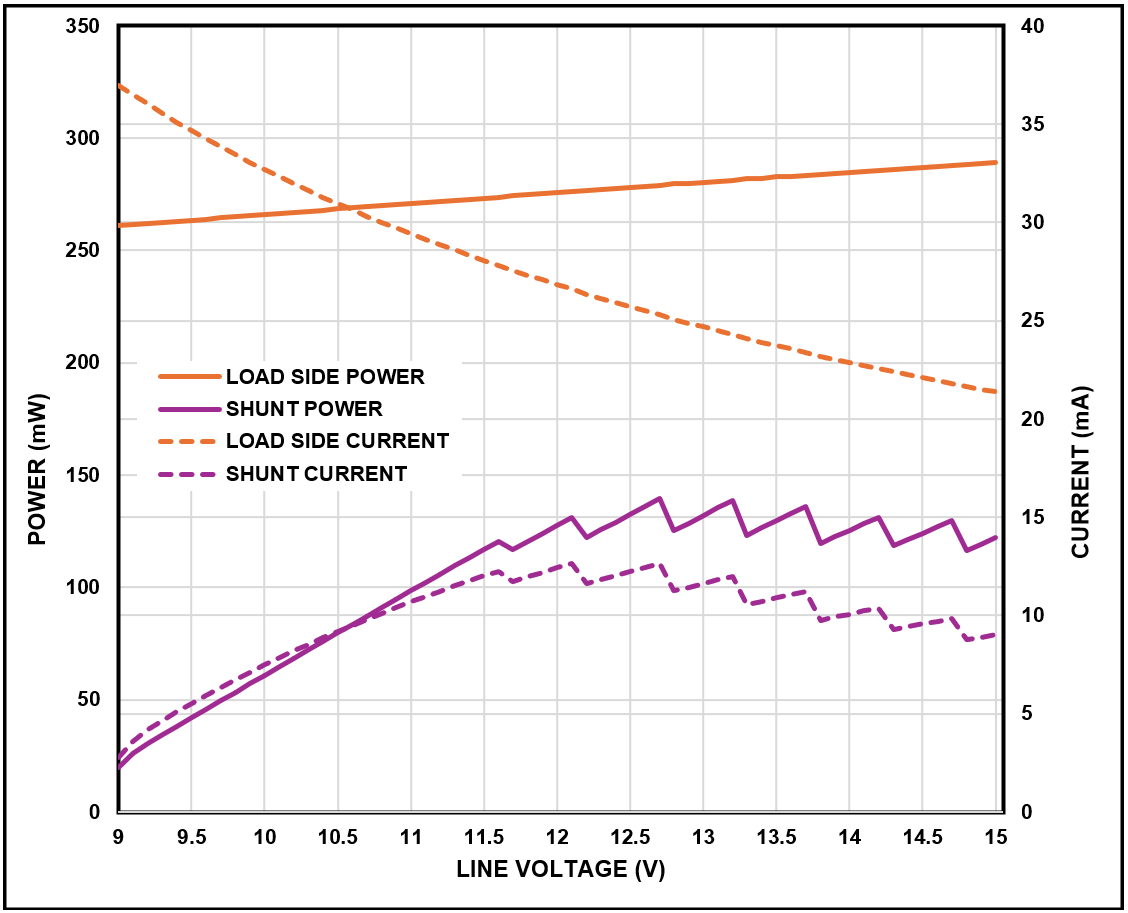
The load side power and current are pulling approximately 288mW and 21.38mA respectively at 15V line voltage, these are the highest parameters that the load side or LOAD_P node will consume during normal operation.
For 9V line, the load side power and current are pulling approximately 260.9mW and 19.706mA respectively at normal operation.
The reference design is operating on LT8440’s shunt regulation mode, where the shunt pin is pulling current. The shunt power and current are pulling approximately 122.03mW and 9.03mA respectively at 15V line voltage, while its approximately 19.71mW and 2.79mA respectively at 9V line voltage. The highest shunt power occurred at 12.7V line voltage which is approximately 139.46mW.
The shunt and load side power are small enough to not violate the APL limit when adding the two parameters.
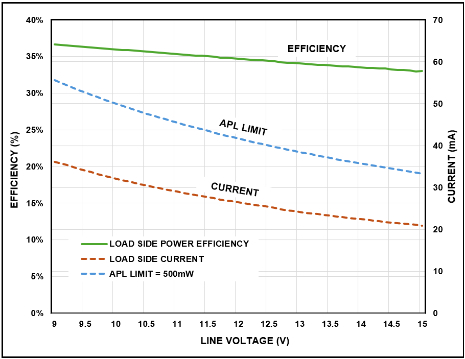
The power tree was designed with the intention of prioritizing the small form factor and cost of parts, so there is a trade-off in the power efficiency for these power parts that are connected after the load side of LT8440.
As shown in Figure 6, the efficiency in range of 33.04% up to 36.65% which is not high and is a significant trade-off despite the very low power consumption, as long as it does not exceed the APL Limit power consumption of 500mW. Which on another point of focus, the efficiency can be trade-off, but the power pulled, or to be more specific, the current being pulled should be low enough that it would not exceed the current ceiling of the APL limit as shown also in Figure 6. So, when sacrificing the efficiency, it will pull more current and power, but those two parameters must not exceed what is indicated on the APL requirements like the 55.56mA maximum current at 9V, and the 500mW limit for the entire line voltage range.
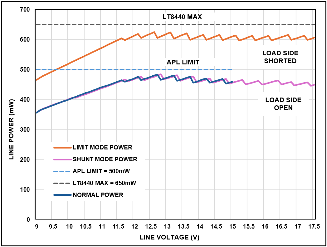
Figure 7 LINE_P Power Performance at Normal Operation, Shorted and Opened Load
Speaking of the line voltage range of APL, the actual entire power consumption range of the whole reference design is measured, the power curves are shown in Figure 7. During normal operation, which is for the boundaries of APL profile specs in the line voltage range of 9V to 15V, the maximum power occurred at LINE_P for line voltage of 12.7V is 484mW, which if compared to the open or disconnected load side of LT8440 at shunt mode, the power is the same 484mW at 12.8V line voltage instead.
For Intrinsic safety scenario at line voltage range of 9V to 17.5V as dictated by IEC60079-47 standard, the maximum APL line power is 625.62mW during the scenario that the load side is intentional faulted/shorted, it did not exceed the maximum die power rating of 650mW, and is within below the 5.32W specification of IEC60079-47, therefore the LT8440 is doing its function as a power conditioner at normal operation and as a power limiter during fault scenario.
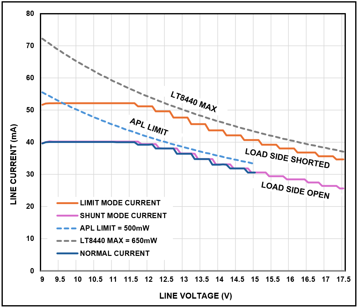
Figure 8 LINE_P Current Performance at Normal Operation, Shorted and Opened Load
The triangular nature of the power curve of LINE_P is a result of the staircase like nature of the I_LINEP or APL line current. This is from the inherent design or construction of the LT8440 silicon in which it has hysteresis in its sensing of voltage during current regulation, so the shifting of current regulated has hysteresis transition first whenever the sensed voltage changes or varies.
For the line currents, none of it exceeds to the limits of APL during normal operation, and also shorted operation of IEC60079-47 as shown in Figure 8.
For questions and more information, please visit the EngineerZone community or contact your local ADI representative.