EVAL-AD-IMP2501-SL
OVERVIEW
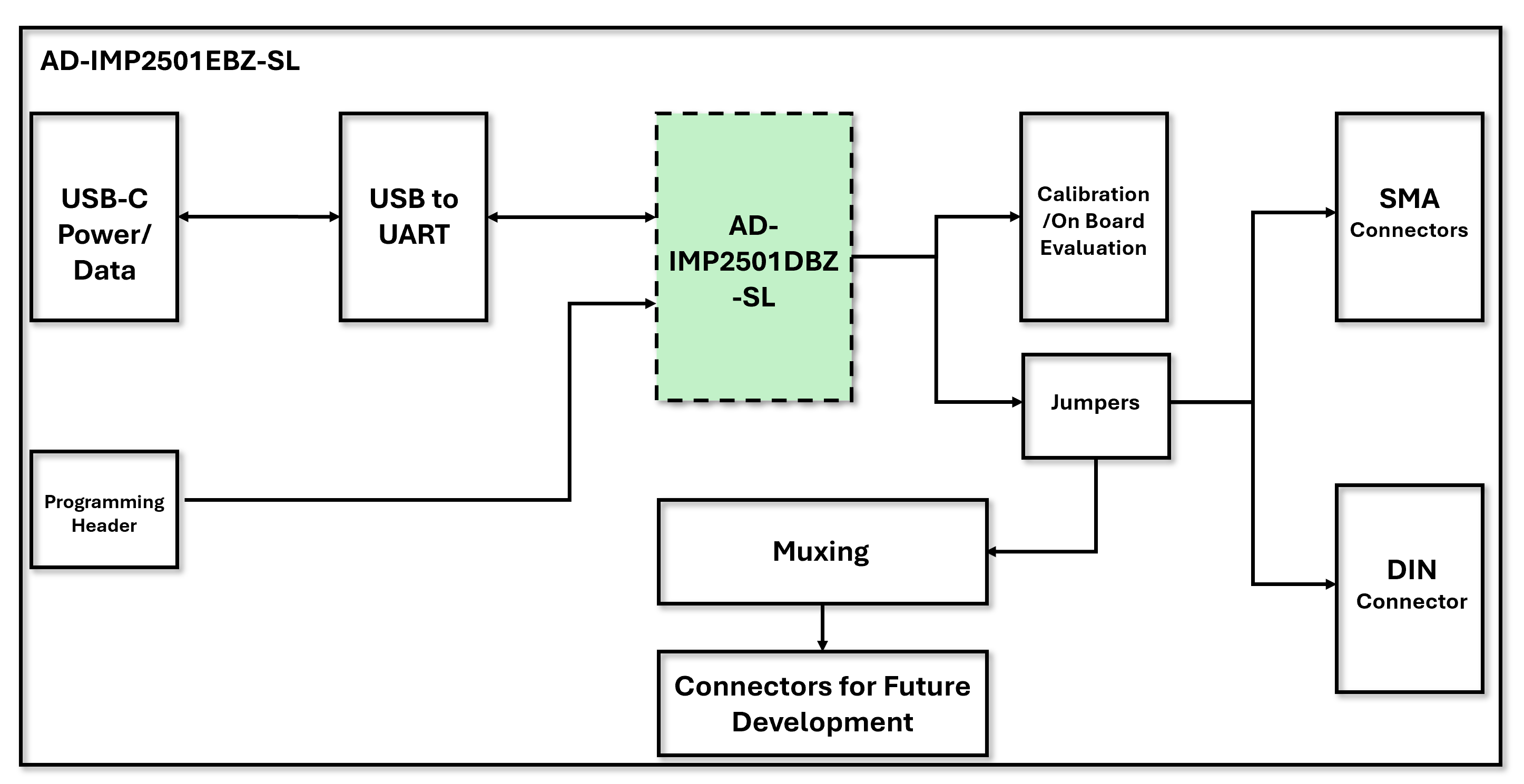
The EVAL-AD-IMP2501-SL is an impedance analyzer demonstrator and technology evaluation system comprised of both the AD-IMP2501DBZ-SL and the AD-IMP2501EBZ-SL boards. The AD-IMP2501EBZ-SL is the carrier board that allows for simplified host PC communication interfacing, varying electrical load connections, and easier setup/debug. The AD-IMP2501DBZ-SL is the electrical impedance spectroscopy module, capable of tetrapolar impedance measurements up to 250 impedance samples per second. It integrates AC waveform signal generation from 0V - 2.4V at 1Hz up to 1.5MHz, differential voltage measurement, current return measurement, and full impedance processing with an arm cortex M4 microprocessor. All in a 400mm square PCB.
Features
The AD-IMP2501DBZ-SL is a high-performance, impedance analyzer module.
Highly compact, 31.24mm x 12.83mm System-on-Module (SOM)
Impedance measurements from 0.1 Hz to 1.5 MHz
Current or Voltage drive application modes
16-bit acquisition channels
Operates from a single 5V supply
UART interface (additional BLE 5.2, USB, and SPI hardware support capable)
Meets patient leakage requirements for IEC 60601-1*
6 display mode formats in SI units
Command line, Graphical user interface, and Python API for easy system evaluation and data collection
*Current hardware implementation is dependent on voltage drive levels. The hardware can be modified to limit the current depending on application specifications and voltage drive needs
The AD-IMP2501EBZ-SL is an easy to use evaluation and development board that enables convenient access to the functionality of the AD-IMP2501DBZ-SL Impedance Analyzer Measurement Module.
USB C connector provides power and serial communication to host PC
On board FTDI USB to UART conversion
DIN and SMA connectors and for interfacing with an external load
On board loads with jumper configurations for testing and evaluation without external components or connections
Applications
Surgical Tools
Surgical Tissue Sensing
Medical Diagnostics and Life Sciences Devices
Bio-Z and Vital Signs Applications
Electronics Testing Systems
Chemistry Systems
Laboratory Bench-top Sensing Applications
Research in Industry or Academia
System Architecture
Specifications
TBD from the characterization table what we want to include here:
Parameter |
Min |
Typical |
Max |
Units |
|---|---|---|---|---|
Vin |
4.6 |
5 |
20 |
V |
Load Range |
V |
|||
Relative Accuracy |
0.2 |
0.05 |
% |
|
Iout |
mA |
|||
Vout |
0.1 |
2.4 |
V |
|
Samples/s |
||||
Frequency Range |
0.1 |
1500000 |
Hz |
|
DC Offset |
0 |
V |
…
AD-IMP2501EBZ-SL Package Contents
AD-IMP2501EBZ-SL Impedance Demonstration Board
USB Cable
AD-IMP2501DBZ-SL Package Contents
AD-IMP2501DBZ-SL Impedance Analyzer Measurement Module
Important
It is critical to purchase both the the AD-IMP2501DBZ-SL Impedance Analyzer Measurement Module and the AD-IMP2501EBZ-SL Impedance Demonstration Board. These are sold separately.
Quick Start
Follow these steps to start evaluating the AD-IMP2501DBZ-SL:
Driver Installation
Terminal Emulator/GUI Installation
Hardware Setup
Command Line or GUI Operation
Performing Impedance Measurements
These steps are explained in detail in the following sections.
Hardware User Guide
The AD-IMP2501DBZ-SL and AD-IMP2501EBZ-SL are designed for evaluating impedance analysis technology in an application that requires a small form factor and wide frequency range. This platform is designed to get an impedance analysis evaluation set-up running quickly with only a provided USB cable and a computer. This hardware guide will walk the user through the basic setup, the varying jumper configurations for different measurement modes, and how to interface with an external load that is more specific to his or her application.
Equipment Needed
Required Equipment
AD-IMP2501DBZ-SL
AD-IMP2501EBZ-SL
USB C Cable
PC
USB drivers and terminal emulator required. Please see Software User Guide for instructions to download and install on your PC if not already installed.
Optional Equipment
Programming equipment for Firmware Updates
MAX32625PICO2 with ribbon cable
Impedance measurement accessories. Available from various test and measurement manufacturers, for example:
Calibration Standards and Accessories
LCR Meter for verification
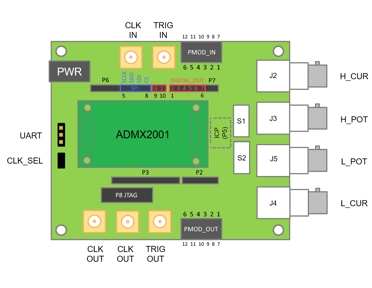
EVAL-ADMX2001EBZ Terminal Description
Terminal Name |
Description |
|---|---|
H_CUR |
Signal source terminal. It generates the excitation required for measurement. This terminal can source up to +/-5V @ 50mA |
H_POT |
Voltage sense terminal. Connect to H_CUR at the device under test (DUT) |
L_POT |
Voltage sense terminal. Connect to L_CUR at the device under test (DUT) |
L_CUR |
Current sense terminal. Return path for the excitation signal. Connect to the opposite end of the DUT as H_CUR |
UART TX |
UART transmitter pin. Connect to TX pin on the UART to USB cable. Uses 3.3V logic |
UART RX |
UART receiver pin. Connect to RX pin on the UART to USB cable. Uses 3.3V logic |
UART GND |
UART ground. Connect to ground pin on the UART to USB cable |
CLK_SEL |
Jumper selection of internal or external clock. Set to internal for default operation |
TRIG_IN |
Trigger input. Use for hardware-timed acquisition only, otherwise leave disconnected |
TRIG_OUT |
Measurement complete trigger out |
CLK_IN |
External clock input. Use a LVCMOS 50MHz clock signal and set CLK_SEL to EXT position |
CLK_OUT |
Clock output. These two terminals have a buffered replica of the 50MHz main clock |
PMOD |
Controller and Peripheral PMOD terminals for SPI port |
Header P6 pins [9-10] |
Digital output 0-1 |
Header P7 pins [1-6] |
Digital output 2-7 |
AD-IMP2501DBZ Pin Configuration and Descriptions
Pin Number |
Mnemonic |
Description |
|---|---|---|
P1.1, P1.2, P1.7, P1.8, P1.17, P1.22, P1.28, P1.31, P1.32 |
AGND |
Ground |
P1.3 |
L_CUR |
Low Current signal |
P1.4 |
L_POT |
Voltage measurement low potential terminal |
P1.5 |
H_CUR |
High Current or signal |
P1.6 |
H_POT |
Voltage measurement high potential terminal |
P1.9 |
SQWOUT |
Square-Wave Output |
P1.10 |
TX_OUT_SELECT |
Drive Mode Select |
P1.11 |
CAN0B_RX |
Controller Area Network Receive Input |
P1.12, P1.15, P1.16, P1.18, P1.20, P1.21, P1.23, P1.24 |
GPIO |
General purpose GPIO |
P1.13 |
CAN0B_TX |
Controller Area Network Transmit Output |
P1.14 |
OWM_IO |
1-Wire Controller Data |
P1.19 |
OWM_PE |
1-Wire Controller Pull-up Enable |
P1.25 |
ST_ENABLE |
Self-Test Enabled |
P1.26 |
OUTPUT_ENABLE |
Signal Output Enabled |
P1.27 |
ST_ENABLE_N |
Self-Test Not Enabled |
P1.29 |
MCU_RESET_N |
Active-Low. External System Reset Input |
P1.30 |
PDOWN |
Power-Down Output |
P2.1 |
I2C_SCL |
I2C Serial Clock |
P2.2 |
SPI2A_SCK |
SPI Clock |
P2.3 |
I2C_SDA |
I2C Serial Data |
P2.4 |
SPI2A_MISO |
SPI Controller In Target Out |
P2.5 |
POWER_GOOD |
Power Boot-up Verification Signal |
P2.6 |
SPI2A_SDIO2 |
SPI Data 2 |
P2.7, P2.13, P2.14, P2.20, P2.21, P2.27, P2.28 |
AGND |
Ground |
P2.8 |
SPI2A_MOSI |
SPI Controller Out Target In |
P2.9 |
UART_RX |
UART Receive |
P2.10 |
SPI2B_SDIO3 |
SPI Data 3 |
P2.11 |
UART_TX |
UART Transmit |
P2.12 |
SPI2A_SS0 |
SPI Target Select 0 |
P2.15 |
SPI2A_SS1 |
SPI Target Select 1 |
P2.16 |
SWDIO |
Serial Wire Debug I/O |
P2.17 |
USBC_DM |
USBC Differential pair D- |
P2.18 |
SWDCLK |
Serial Wire Debug Clock |
P2.19 |
USBC_DP |
USBC Differential pair D+ |
P2.22 |
VDD_3P3_D |
+3.3V Digital Rail output from AD-IMP2501DBZ_SL |
P2.23 |
VDD_3P3_A |
+3.3V Analog Rail output from AD-IMP2501DBZ_SL |
P2.24 |
VDD_1P8 |
+1.8V Rail output from AD-IMP2501DBZ_SL |
P2.25 |
VCC |
+5V Rail output from AD-IMP2501DBZ_SL |
P2.26 |
VEE |
-5V Rail output from AD-IMP2501DBZ_SL |
P2.29 |
FC_VPOWER_IN |
Input Power Supply for AD-IMP2501DBZ_SL (+5V nominal) |
P2.30 |
FC_VPOWER_IN |
Input Power Supply for AD-IMP2501DBZ_SL (+5V nominal) |
All other pins |
NC |
Do not connect |
General Setup
The following figure shows the basic connections required for evaluating the ADMX2501B.
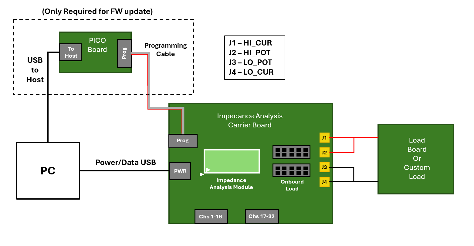
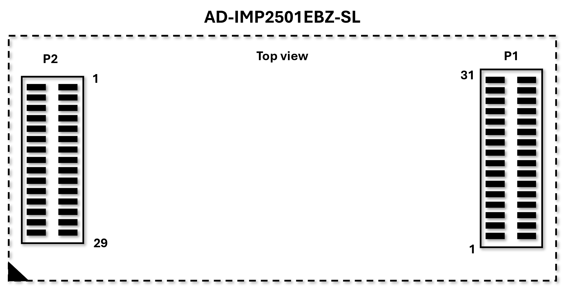
Insert the AD-IMP2501DBZ-SL module into the AD-IMP2501EBZ-SL board in the location shown above. Use the small white triangle on both the module and the carrier board to orient properly. The connectors are different sizes, so they can only be inserted in one orientation shown, but excessive force in the wrong orientation could damage the connectors.
Use the picture below and the following tables to install the correct jumpers for your desired operation. The first table is for power and general communication. The second table is for EIS on board measurements. The third table is for EIS off board measurements.
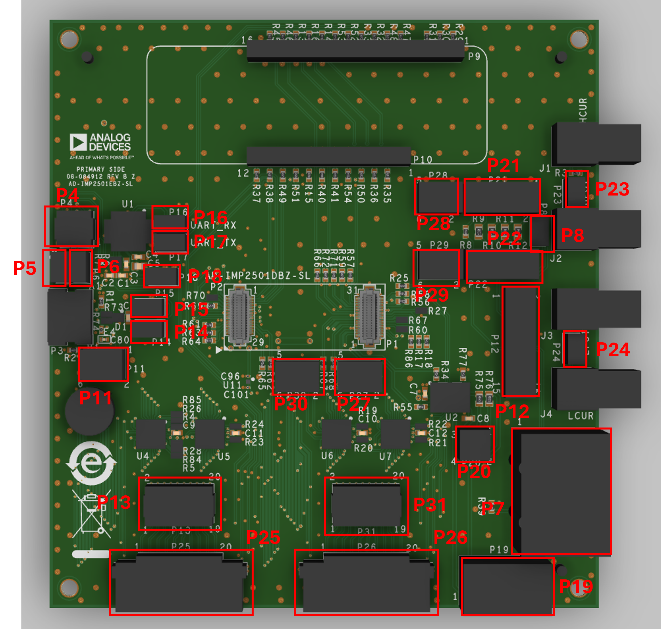
Verify jumpers are installed in the locations designated by the following table for power and communication.
Jumper Designation |
Install Position |
Description |
|---|---|---|
P4 |
Not Installed |
Programming Header |
P5 |
Not Installed |
Debug UART TX |
P6 |
Not Installed |
Debug UART RX |
P11 |
Pins 1-2 |
USB C Power Supply |
P14 |
Pins 1-2 |
USB C DM |
P15 |
Pins 1-2 |
USB C DP |
P16 |
Pins 1-2 |
FTDI UART RX |
P17 |
Pins 1-2 |
FTDI UART TX |
P18 |
Pins 1-2 |
FTDI Power |
P20 |
Not Installed |
CAN Bus |
For EIS on board measurements install jumpers according to the following table. Note that to select an onboard load, both jumpers, corresponding to the appropriate load, need to be installed. If the user selects their own component in position 8, no jumpers should be installed on P21 or P22.
Jumper Designation |
Install Position |
Description |
|---|---|---|
P27 |
Pins 1-2 |
EIS HCUR |
P28 |
Pins 1-2 |
EIS HPOT |
P29 |
Pins 1-2 |
EIS LPOT |
P30 |
Pins 1-2 |
EIS LCUR |
P23 |
Pins 1-2 |
HCUR to HPOT connection |
P24 |
Pins 1-2 |
LCUR to LPOT connection |
P21 |
Selectable: |
|
Pins 1-2 |
10k ohms |
|
Pins 3-4 |
1k ohms |
|
Pins 5-6 |
100 ohms |
|
Pins 7-8 |
10 ohms |
|
Pins 9-10 |
0 ohms |
|
P22 |
Selectable: |
|
Pins 1-2 |
10k ohms |
|
Pins 3-4 |
1k ohms |
|
Pins 5-6 |
100 ohms |
|
Pins 7-8 |
10 ohms |
|
Pins 9-10 |
0 ohms |
|
P8 |
Not Installed |
User selectable load |
P12 |
Pins 1-2 |
EIS HCUR SMA |
Pins 5-6 |
EIS HPOT SMA |
|
Pins 9-10 |
EIS LPOT SMA |
|
Pins 13-14 |
EIS LCUR SMA |
For EIS off board measurements using the SMA connectors, install jumpers according to the following table. Connect SMA cables to J1-J4, and verify no jumpers are installed on P8, P21, P22, P23, and P24.
Jumper Designation |
Install Position |
Description |
|---|---|---|
P27 |
Pins 1-2 |
EIS HCUR |
P28 |
Pins 1-2 |
EIS HPOT |
P29 |
Pins 1-2 |
EIS LPOT |
P30 |
Pins 1-2 |
EIS LCUR |
P23 |
Pins 1-2 |
HCUR to HPOT connection |
P24 |
Pins 1-2 |
LCUR to LPOT connection |
P21 |
Not Installed |
10k ohms |
1k ohms |
||
100 ohms |
||
10 ohms |
||
0 ohms |
||
P22 |
Not Installed |
10k ohms |
1k ohms |
||
100 ohms |
||
10 ohms |
||
0 ohms |
||
P8 |
Not Installed |
User selectable load |
For EIS off board measurements using the DIN connector, only change jumpers on P12 according to the following table. Connect DIN cable to P7.
Jumper Designation |
Install Position |
Description |
|---|---|---|
P12 |
Pins 3-4 |
EIS HCUR SMA |
Pins 7-8 |
EIS HPOT SMA |
|
Pins 11-12 |
EIS LPOT SMA |
|
Pins 15-16 |
EIS LCUR SMA |
Connect the USB C cable to P3 on AD-IMP2501EBZ-SL and the host PC.
An LED on the top side of the AD-IMP2501DBZ-SL should turn on, blink twice, and turn off. It should now only turn on when data is being processed.
Software User Guide
This software user guide will help the user navigate the settings and command set to properly evaluate the best impedance analysis set-up for his or her application. The number of parameters makes it impossible to show every combination, but the user will understand how each parameter affects the measurement data.
The AD-IMP2501DBZ-SL comes with pre-loaded with embedded firmware and can be used out of the box. This firmware handles communication with the host PC, setting user specified parameters, initiating signal generation, processing impedance measurement data, and reporting that information back to the user. There are a variety of measurement parameters and modes that can be configured.
Some drivers and peripheral software is required for operation. Instructions on how to download and install all necessary software or firmware is provided below.
USB Driver Installation
Note
The default communication interface to the EVAL-AD-IMP250-SL is via its USB port. Using the USB Type C cable included with the evaluation board (TTL-232R-RPI), FTDI”s Virtual COM Port (VCP) drivers must be downloaded from their website located at https://www.ftdichip.com/Drivers/VCP.htm
Installation steps:
Download the driver setup executable for the host OS version from https://www.ftdichip.com/Drivers/VCP.htm
Note: for detailed instructions, visit https://www.ftdichip.com/Support/Documents/InstallGuides.htm
Unzip the file and run the setup executable
Connect the USB cable to the PC
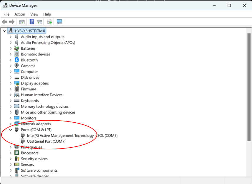
Open the Device Manager
In the Device Manager window, verify that the USB Serial Port is displayed under
Ports (COM & LPT)and that a serial port identifier has been assigned as shown below (the COM# may be different than shown here):
Embedded Software Update
If during development it becomes necessary to load new firmware onto the
AD-IMP2501DBZ-SL, follow these steps using the
MAX32625PICO2
PICO Board
Request and Download New Firmware or Software
Follow these instruction for downloading software/firmware from Analog Device”s Secure Software Delivery (SSD) system. The example below is for requesting new firmware, but the process is the same for requesting software:
A user must first make a myAnalog account by clicking
Register with emailon my.analog.com. The email used to create an account will be needed in the next step.Please contact your local ADI support or Ben Ferrara (Ben.Ferrara@analog.com) and request access to the AD-IMP2501DBZ-SL firmware or software and designate the email address used to create your myAnalog account.
You will receive an email that looks like the below image once the request has been processed. Follow the URL at the bottom of the page:
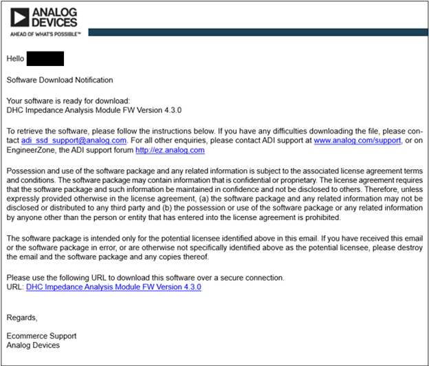
View the software license agreement by selecting the hyperlink
software
license agreement
highlighted in blue, and hit the check box to indicate that you have read and agree to the terms outlined in the license.
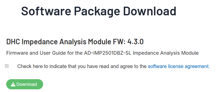
Then select the green
Downloadbutton. This will download a zipped folder containing a .hex file that can be flashed onto the AD-IMP2501DBZ-SL.
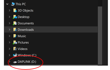
Connect the PICO board
Using a USB micro cable connect the PICO board to your host PC. Connect the programming cable to the programming header on the PICO board and the AD-IMP2501EBZ-SL board, P4, as shown in the Hardware User Guide. Use the picture in the Hardware User Guide General Setup section for locating the proper header. Once connected, open a file explorer window and verify that a DAPLINK drive has been found by your PC. See below circled in red.
Flash the ADI Provided Firmware File
Locate the firmware file that was downloaded via ADI”s SSD system in the
Installation Instruction section of this document. The file should be named with
the following convention: AD-IMP2501DBZ-SL_RX.Y.Z_B1.0 where the X.Y.Z
corresponds to the numbered revision of the firmware file.
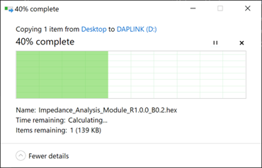
Simply drag and drop the .hex file into the DAPLINK drive and a download screen should open and show the process.
After flashing, power cycle the AD-IMP2501DBZ-SL by removing the USB C cable
from the AD-IMP2501EBZ-SL, and then reconnecting it. Check that the process was
successful by opening a terminal and using the version command. Verify the
revision the board reports is the same as the firmware file that was flashed
(more explanation on how to do this in the USING THE COMMAND LINE section).
Note
If the version reported by the AD-IMP2501DBZ-SL is not correct, the flashing process may have failed. A good check is to re-open the explorer window and check the DAPLINK drive.
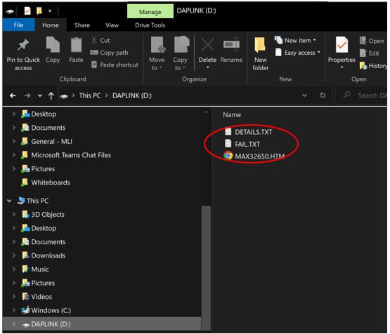
If a FAIL.TXT file exists, as shown in the image above, the FW flash was not successful. If a failure has occurred, power cycle both the PICO board and the AD-IMP2501DBZ-SL by removing the USB cables and then reconnecting them both. Attempt the download process again until successful.
Application Software
This platform utilizes multiple forms of application software. The most basic is direct communication with the AD-IMP2501DBZ-SL via the command line and a terminal emulator. This section is also where the most detail of each API command is covered.
An application GUI is also available for faster prototyping, testing, and visual data analysis.
A python script with basic command functionality is offered as a starting point for custom scripting. This script is offered for users who want to implement post processing of their data in real time or create their own visual representation of the impedance data.
AD-IMP2501DBZ-SL Available Commands
All commands should be in lower case type and each command and input value
should be separated by spaces. Only one command can be entered at a time. An
incorrect format or command that is not listed will result in the terminal
prompting the user to correct their input, or type help to review the list.
At any point, to cancel a measurement or any command that is currently running
on the system, hit Esc and the system will abort the current command and
prompt the user for a new input.
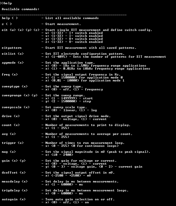
help: Typing
helpand hitting enter will display all the available commands the user can choose from. The command, followed by the necessary input/s separated by spaces. A short description of the command and inputs are provided on the left. An empty bracket< >indicates that no input is necessary other than the command itself.z: Typing
zstarts a measurement and returns impedance data to the screen. This is considered one measurement loop.eit: Typing
eitfollowed by 4 individual values defines and starts a single specific EIT measurement. The 4 individual values correspond to I+, I-, V+, and V-. I+ is the current drive, I- is the current return, V+ is the positive voltage differential measurement, and V- is the negative voltage differential measurement. Typing different values after eit will enable different switches and force the different signals through the desired path.eitpattern: Typing
eitpatternstarts EIT measurements with all the electrode patterns saved in memory from theeitlistcommand. This will iterate through all patterns and output data for each configuration.eitlist: Typing
eitlistwill prompt the user to input how many EIT measurements they would like to take. The device will then prompt the user to enter all EIT switch configurations. Each configuration should be a set of 4 values, separated by spaces, and each configuration should be separated by newlines.appmode: Typing
appmodeallows the user to select different frequency ranges for different application types. Currently, there are two ranges, 1Hz to 1.5MHz, and 0.01Hz to 10kHz. The 0.01Hz to 10kHz range is primarily untested at this point in time.freq: Typing
freqand a value between 1 and 1000000 changes the frequency parameter of the next single frequency measurement.sweeptype: Typing
sweeptypeand0disables the sweep measurement. Typing1as an input enables a frequency sweep measurement. Enabling sweeptype will utilize the sweeprange and sweepscale parameters.sweeprange: Typing
sweeprangeand two values selects the sweep range. The first value indicates the starting frequency point of the sweep and the second value indicates the ending frequency point of the sweep. The number of points between the sweep start and sweep stop will be determined by the count parameter. The spacing between points will be determined by sweepscale parameter.sweepscale: Typing
sweepscaleand0enables a linear distribution of points in the sweeprange or typing1enables a logarithmic distribution.drive: Typing
driveand0enables the voltage drive output while typing1enables the current drive output.count: Typing
countand a value between 1 and 255 sets the number of measurements to display to the screen per measurement loop. This will apply to both single frequency measurements or sweeps.avg: Typing
avgand a value between 1 and 255 sets how many measurements will be taken and then averaged for every displayed measurement.trigger: Typing
triggerand a value between 0 and 255 sets how many times to run the measurement loop. Setting trigger to 0 will enable a continuous measurement loop and will end when the user aborts by enteringESC.mag: Typing
magand a value between 20 and 2400 sets the signal magnitude in mV. This is the magnitude generated before the load and before the current limiting series resistor. The current limiting resistor is set to 100 ohms but could be changed depending on the application.gain: Typing
gainand two values. The first is either0or1to determine which channel gain should be adjusted. 0 represents the voltage receive path and 1 represents the current receive path. The second value is either 0 – 3 if the voltage gain channel was chosen or 0 – 2 if the current gain channel was chosen. These gain values will multiply the measured signal via hardware and are approximately equal to x1, x2, x4, and x8 for the voltage channel and equal to x50, x500 and x5000 for the current channel.dcoffset: Typing
dcoffsetand a value between -2500 and 2500 sets the DC voltage offset of the output signal.measdelay: Typing
measdelayand a value between 1 and 60000 sets the delay between displayed measurements in milliseconds.trigdelay: Typing
trigdelayand a value between 0 and 60000 sets the delay between displayed measurement loops in milliseconds.autogain: Typing
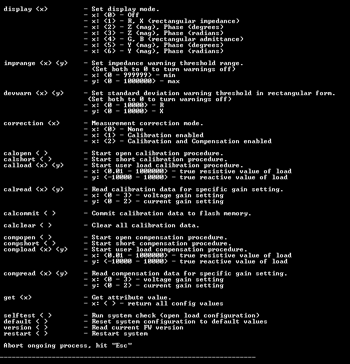
autogainand0to disable the system auto gain feature or1to enable the auto gain. When auto gain is enabled the voltage and current gain channels will be automatically selected for each measurement. It is not recommended to have auto gain turned on during frequency sweeps. There will not be a recording of which gain setting was used for each sweep measurement and it is possible that slight discrepancies between gain settings could exist. Gains will be re-evaluated and re-set after each measurement.display: Typing
displayand a value between 0 and 6 chooses the format of the displayed measurement. 0 will turn off the display. 1 will format the measurements in impedance rectangular form [R, X] (Resistance, Reactance). 2 will format the measurements in impedance magnitude and phase (in degrees). 3 will format the measurements in impedance magnitude and phase (radians). 4 will format the measurements in admittance rectangular form [G, B] (Conductance, Susceptance). 5 will format the measurements in admittance magnitude and phase (in degrees). 6 will format the measurements in admittance magnitude and phase (radians).imprange: Typing
imprangeand two values between 0 and 100000 represents the impedance warning threshold. The first value represents the minimum impedance value the user expects and the second value represents the maximum impedance value. Any measured value outside this range will cause the system to generate a warning message. Typing 0 and 0 will turn warnings off.devwarn: Typing
devwarnand two values represents the standard deviation warning. These values should be entered for measurements in rectangular form. The first value represents the deviation range ofRand second represents the deviation range ofX. This threshold will only be applied if avg is greater than 1. Typing 0 and 0 will turn warnings off.correction: Typing
correctionand a value between 0 and 2 changes the calibration setting. 0 represents no calibration applied to the measurements. 1 will apply only calibration adjustments to the measurements. 2 will apply both calibration and compensation adjustments.calopen: Typing
calopeninitiates the open calibration procedure. H_CUR and H_POT nodes should be tied together and the L_CUR and L_POT nodes should be tied together.calshort: Typing
calshortinitiates the short calibration procedure. H_CUR and H_POT nodes should be tied together with the L_CUR and L_POT nodes.calload: Typing
calloadfollowed by two values initiates the load calibration procedure. The first value represents the true resistive part of the connected load and the second value represents the true reactive part of the connected load. Connect the H_CUR and H_POT nodes to one side of the desired load and the L_CUR and L_POT nodes to the other side of the load.calread: Typing
calreadfollowed by two values reads the saved calibration values for a specific gain combination. The first value represents the voltage gain setting and the second represents the current gain setting.calcommit: Typing
calcommitsaves any calibration data that has been measured in this session to memory. Calibration data will not be saved after a power cycle if it is not committed to memory.calclear: Typing
calclearerases all saved calibration data that has been saved to memory.compopen: Typing
compopeninitiates the open compensation procedure. H_CUR and H_POT nodes should be tied together and the L_CUR and L_POT nodes should be tied together.compshort: Typing
compshortinitiates the short compensation procedure. H_CUR and H_POT nodes should be tied together with the L_CUR and L_POT nodes.compload: Typing
comploadfollowed by two values initiates the load compensation procedure. The first value represents the true resistive part of the connected load and the second value represents the true reactive part of the connected load. Connect the H_CUR and H_POT nodes to one side of the desired load and the L_CUR and L_POT nodes to the other side of the load.compread: Typing
compreadfollowed by two values reads the saved compensation values for a specific gain combination. The first value represents the voltage gain setting and the second represents the current gain setting.get: Typing
getprints the current system configuration parameters to the screen.selftest: Typing
selftestruns a system self test. The system should be set up in an open configuration with H_CUR and H_POT tied together and L_CUR and L_POT tied together with no load attached.default: Typing
defaultsets the system back to its original default configuration.version: Typing
versionreads the firmware version that is currently loaded on the module.restart: Typing
restartinternally power cycles and restarts the system. This will not change the configuration after the module comes back online.
Command Line
For command line operation and explanation of the system API, please continue here.
Terminal Emulator Installation
To communicate with AD-IMP2501DBZ-SL via its command-line interface and UART, a terminal emulator like TeraTerm is recommended. Other user preferred terminal emulators should be acceptable but may not be tested. For instruction purposes we will continue with TeraTerm.
Download
TeraTerm Download: https://github.com/TeraTermProject/teraterm/releases
Download and run the latest stable release, following the on-screen instructions.
Important
Some terminals, such as PuTTY do not support the ANSI Escape Codes which manipulate the cursor position. If the ANSI Escape Codes are not supported, the terminal may not work properly. TeraTerm supports these characters.
Opening a Session via Teraterm
Verify the COM Port that your system is connected to in the PC”s Device Manager. Check the USB Driver Installation instructions if needed.
If multiple ports are in use and you are unsure which is connected to the AD-IMP2501DBZ-SL board simply remove the USB from the computer and when the Device Manager window refreshes, note which Port is no longer in use. Plug the system USB back into your PC and that Port should again be listed.
Continue with the system powered on via USB connection to the host PC, open the TeraTerm application and choose File -> New Connection, and choose the “Serial” radio button and select “OK”.
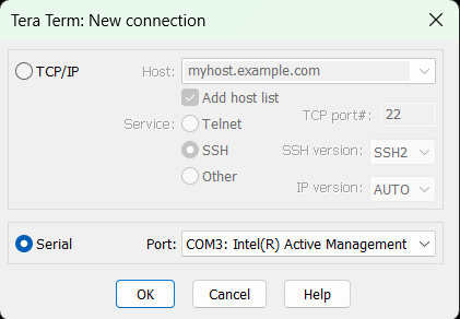
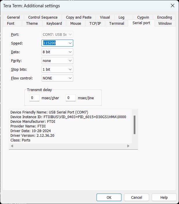
Select the COM port identified earlier in the Device Manager. Click “OK”. Then choose the tab labeled “Setup” and select “Serial port…”. Ensure that the COM port is set and the following are set accordingly, Speed = 115200, Data = 8 bits, Parity = none, Stop bits = 1 bits, Flow control = None. Then select “OK”
Optionally, choose “Setup” -> “Save setup…”. Save the file to the default directory. Now, when launching TeraTerm, it will automatically try to connect with those saved settings.
Verify the board is communicating properly by checking the following:
Press ENTER within the terminal and verify the entry
>>prompt.Type
versionand press ENTER to display the module name and firmware revision.Type
getand press ENTER to see the current parameter settings on the AD-IMP2501DBZ-SL.Type
helpand press ENTER to see a list of all commands supported by AD-IMP2501DBZ-SL.
Note that closing the TeraTerm window does not reset the AD-IMP2501DBZ-SL settings from the last session.
Using the “help” Functionality in the Command-Line Interface
The help command will display all the commands available to the user from
the command-line interface (CLI). Use this command while operating for a quick
refresher. See the AD-IMP2501DBZ-SL Available Commands
section for more details on each command.
Calibration Procedure
TBD…
Performing Basic Measurements via Command Line
Upon opening a session with TeraTerm, the AD-IMP2501DBZ-SL is ready to perform impedance measurements.
Important
The measurements reported by the module may not be accurate unless it has been calibrated. For detailed instructions on how to calibrate the module, please refer to the Calibration Procedure section in this user guide.
By default, the module is set to perform single-point impedance measurements in
rectangular coordinates with a 300mV peak-to-peak signal (magnitude = 300) at
1kHz, and no DC offset. To initiate a measurement type the z command at the
prompt and press ENTER.
Type get and press ENTER to view the current default parameter settings in
the terminal window.
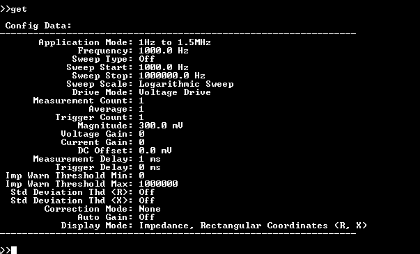
Measurement settings are not always in their base SI form. Frequency is in Hz, delays are in milliseconds. The signal magnitude sets the peak-to-peak value, centered around the offset voltage. The DC offset is in millivolts.
The AC magnitude can be configured anywhere between approximately 10mV pk-pk and 2.4V pk-pk. This represents the generated signal, but the actual magnitude across the DUT will be be dependent on the DUT impedance, due to the onboard 100Ω source resistance (for current limiting and patient protection, can be modified for different applications); see Selecting a Measurement Range for details.
Tip
The order in which the settings commands are entered is not important.
Example
Perform a 100 ohm (Jumpers on P21.5-6 and P22.5-6 in the EIS on board measurement table above) resistive measurement at 100kHz with a 1V pk-pk magnitude. Return 5 readings, displayed in Magnitude and Phase (in degrees), where each is an average of 10 samples.
>>freq 100000
 Frequency: 100000Hz

>>display 2
 Display Mode: Impedance, Magnitude and Phase in degrees (Z, deg)

>>mag 1000
 Signal Magnitude: 1000mV

>>avg 10
 Average: 10

>>count 5
 Count: 5

>>z

0, 1.024279e+02, -1.312940e+00
0, 4.878047e-02, 4.109422e-02
1, 1.024257e+02, -1.305184e+00
1, 5.721481e-02, 5.543189e-02
2, 1.024132e+02, -1.303233e+00
2, 3.633902e-02, 4.070190e-02
3, 1.024019e+02, -1.310408e+00
3, 4.281778e-02, 4.233954e-02
4, 1.023718e+02, -1.320099e+00
4, 4.378229e-02, 3.729085e-02

>>
Output is displayed as index, Magnitude, Phase (in degrees). The second line with the same index indicates the standard deviation of the averaged samples for both Magnitude and Phase of the previous measurement.
Note
By default, auto-range is not selected and the default gain channels are selected as 0 (x1 Voltage Gain) and 0 (x50 Current Gain).
Plotting Measurement Data
When acquiring multiple measurements or performing sweeps, it is useful to plot the results to observe trends or characteristics of the device under test. TeraTerm allows the user to save a log by going to File->Log, which can then be copy and pasted into a *.csv file that can be opened by spreadsheet applications such as Microsoft Excel®. The log file must be saved BEFORE taking any measurements.
To plot the acquired data in Microsoft Excel, follow the steps below:
In TeraTerm, click File, in the dropdown list select Log, and save the log file with any name and location, but make sure to change the default extension from *.log to*.csv
Select the settings desired and hit
OKConfigure the AD-IMP2501DBZ-SL and run the
zcommand to acquire the desired measurementsA separate TeraTerm window named
TeraTerm:Logwill have opened, clickCloseto stop logging dataOpen the file with Excel
Select the data to plot and insert a scatter plot to visualize the data
Graphical User Interface
TBD…
Python Script
TBD…
To facilitate easier measurement optimization on a PC, there is a library of Python functions which make it easy to operate the command-line interface from a Python script and implement a user specific set of measurements and potentially built in processing. Instead of typing commands over TeraTerm, the library accesses the Serial port directly, and calling the library functions will execute the same commands that are normally typed into the terminal emulator.
This Python library and project are currently accessible by request. Follow the instructions in the Request and Download New Firmware or Software section but request the Python Application Software for the AD-IMP2501DBZ-SL.
The Python script download includes an example measurement sweep script, which shows how to set up the Serial port, configure measurements and begin collecting data. Most functions found in the command-line interface have corresponding Python functions in the library, but not all. These functions perform a certain degree of error checking but is not complete. This library is for evaluation purposes only and is meant to be a starting point for a user to develop further.
Operation
The sections below are filled with examples and techniques on the system operation, mostly using the command line interface. The goal here is to show how different parameters may affect measurement results.
Measurement Display Modes
The AD-IMP2501DBZ-SL returns a result in one of 7 different display modes, shown
below. The result is always reported in the base SI unit. For instance,
display mode 1 (R, X) returns the impedance in rectangular form, both in
ohms.
Display Mode Number |
Mode Name |
Form |
SI Unit |
|---|---|---|---|
0 |
Display Off |
N/A |
None |
1 |
Impedance in rectangular coordinates (default) |
R, X |
Ohms, Ohms |
2 |
Impedance in magnitude and phase in degrees |
Z, deg |
Ohms, Degrees |
3 |
Impedance in magnitude and phase in radians |
Z, rad |
Ohms, Radians |
4 |
Admittance in rectangular coordinates |
G, B |
Siemens, Siemens |
5 |
Admittance in magnitude and phase in degrees |
Y, deg |
Siemens, Degrees |
6 |
Admittance in magnitude and phase in radians |
Y, rad |
Siemens, Radians |
Selecting a Measurement Range
By default, the AD-IMP2501DBZ-SL is not auto-ranging mode, and will use the default or previously set gain settings. Auto-range can be turned on which will use the highest voltage and current settings based on the frequency and magnitude of the signal.
Note
The auto-ranging algorithm is applied to each measurement. This will slow the measurement time. When performing frequency sweeps, the impedance of the device under test will change and the auto-range could detect a new setting for a later measurement than the first measurement in the sweep. These changes will not be recorded so it is not advised to use auto-range during frequency sweeps unless tested and it has been determined there are no incongruent measurement points.
In some cases, the user may want to select a specific measurement range. The
measurement range is affected by the voltage gain setting of channel 0, the
current gain setting of channel 1, and the test signal magnitude. It is
recommended to run a single measurement with autogain turned on at the
frequency of interest, (this may be multiple single measurements at the
frequency sweep limits if running planning to run a frequency sweep). After
running a single measurement, run a get command and verify the voltage and
current gain settings in the parameter list. Turn autogain off, the voltage
and current gain parameters will retain the values set during the autogain
measurement. If testing at multiple frequencies, note the gain settings for each
measurement and verify the same gain settings were chosen by the autogain
setting for each measurement. If the gain settings changed, the lowest gain
settings should be chosen for an entire sweep so the system does not saturate.
Available voltage gain values for channel 0 are listed below.
Ch0 Gain |
Max Input Voltage Range |
Gain Factor |
|---|---|---|
0 |
±2.4V |
1 |
1 |
±1.2V |
2 |
2 |
±600mV |
4 |
3 |
±300mV |
8 |
Available current gain settings and the transimpedance values associated with them are listed below.
Ch1 Gain |
Max Input Current |
Transimpedance |
|---|---|---|
0 |
24mA |
49.9Ω |
1 |
2.4mA |
499Ω |
2 |
240uA |
4.99kΩ |
Estimating the Impedance and Admittance of Capacitive and Inductive Devices
Impedance is defined as the opposition to the flow of alternating current. Admittance is the reciprocal of impedance, or how easy is for alternating current to flow. Electrical components such as resistors, capacitors and inductors have a direct relationship between their value and the expected impedance (Z):
Where f is the frequency of the signal; C, L, and R are the component values in Farads, Henries and Ohms respectively. R represents resistance and X reactance.
For admittance (Y):
Where f is the frequency of the signal; C, L, and R are the component values in Farads, Henries and Ohms respectively. G represents conductivity and B susceptance.
All components, regardless of their construction, will show a combination of resistive (conductive) and reactive (susceptive) properties. These properties can be expressed in the form of ideal electrical components combined either in series or parallel. At any given frequency, impedance/admittance can be expressed as a combination of the reactive element (capacitor or inductor) and a resistive element. The total impedance or admittance magnitude can be obtained by calculating the square-root of the sum of squares (RSS) of the two components or
To determine the best measurement range for measurement, it is necessary to estimate the impedance or admittance of the device under test at the frequency of measurement using the equations above. A simpler method to obtain an approximate value based on the expected capacitance or inductance value is through the reactance chart shown below.
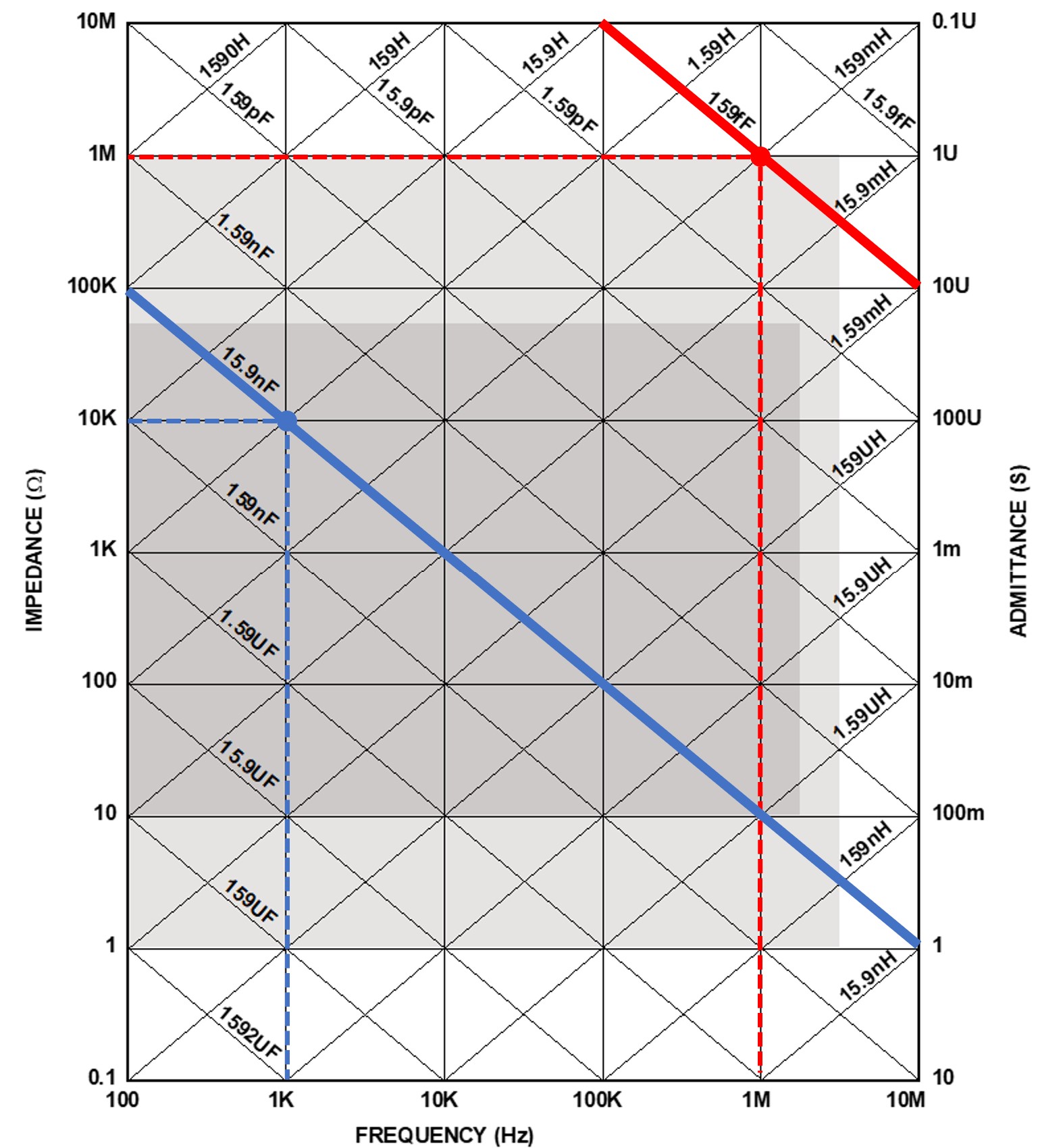
To find the approximate impedance or admittance value for a capacitor or
inductor, find the closest expected value assigned to the diagonal lines and
find its equivalent impedance/admittance value on the vertical axis at the
frequency of interest (on the horizontal axis). For example, the impedance of a
159fF capacitor, which is represented by the red solid diagonal line in the
reactance chart, exhibits |Z|=1MΩ at 1MHz, indicated by the 1M tick on the
vertical axis. This matches the estimated value using equation Z = X =
-1/(2πfC). Similarly, for a 15.9nF capacitor, which is shown as blue solid
diagonal line in the chart, |Z|=10KΩ at 1kHz.
However, depending on the DUT, it may not always be possible to estimate the
properties, which is why the experimental and testing method utilizing the
autogain feature is also recommended.
Reducing Measurement Noise
The avg command determines how many samples are averaged for each reading
returned. Averaging reduces noise and is helpful in applications that require
detecting small changes in a value or when the impedance component of interest
is small in comparison to the total impedance magnitude. The default is set to
1, which means no averaging is done.
Tip
Averaging increases the time required to return a reading. So finding the compromise between improved noise and measurement speed will depend on the application. At some point there is a limited return as the average value continues to increases. This threshold of limited return will depend on the application.
Improving Measurement Precision
To ensure precise and accurate measurements, impedance measurements should be performed with appropriate test fixtures. Measurement leads can introduce additional errors due to parasitic impedances that will vary depending on mechanical configuration and cabling.
To help ensure repeatable and stable measurements, custom-made fixtures that minimize impedance fluctuations due to mechanical configuration are recommended. To test surface-mount components, fixtures like the B+K Precision TL89S1 or the Keysight 16034G are good examples. For a full list of recommended accessories, please refer to the Optional Equipment section at the beginning of this user guide. These fixtures are not possible for all applications and some systems will require relative precision versus absolute precision.
Performing Frequency Sweeps
The AD-IMP2501DBZ-SL can automatically perform measurements that sweep the frequency parameter, enabling EIS (Electrical Impedance Spectroscopy) applications. The incremental frequency points can be spaced linearly or logarithmically within a specified range.
By default, the sweep function is off. To enable a frequency sweep, use the
sweeptype command and specify the sweep type, 1 for frequency sweep,
0 to turn off. The sweeprange command allows the user to enter the start
and end points of the sweep. Use sweepscale to choose between a linear 0
or logarithmic 1 sweep. The number of incremental points including the start
and stop points is determined by the count parameter.
Example
Perform an 11-point logarithmic frequency sweep from 1kHz to 1MHz.
>>count 11
 Count: 11

>>sweeptype 1
 Sweep Type: Frequency

>>sweeprange 1000 1000000
 Sweep Start: 1000Hz
 Sweep Stop: 1000000Hz

>>sweepscale 1
 Scale: Log

>>z

1.000000e+03, 1.031255e+02, -1.630275e-02
1.995262e+03, 1.023943e+02, -2.934620e-02
3.981072e+03, 1.025097e+02, -4.382038e-02
7.943283e+03, 1.024828e+02, -1.119833e-01
1.584893e+04, 1.024931e+02, -2.017830e-01
3.162278e+04, 1.024935e+02, -4.088743e-01
6.309575e+04, 1.024701e+02, -8.741217e-01
1.258926e+05, 1.024697e+02, -1.634526e+00
2.511887e+05, 1.026109e+02, -3.280124e+00
5.011873e+05, 1.029818e+02, -6.563277e+00
1.000000e+06, 1.043930e+02, -1.319202e+01

>>
Note
When sweeping frequency, the first value printed will be the frequency value instead of index, followed by the measurement in the display format selected.
Optimizing Measurement Timing
This section describes what settings impact the measurement time and how. The measurement time is dependent on a number of factors. Command transmission time, configured delays, source setup time, ADC acquisition time, count setting, averages, etc. Some factors, like the ADC acquisition time, are dependent on the frequency since the ADC needs to capture a minimum number of cycles of the waveform.
Delay Usage and Measurement Sequencing
The commands measdelay (measurement delay) and trigdelay (trigger delay)
can be used to control the settling time between measurements.
The measurement delay or
measdelayis observed before each measurement, but not between samples when averaging. The delay is also applied during sweeps and between multiple counts. Both the DC offset and AC test signal are enabled during the delay, but the ADCs do not capture data for the measurement until the delay has elapsed.The ideal measurement delay suitable for different DUTs may vary. When measuring a large capacitive load, consider the settling time it requires to charge; a longer measdelay is preferred to prevent accuracy loss.
Trigger delay is only observed after trigger events controlled by the
triggercommand. It is easiest to think of trigger events as measurement loops. One measurement loop could consist of multiple measurements and then repeats several times. If configured, the DC offset will be enabled during the trigger delay, but the AC source will only start after the delay for the data capture.
To setup measdelay and trigdelay, simply enter the command followed by a
value in milliseconds, up to a maximum of 60 seconds.
Below is a demonstration on how each measurement time parameter fits in the measurement sequence. Note that the sinusoidal excitation is turned on during periods marked with blocks in light/dark green. If enabled, the DC offset will turn on during the tdelay blocks. The example measurement uses a 100 Ohm onboard resistor as the DUT.
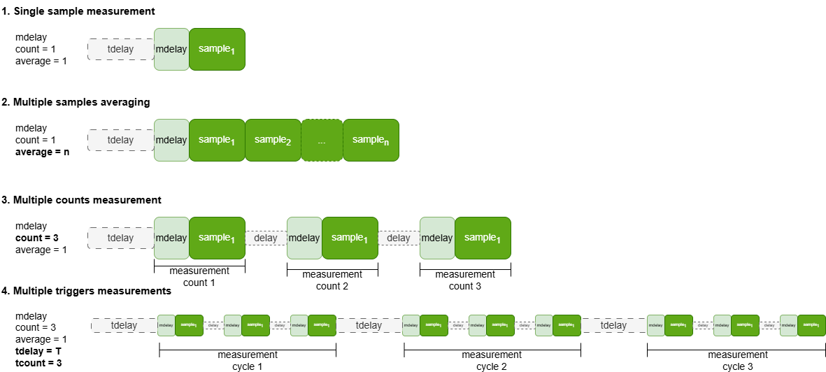
Single Sample Measurement
When measuring one sample (one count), a measdelay is observed before each
measurement where the single sample is captured.
>>count 1
 Count: 1

>>avg 1
 Average: 1

>>z

1.000000e+03, 1.022631e+02, -4.570409e-02
Single Sample with Averaging
When measuring with avg > 1, but count == 1, measdelay is observed
only before the first sample, but not between internal averaged samples. The
display now shows 2 lines after a measurement due to averaging. The second line
shows the index, the standard deviation of the first display unit, the standard
deviation of the second display unit.
>>count 1
 Count: 1

>>avg 10
 Average: 10

>>z

1.000000e+03, 1.022631e+02, -4.570409e-02
1.000000e+03, 5.502485e-01, 4.377977e-01
Multiple Samples
When measuring and displaying multiple samples (count > 1), measdelay is
observed before each measurement.
>>count 3
 Count: 3

>>avg 1
 Average: 1

>>z

0, 1.025080e+02, -6.183665e-01
1, 1.027569e+02, -1.343047e+00
2, 1.030360e+02, -3.661266e-01
Multiple Triggers
When trigger > 1, multiple measurement triggers (or measurement loops) are
enabled. A single measurement loop setting (say count = 3, avg = 1),
will be triggered trigger number of times. The trigdelay defines the
delay time between these trigger events.
>>count 3
 Count: 3

>>avg 1
 Average: 1

>>trigdelay 250
 Trigger Delay: 250ms

>>trigger 3
 Trigger Count: 3

>>z

0, 1.024911e+02, -1.148774e-01
1, 1.025547e+02, -1.195827e-01
2, 1.024493e+02, -1.660484e-01

0, 1.024618e+02, -1.313231e-01
1, 1.025220e+02, -1.391520e-01
2, 1.024505e+02, -1.339683e-01

0, 1.025001e+02, -1.355432e-01
1, 1.024866e+02, -1.084897e-01
2, 1.025063e+02, -1.583959e-01
Optimizing Single Point Measurements
To achieve the fastest single-point measurement time, there are a few points to consider.
Delays: the trigger delay
trigdelayand measurement delaymeasdelaydirectly impact the measurement time. As explained above,trigdelayis applied once per trigger loop, and themeasdelayis applied once percount(or displayed measurement sample). Therefore, a typical single measurement will havetrigdelay+measdelayadded on. The defaulttrigdelayis 0 ms; and this is recommended to optimize the measurement time. The defaultmeasdelayis 1 ms; this is restricted to a 1ms minimum as lower could cause the ADC to capture some data before the AC source has fully turned on. Increasing this value can be useful for some situations depending on the load, but does not generally lead to improved measurement data. However, it can be good practice to test with different setups.Autogain: the
autogainfeature should be disabled for the fastest measurements. Theautogaintests the ideal gain by taking multiple measurements with different gain settings, and checking for ADC saturation. This can significantly increase the measurement time.Averaging: adding more averaging increases the number of samples taken and averaged together per measurement
count, which can significantly add time between each displayed value. This can increase measurement time but it will reduce the per sample time when compared to taking individual samples and averaging them together post measurement. An example times are shown in the table below.Frequency: the measurement time is highly dependent on the test frequency. The system tries to capture a specific number of data points of the signal waveform for a more accurate measurement. Generally, frequencies above 1kHz this impact becomes minimized.
Display mode: the measurement can be slightly slower if not using the rectangular format. Less processing is required when not converting from rectangular coordinates such as display mode 1 (R, X). Modes with angle in degrees or radians (polar form) can take slightly longer, but usually the effect is negligible.
Calibration/Compensation: turning on different calibration/compensation modes can cause added delays as well but similar to the display mode, the effect is negligible. More processing is required to apply calibration/compensation models to measured data. The delay is microseconds, up to 100”s of microseconds.
This table shows various timing measurements at different frequencies with different parameter settings. Some timings could change slightly depending on frequency, setup, or different with combinations of parameters, but this table should give a good estimate of the impact of different parameter settings. The average time is calculated as how long an individual sample took when either there were multiple samples being averaged together or multiple samples being displayed as one measurement loop. The delta time is the comparison of a measurement to the same frequency under ideal parameters in the first few rows.
Freq (Hz) |
# Samples |
Avg |
Meas Delay (ms) |
Display |
Cal/Comp |
Auto Gain |
Time (s) |
Avg Time (s) |
Δ Time (s) |
|---|---|---|---|---|---|---|---|---|---|
1000000 |
1 |
1 |
1 |
R/X |
None |
Off |
0.00544 |
NA |
NA |
100000 |
1 |
1 |
1 |
R/X |
None |
Off |
0.00461 |
NA |
NA |
10000 |
1 |
1 |
1 |
R/X |
None |
Off |
0.00445 |
NA |
NA |
1000 |
1 |
1 |
1 |
R/X |
None |
Off |
0.00489 |
NA |
NA |
100 |
1 |
1 |
1 |
R/X |
None |
Off |
0.01439 |
NA |
NA |
10 |
1 |
1 |
1 |
R/X |
None |
Off |
0.10454 |
NA |
NA |
1 |
1 |
1 |
1 |
R/X |
None |
Off |
1.014 |
NA |
NA |
1000000 |
1 |
10 |
1 |
R/X |
None |
Off |
0.02333 |
0.002333 |
-0.003107 |
100000 |
1 |
10 |
1 |
R/X |
None |
Off |
0.01516 |
0.001516 |
-0.003094 |
10000 |
1 |
10 |
1 |
R/X |
None |
Off |
0.01354 |
0.001354 |
-0.003096 |
1000 |
1 |
10 |
1 |
R/X |
None |
Off |
0.01813 |
0.001813 |
-0.003077 |
100 |
1 |
10 |
1 |
R/X |
None |
Off |
0.10954 |
0.010954 |
-0.003436 |
10 |
1 |
10 |
1 |
R/X |
None |
Off |
1.015 |
0.1015 |
-0.003040 |
1 |
1 |
10 |
1 |
R/X |
None |
Off |
10.119 |
1.0119 |
-0.002100 |
10000 |
1 |
1 |
10 |
R/X |
None |
Off |
0.01345 |
NA |
0.009000 |
1000 |
1 |
1 |
10 |
R/X |
None |
Off |
0.01393 |
NA |
0.009040 |
10000 |
1 |
1 |
1 |
Z/Deg |
None |
Off |
0.00451 |
NA |
0.000060 |
1000 |
1 |
1 |
1 |
Z/Deg |
None |
Off |
0.00496 |
NA |
0.000070 |
10000 |
1 |
1 |
1 |
R/X |
None |
On |
0.03499 |
NA |
0.030540 |
1000 |
1 |
1 |
1 |
R/X |
None |
On |
0.03803 |
NA |
0.033140 |
10000 |
1 |
1 |
1 |
R/X |
Cal |
Off |
0.00449 |
NA |
0.000040 |
1000 |
1 |
1 |
1 |
R/X |
Cal |
Off |
0.00489 |
NA |
0.000000 |
10000 |
1 |
1 |
1 |
R/X |
Cal/Comp |
Off |
0.00456 |
NA |
0.000110 |
1000 |
1 |
1 |
1 |
R/X |
Cal/Comp |
Off |
0.00502 |
NA |
0.000130 |
10000 |
10 |
1 |
1 |
R/X |
None |
Off |
0.03904 |
0.003904 |
-0.000546 |
1000 |
10 |
1 |
1 |
R/X |
None |
Off |
0.04343 |
0.004343 |
-0.000547 |
Calibration and Compensation
A few milliseconds after power up, the AD-IMP2501DBZ-SL is ready to perform measurements. However, any readings and their units are scaled and assigned using nominal circuit parameters. Measurement accuracy should only be evaluated after performing calibration on the module. Using an external calibration source with certified traceability. For example, the Keysight E4980A can be used to validate.
There are three basic calibration steps involved in calibrating the module: open calibration, short calibration, and load calibration. The first two correct the module and test lead parasitics. The latter provides traceability to an external source. The calibration steps must be performed in the order open->short->load. Open and load calibration are the most important. Short calibration may need to be skipped in certain gain/load ranges where the current ADC would saturate. Open calibration may need to be skipped in gain/load ranges that the voltage ADC would saturate.
Tip
When performing load calibration for a given gain setting, the optimal load device (usually a resistor) is one with an impedance magnitude close to that of the eventual load impedance. This will give the best system accuracy.
Resistors, capacitors or inductors can be used for calibration. High-quality resistors (e.g. thin film or metal film), air capacitors, and gas-filled capacitors tend to provide the best results. Alternatively, C0G/NP0 type ceramic capacitors can be used as well. The true value of these components should be determined with traceable measurements from another meter, such as the Keysight E4980A.
Each measurement configuration (ch0 and ch1 gain combination) needs to be calibrated separately. If calibration is performed for only one gain combination, calibration needs to be carried out again if the gain configuration changes. There are a total of 12 possible gain combinations based on the 4 gain and 3 transimpedance settings for channel 0 (voltage) and channel 1 (current) respectively.
If the user calibrates at a specific gain, then changes the load and calibrates again, the user will overwrite the result of the first calibration. Support for calibration over frequency is included and incorporates the entire 1Hz to 1.5MHz range.
Calibration Steps
To calibrate the module in a specific gain combination, follow the steps below:
Select the desired measurement configuration (gain, magnitude, and offset)
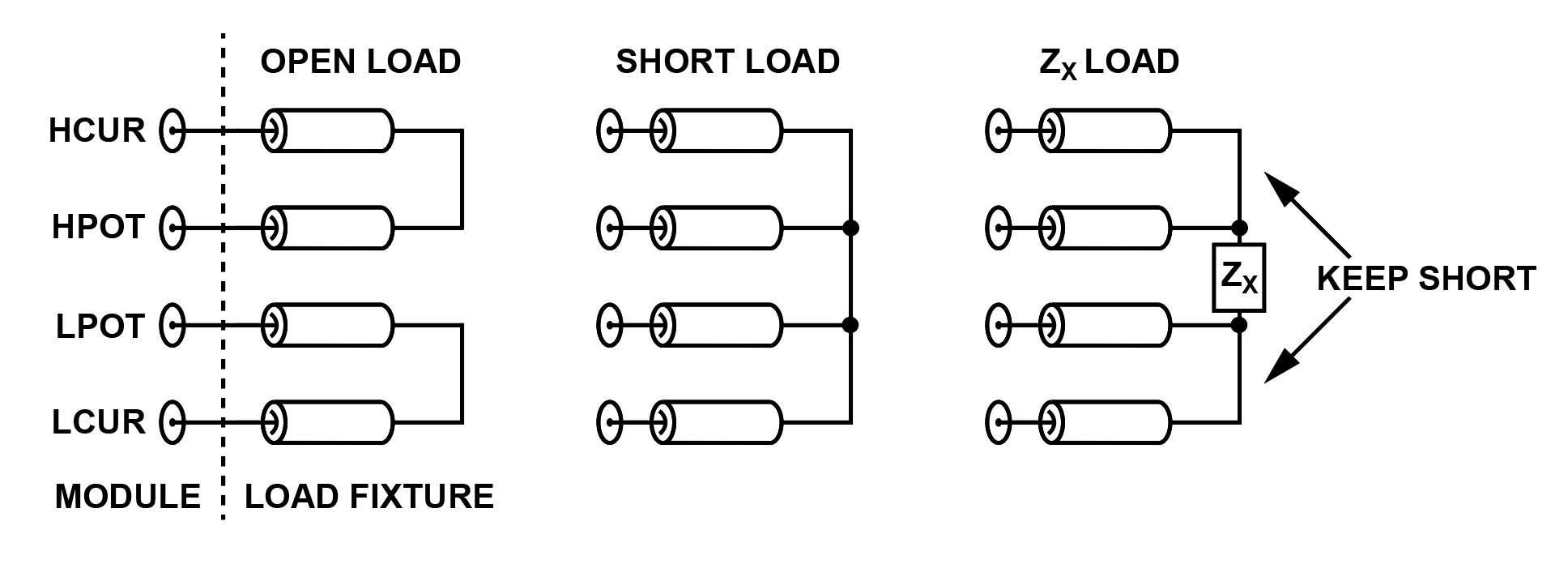
Connect the H_POT and H_CUR terminal together and the L_POT and L_CUR terminals together to form two separate connection pairs
If using the on board loads, apply the jumpers as designated below:
Jumper Designation |
Install Position |
Description |
|---|---|---|
P27 |
Pins 1-2 |
EIS HCUR |
P28 |
Pins 1-2 |
EIS HPOT |
P29 |
Pins 1-2 |
EIS LPOT |
P30 |
Pins 1-2 |
EIS LCUR |
P23 |
Pins 1-2 |
HCUR to HPOT connection |
P24 |
Pins 1-2 |
LCUR to LPOT connection |
P21 |
Not Installed |
User Selectable Load |
P22 |
Not Installed |
User Selectable Load |
P8 |
Not Installed |
User Selectable Load |
P12 |
Pins 1-2 |
EIS HCUR SMA |
Pins 5-6 |
EIS HPOT SMA |
|
Pins 9-10 |
EIS LPOT SMA |
|
Pins 13-14 |
EIS LCUR SMA |
If using test clips or SMA cables that are tied together at the clip, remove jumpers from P23 and P24. Place them so the clips are separated as close to the same distance as they will be when the DUT is connected.
Note
Open calibration at high frequencies and in higher impedance measurement ranges is especially susceptible to error, due to the increased opportunity for coupling into the current measurement path. The test setup is especially important under these conditions
Run the
calopencommand and follow the prompts when ready.Connect all the measurement terminals together.
When measuring very small impedances, short calibration becomes extremely important. Many fixtures have a low repeatability under these conditions. Optimizing the repeatability of the setup is critical to getting a meaningful result, for both calibration and measurement.
In some instances
calopenorcalshortcannot be run due to the gain or magnitude setting with the desired load. In this instance, do not run the command, the system will use the default values. Alternatively, consider a different gain combination for that desired load.
Run the
calshortcommand, if possible, and follow the prompts when ready.Connect a known impedance between the measurement leads or choose a connection configuration from the on board resistors.
Run the
calload <value1> <value2>command where<value1>is the true resistive value of the component (Ohms) and<value 2>is the true reactive value of the component (Ohms) and follow the prompts when ready.To obtain true values of resistive and reactive components beforehand, use a calibrated LCR meter and select Rs and X for the display mode.
For improved results, a standard resistor set like the Keysight 42030A can be used.
After completing the steps above, calibration coefficients are generated and
stored in RAM. These coefficients will be applied to any subsequent measurements
when that gain combination is applied and the calibration is enabled, but will
be lost after a power cycle or reset of the module. To store the coefficients in
non-volatile memory (flash) the command calcommit must be executed. For
example:
>>calcommit
 Are you sure you want to commit the current calibration data to memory!?

 Press Y/y when ready to proceed or N/n to cancel.
>>y
 Calibration data committed to memory...
>>
This will store the calibration coefficients in RAM to flash. Power loss will no longer remove the stored calibration data.
Note
This commit of calibration data does not need to be done immediately after running the calibration. As long as it is completed before the next power loss the data will be saved. Multiple gain combination calibrations can be completed before committing all the data to non-volatile memory.
Calibration Example
Calibrate the gain setting (0, 1) with a resistor of value 100 Ohms. The true resistance Rt from the E4980A at 100kHz was measured as 1000.019 Ohms, and the true reactance Xt was 0.822 Ohms.
>>gain 0 0
 Voltage Gain: x1

>>gain 1 1
 Current Gain: x500

>>mag 300
 Signal Magnitude: 300mV

>>dcoffset 0
 DC Offset: 0mV

>>calopen

 Beginning open load calibration... Connect the H_POT and H_CUR together and the L_POT and L_CUR together.

 Then hit Y/y when ready to proceed or N/n to cancel.        <--- Connect open load now

>>y

 Beginning Calibration...

 Calibration Stage Completed...

>>calshort

 Beginning short load calibration... Connect all the measurement terminals together.

 Then hit Y/y when ready to proceed or N/n to cancel.        <--- Connect short load now

>>y

 Beginning Calibration...

 Calibration Stage Completed...

>>calload 100 0

 Beginning user load calibration... Connect known impedance between the measurements leads.

 Then hit Y/y when ready to proceed or N/n to cancel.        <--- Connect calibration load now (100Ω on board resistor)

>>y

 Beginning Calibration...

 Calibration Stage Completed...

>>calread 0 1

 Calibration Data
--------------------------
  R Gain Coeff: -2.409224e+06
  X Gain Coeff: 5.887465e+06
  R Open Coeff: 2.458235e+06
  X Open Coeff: -6.021623e+06
 R Short Coeff: 1.214380e-02
 X Short Coeff: -4.682108e-03
  G Gain Coeff: -7.332180e+01
  B Gain Coeff: -2.819907e+01
  G Open Coeff: 5.811038e-08
  B Open Coeff: 1.423455e-07
 G Short Coeff: 7.168965e+01
 B Short Coeff: 2.764033e+01
--------------------------

>>calcommit

 Are you sure you want to commit the current calibration data to memory!?

 Press Y/y when ready to proceed or N/n to cancel.

>>y

 Calibration data committed to memory...

>>count 5        <--- simply for more samples
 Count: 5

>>z        <--- measurement with no calibration enabled

0, 1.013174e+02, 6.936672e-01
1, 1.016581e+02, 1.105903e+00
2, 1.030758e+02, -1.493440e-01
3, 1.010275e+02, 9.489138e-02
4, 1.036238e+02, -3.363047e-01

>>correction 1
 Correction Mode: Calibration Enabled

>>z

0, 9.975729e+01, -5.334712e-01
1, 1.005431e+02, 2.199431e-01
2, 1.001880e+02, -5.269702e-01
3, 1.004466e+02, 1.122557e+00
4, 9.954122e+01, -1.490209e-01

>>
Reading Calibration Coefficients
Calibration coefficients for each gain can be read to the terminal. To read the
currently loaded coefficients for a certain gain setting, run the command
calread <vgain> <igain>. This prints the 12 AC coefficients to the terminal,
where they could be noted for future reference. If the gain combination has not
been calibrated yet, the default values will be shown.
>>calread 0 1

 Calibration Data
--------------------------
  R Gain Coeff: -2.409224e+06
  X Gain Coeff: 5.887465e+06
  R Open Coeff: 2.458235e+06
  X Open Coeff: -6.021623e+06
 R Short Coeff: 1.214380e-02
 X Short Coeff: -4.682108e-03
  G Gain Coeff: -7.332180e+01
  B Gain Coeff: -2.819907e+01
  G Open Coeff: 5.811038e-08
  B Open Coeff: 1.423455e-07
 G Short Coeff: 7.168965e+01
 B Short Coeff: 2.764033e+01
--------------------------

>>calread 1 0

 Calibration Data
--------------------------
  R Gain Coeff: -1.000000e+06
  X Gain Coeff: -1.000000e+06
  R Open Coeff: 1.000000e+06
  X Open Coeff: 1.000000e+06
 R Short Coeff: 0.000000e+00
 X Short Coeff: 0.000000e+00
  G Gain Coeff: -1.000000e+06
  B Gain Coeff: -1.000000e+06
  G Open Coeff: 0.000000e+00
  B Open Coeff: 0.000000e+00
 G Short Coeff: 1.000000e+06
 B Short Coeff: 1.000000e+06
--------------------------

>>
All gain combinations that will be utilized should be configured, otherwise the
default coefficients will be used even if calibration is turned on. Coefficients
must be saved using calcommit; otherwise, they will be lost if the system
reboots or loses power.
Compensation Procedure
Compensation is an additional measurement adjustment function designed to account for changes in the test fixture or application setup that were not present during calibration. This feature is useable, but it is also reasonable to recalibrate for each fixture/setup, and use the commands detailed in Calibration Steps to save data for each config.
To configure compensation coefficients, run the same steps in the calibration
procedure, but use the comp commands instead of the cal commands. Make
sure the commands are run with the setup fully intact and all connections to the
DUT in place. Refer to the help section on available commands for the specific
list and associated names for compensation located at
AD-IMP2501DBZ-SL Available Commands
Firmware Release Highlights
Currently available firmare versions and release highlights:
Version |
Status |
Release Highlights |
|---|---|---|
4.3.1 |
Stable |
First web release |
Support
For support, general questions, or firmware update help, reach out to your local ADI support team or email imp2501-support@analog.com.