AD-FMCMOTCON1-EBZ Controller Board
Warning
The AD-FMCMOTCON1-EBZ is a legacy product and is no longer actively supported. This documentation is provided for reference only.
Features and Block Diagram
Compatible with all Xilinx FPGA platforms with FMC LPC or HPC connectors
2x Gbit Ethernet PHYs for high-speed industrial communication
Hall, Differential Hall, Encoder, and Resolver interfaces
Current and voltage measurement using isolated ADCs
Xilinx XADC interface
Fully isolated control and feedback signals
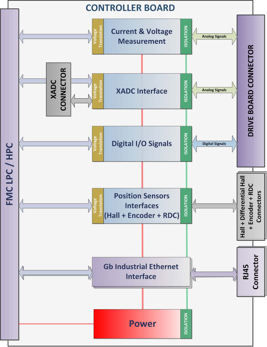
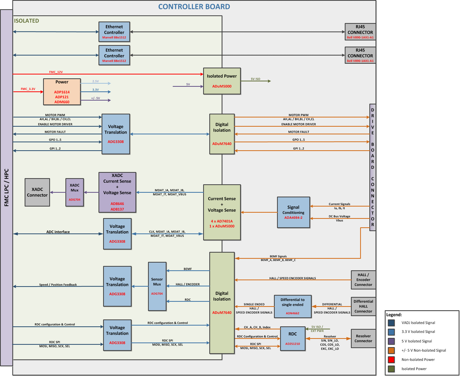
Picture and Main Components
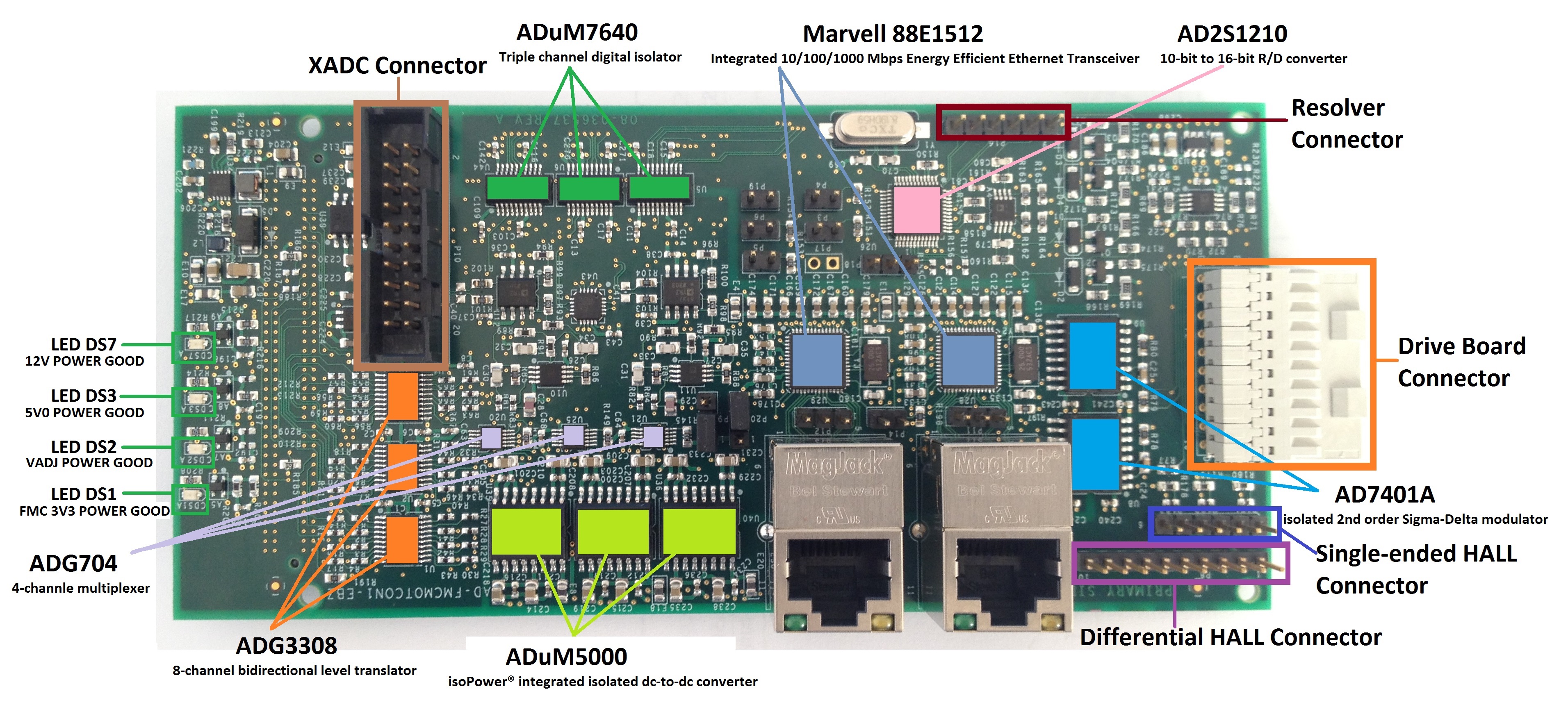
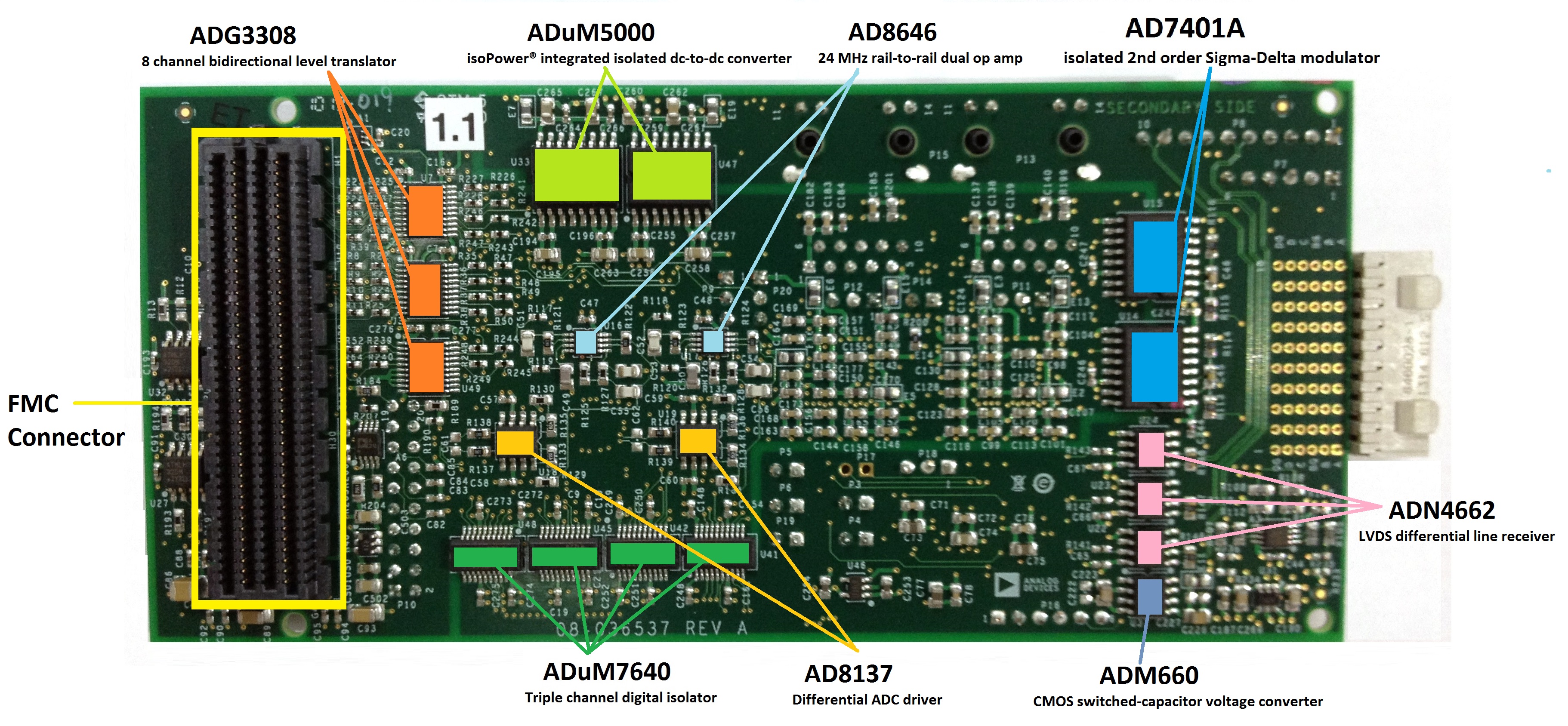
Key Parts
Part |
Description |
|---|---|
Measurement |
|
5 kV rms, isolated 2nd order Sigma-Delta modulator |
|
30 V, low noise, rail-to-rail I/O, low power operational amplifier |
|
24 MHz rail-to-rail dual op amp |
|
Variable resolution, 10-bit to 16-bit R/D converter with reference oscillator |
|
Power |
|
isoPower® integrated isolated dc-to-dc converter |
|
1000 mA, 2.5 MHz buck-boost dc-to-dc converter |
|
CMOS switched-capacitor voltage converter |
|
Isolation |
|
Triple channel digital isolator |
|
Voltage Translation |
|
8-channel bidirectional level translator |
|
Multiplexers |
|
CMOS, low voltage 2.5 Ω 4-channel multiplexer |
|
CMOS low voltage, 3 Ω 4-channel multiplexer |
|
High Speed Communication |
|
88E1512 |
Marvell integrated 10/100/1000 Mbps energy efficient Ethernet transceiver |
Jumper Settings
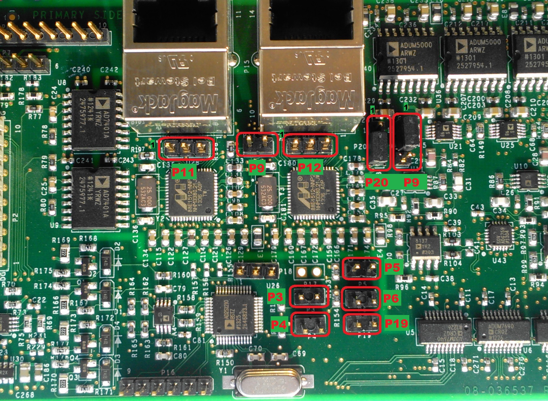
Setting |
Jumper / Position 1 |
Jumper / Position 2 |
|---|---|---|
Sensor Selection |
||
Back EMF |
P9 - position 0 |
P20 - position 0 |
Single ended Hall |
P9 - position 1 |
P20 - position 0 |
Differential Hall |
P9 - position 0 |
P20 - position 1 |
Reserved |
P9 - position 1 |
P20 - position 1 |
Resolver Configuration Mode |
||
Normal Mode - Position input |
P3 - Not inserted |
P5 - Not inserted |
Normal Mode - Velocity input |
P3 - Not inserted |
P5 - Inserted |
Reserved |
P3 - Inserted |
P5 - Not inserted |
Configuration Mode |
P3 - Inserted |
P5 - Inserted |
Resolver Resolution Settings |
||
10 Bits |
P4 - Not inserted |
P6 - Not inserted |
12 Bits |
P4 - Not inserted |
P6 - Inserted |
14 Bits |
P4 - Inserted |
P6 - Not inserted |
16 Bits |
P4 - Inserted |
P6 - Inserted |
PHYs Configuration |
||
2.5V VDDO, different PHY addresses |
P11 & P12 - Position 0 |
P9 - Inserted |
LEDs
LED |
Description |
|---|---|
DS1 |
FMC 3.3V Power Good |
DS2 |
Vadj Power Good |
DS3 |
5V Power Good |
DS7 |
12V Power Good |
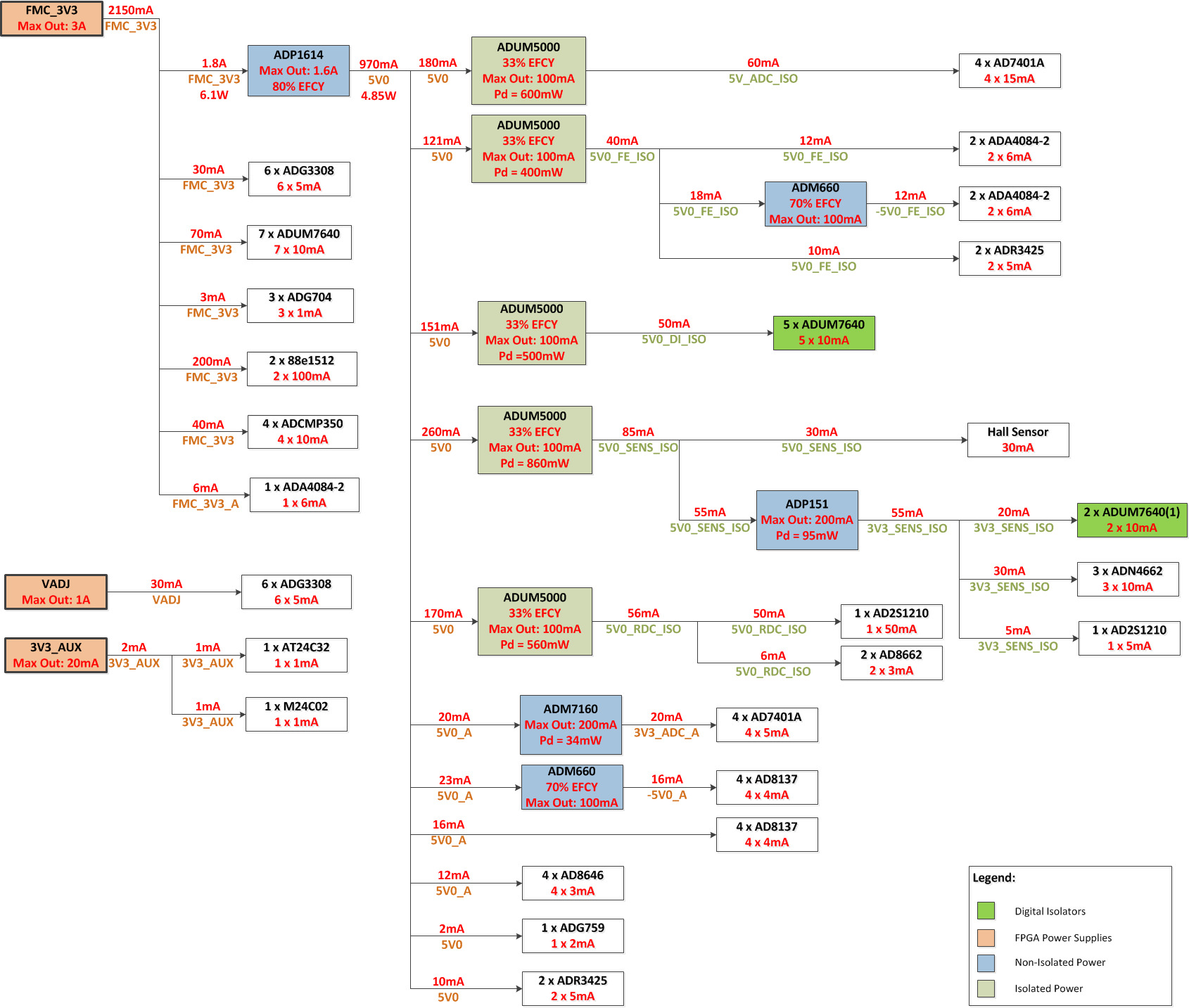
Power Map
ADC FPGA Interface
The AD7401 isolated Sigma-Delta modulators present on the controller board have a 2-wire signal interface with the FPGA:
10 / 20 MHz clock input
1-bit digital data stream output
The reconstruction of the data provided by the AD7401 modulator can be done using a SINC3 filter. A filter model and HDL implementation are provided in the AD7401 datasheet. Typical filter output characteristics:
Output code: 16-bit
Sampling rate: 78 kHz
The output code resolution and sampling rate can be controlled by changing the filter’s model and decimation. Polyphase interpolation filters are utilized to increase the sampling rate of the system.
Position & Speed Sensors FPGA Interface
Single digital interface for multiple position sensors
Single Ended HALL
Differential HALL
BEMF
Encoder
3 digital signals between hardware and the FPGA
HALL A / BEMF A / Encoder Channel A
HALL B / BEMF B / Encoder Channel B
HALL C / BEMF C / Encoder Index
Sensor selection is done with jumpers on the controller board. The hardware conditions the analog signals and sends clean digital signals to the FPGA.