LO generation options
The 2-24 GHz RF front end has two different sets of LO specifications and requirements - one for the fixed LO sources and a second for the wideband, tunable LOs. Additionally, LO performance requirements vary widely across the instrumentation, communications, and aerospace & defense application space, so while a one-size-fits-all solution for the LO generation circuitry may not be practical, Analog Devices offers numerous, flexible options for wideband frequency synthesizers.
Fixed LO source
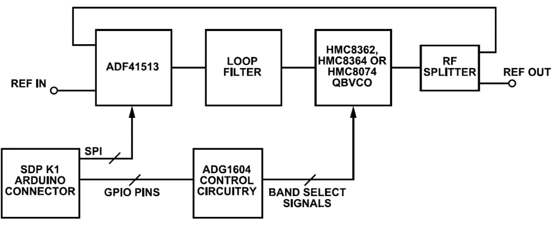
The 18 GHz, fixed LO source can be supplied by any integrated PLL/VCO such as the ADF4371, or a discrete LO implementation using ADI PLLs and quad-band VCOs for applications requiring lower phase noise. The frequency synthesizer circuit detailed in CN0568 (shown below), provides one possible solution for a discrete LO implementation using the ADF41513 PLL and HMC8362 quad-band VCO.
More information on the CN0568 frequency synthesizer can be found on the CN0568 reference design page.
This circuit was adapted to provide a cleaner output tone (reduced spurs) and a higher output power with the following block diagram:

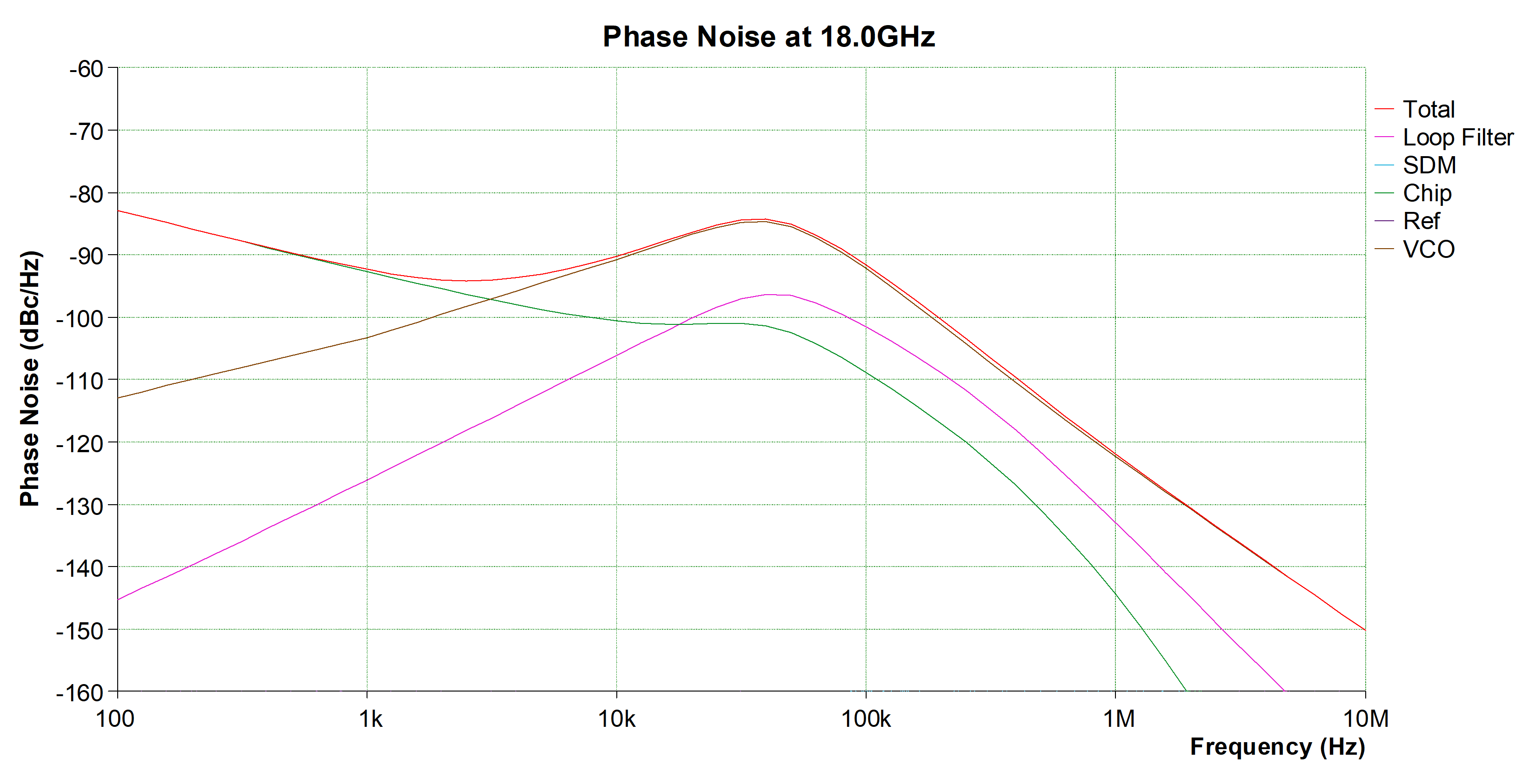
For this design, we selected a discrete LO implementation using the ADF41513 and the HMC8362 to achieve lower phase noise and power consumption. The following plot shows the simulated phase noise performance in ADI SimPLL:
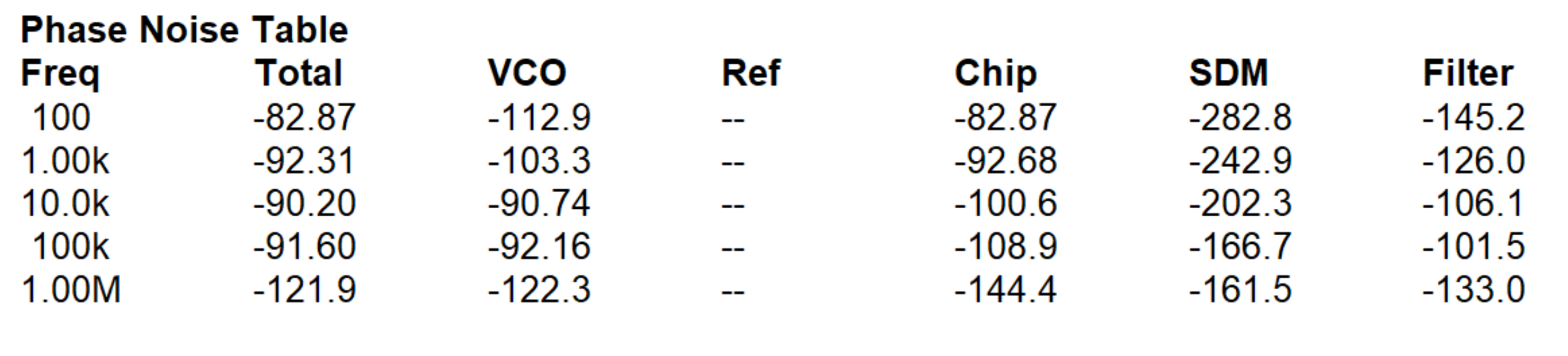
The following table summarizes the data in the plot above:
The full simulation file created in ADI SimPLL is available on request, see Requesting design files.
Tunable LO source
The tunable LO synthesizer has a more complex set of requirements, many of which directly impact the system-level functionality of the signal chain, such as tuning speed and frequency coverage. The wideband frequency synthesizer circuit shown in the figure below uses the ADF4371 integrated PLL/VCO, which is one potential option for the tunable LO source, enabling low phase-noise tuning across the RF signal chain’s full operating range. The tunable filtering on the ADF4371 outputs is optional and dependent on the LO spurious requirements of the end system. The SPDT switch selects between the two ADF4371 outputs and the HMC383 driver amp ensures sufficient LO drive level at the mixer for optimal performance.

The following plot shows the simulated phase noise performance of the tunable LO circuit for the 11.5-16 GHz output of the ADF4371 in ADI SimPLL:
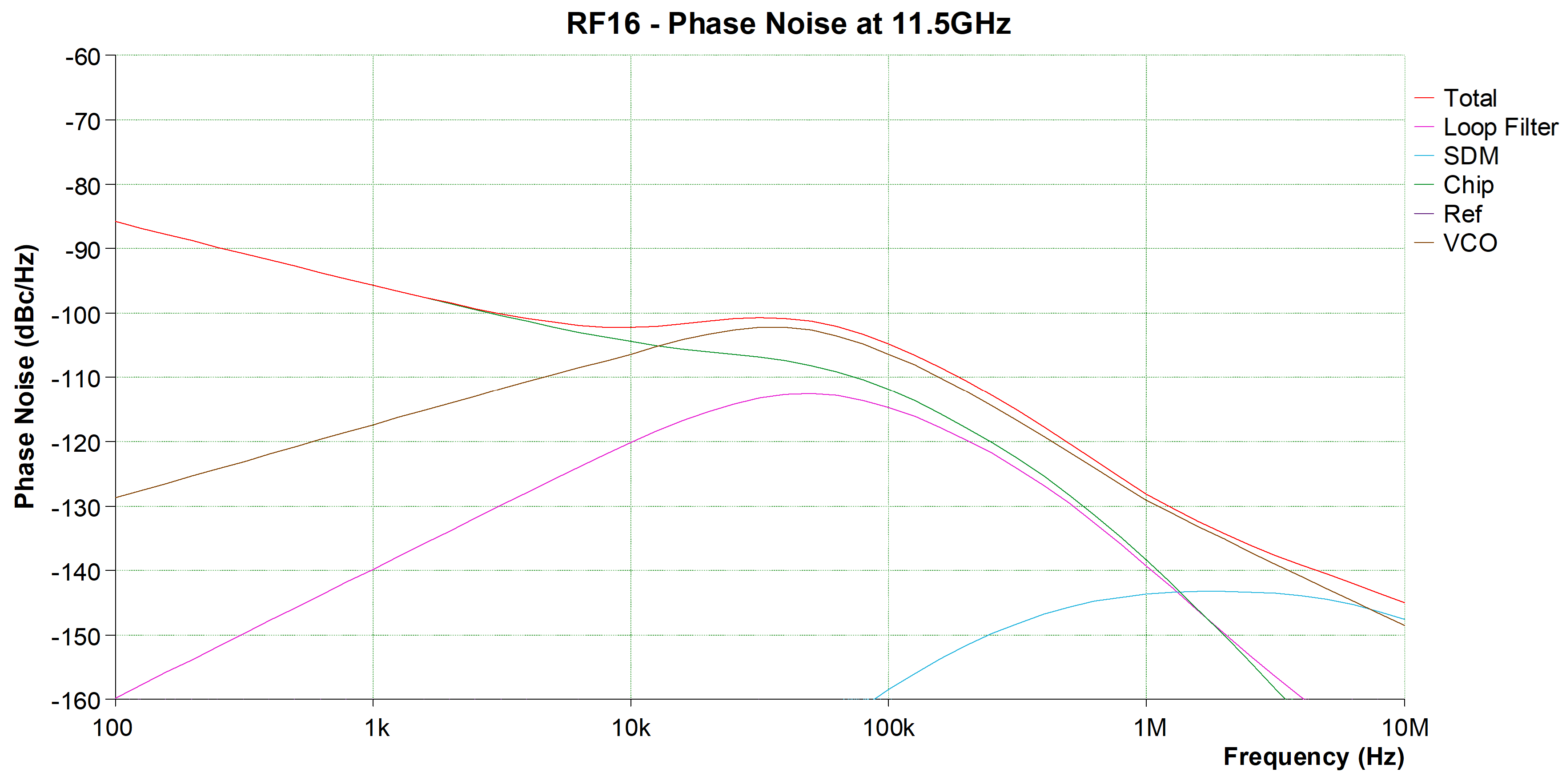
Figure 6 Tunable LO simulated phase noise, 11.5-16 GHz output
The following table summarizes the data in the plot above:

Figure 7 Tunable LO simulated phase noise summary, 11.5-16 GHz output
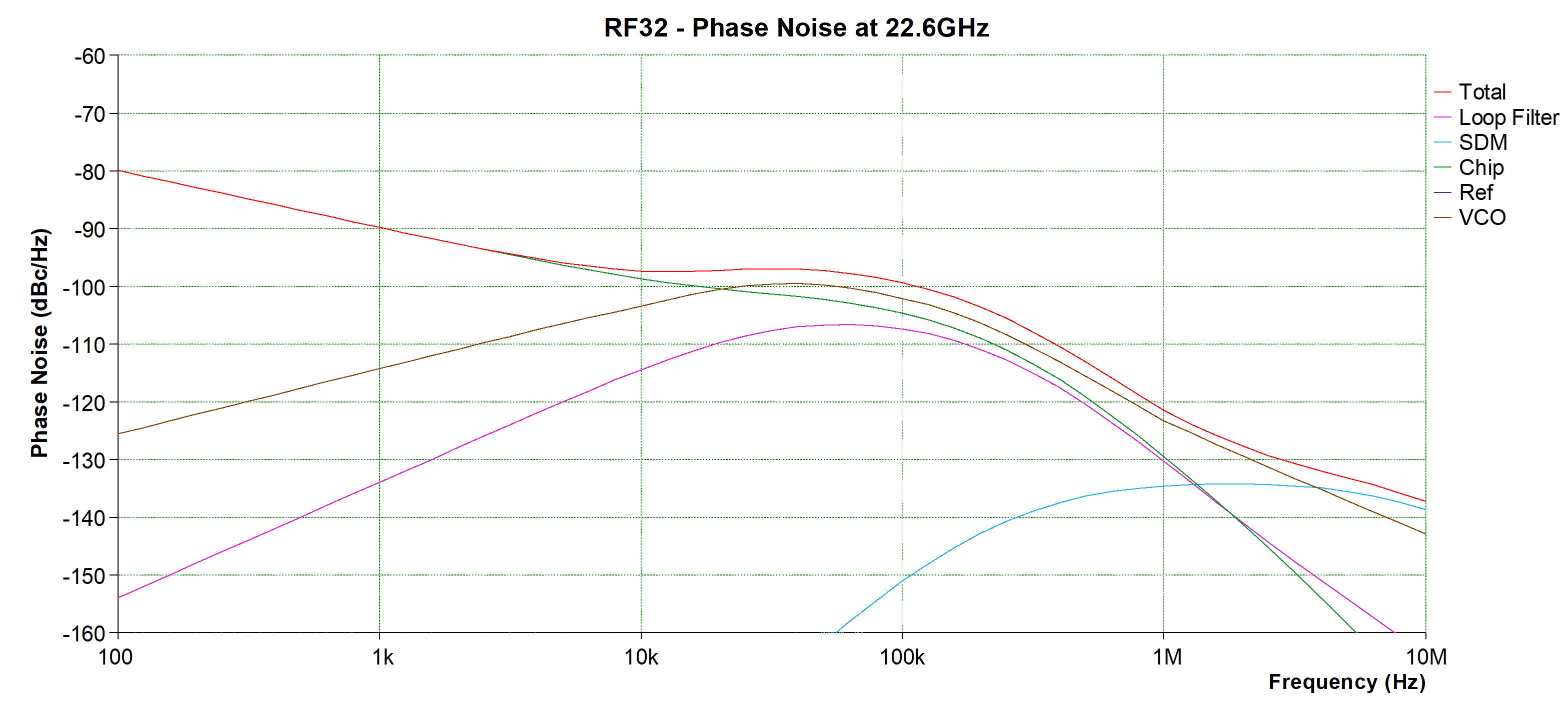
The following plot shows the simulated phase noise performance of the tunable LO circuit for the 16-28 GHz output of the ADF4371 in ADI SimPLL:
The following table summarizes the data in the plot above:
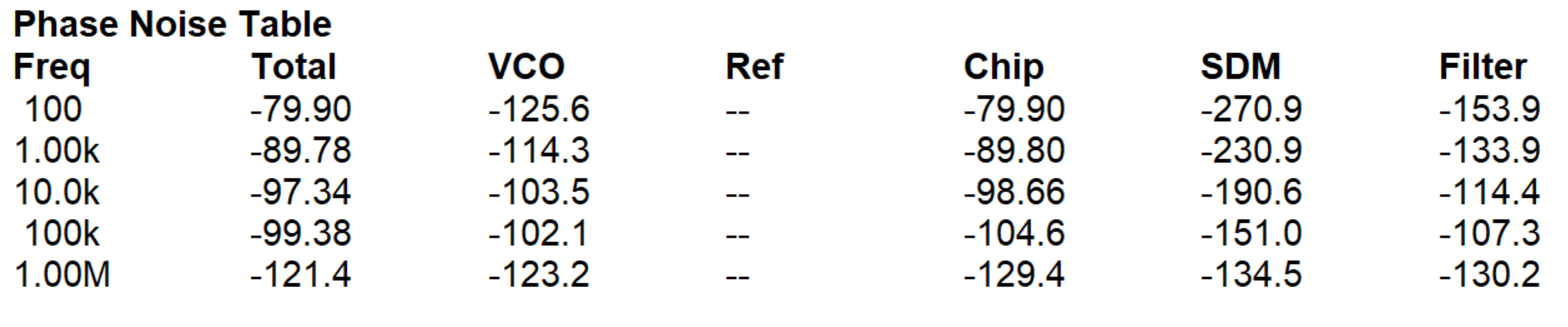
Figure 9 Tunable LO simulated phase noise summary, 16-28 GHz output
Simulation files have been created for these circuits in ADI SimPLL, one for each output of the ADF4371. These, together with the fixed LO simulation file, are available on request, see Requesting design files.