Bring-up guide
Software setup
HDL/Image
See Necessary files for the list of required boot files and build instructions.
Once built, copy the resulting files to a folder on the desktop called QuadMxFE (this directory will be used in XSCT).
IIO Oscilloscope / LibIIO
The main IIO interface is provided in the install of IIO Oscilloscope which uses LibIIO to communicate through IIO to the chips on the Quad MxFE board. The install process for IIO Oscilloscope and a walkthrough of opening the program can be found here: IIO Oscilloscope.
PuTTY
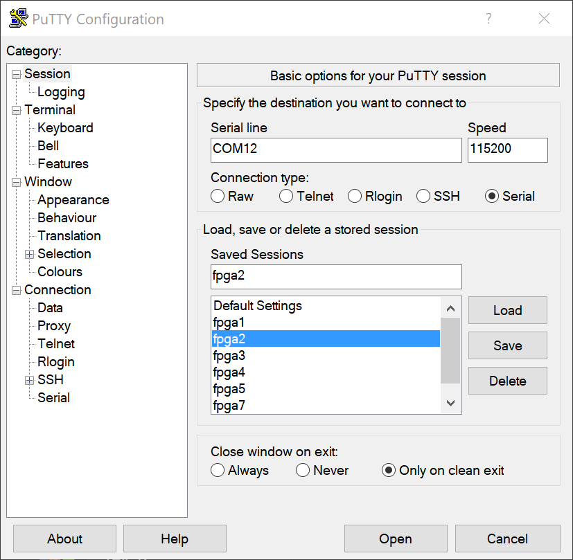
PuTTY helps to provide a view into the Linux and give additional controls and debug abilities. Putty can be downloaded from here Putty Download Page. Ensure that the proper version for the computer is downloaded (64 bit for a 64 bit PC). Once downloaded the COM port to the FPGA can be opened. This COM port can be identified through the device manager as the standard COM port:

In PuTTY, this should be opened with a baudrate of 115200.
Xilinx Software Command Line Tool (XSCT)
In order to program the FPGA, the Vitis/Vivado tool suite is required: Vivado Toolchain.
Grab the Self Extracting Web Installer from the full product installation section and run the installer. Choose the Vitis installation option which will include the Vivado install. Check the HDL build documentation for the required Vivado version.
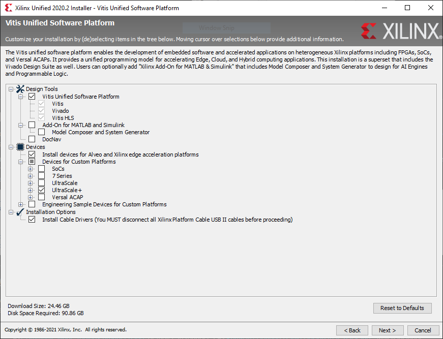
The main tool used for programming the FPGA is the Xilinx Software Commandline Tool is a tool included as part of the installation of the Xilinx Vitis platform. An example sequence of commands will resemble what is below. However, this will vary depending on the location of the files and programming will be performed later.
* Xilinx Software Commandline Tool (XSCT) v2019.1
  *** Build date : May 24 2019-15:06:52
    ** Copyright 1986-2018 Xilinx, Inc. All Rights Reserved.

xsct% cd Desktop/Quad_Mxfe_Files
xsct% source run.vcu118_quad_ad9081_204c_txmode_11_rxmode_4_revc.tcl
MATLAB (Optional)
MATLAB is used to exercise the board through LibIIO objects and provide higher level application functionality. See the High Speed Converter Toolbox documentation for supported MATLAB versions and supported boards.
In order to work with the platform, a number of toolboxes and support packages are required:
Communications Toolbox Support Package for Xilinx Zynq-Based Radio. Installed through MATLAB Add-On Explorer.
Analog Devices High Speed Converter Toolbox. Can be installed through MATLAB Add-On Explorer or latest version here: High Speed Converter Toolbox Download Page
Customers can request a free trial via the Communications Toolbox product page, or they can request a Software-Defined Radio Design trial package, which includes MATLAB, Simulink, DSP System Toolbox, Signal Processing Toolbox, and Communications Toolbox.
Example Quad-MxFE MATLAB scripts are provided: Example Quad-MxFE MATLAB Scripts
Quick start bringup with hardware
All the products described on this page include ESD (electrostatic discharge) sensitive devices. Electrostatic charges as high as 4000V readily accumulate on the human body or test equipment and can discharge without detection. Although the boards feature ESD protection circuitry, permanent damage may occur on devices subjected to high-energy electrostatic discharges. Therefore, proper ESD precautions are recommended to avoid performance degradation or loss of functionality. This includes removing static charge on external equipment, cables, or antennas before connecting to the device.
This section assumes the following:
Standoffs have been attached to Quad MxFE board
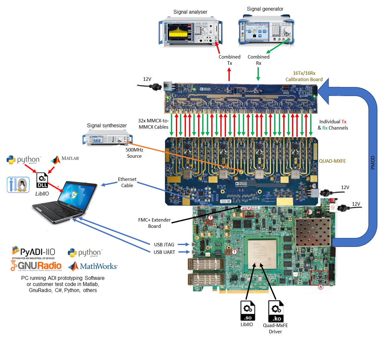
VCU118 and Quad MxFE have been attached via a FMC+ extender on the FMC+
Ethernet cable has been connected to VCU118 and connected to USB to Ethernet
USB to Ethernet dongle has IP address of 192.168.2.5. For locally connected FPGAs (i.e. Ethernet cable from VCU118 to USB to Ethernet dongle), the Hostname is
192.168.2.1. This assumes that the USB to Ethernet dongle has been configured with an IP address of192.168.2.xwherexrepresents a number 0 to 255 (excluding 1). This can be seen in the image. These settings are accessed (in Windows 10) by typing Network into the start menu then choose the “change adapter options” select and right click on the USB to Ethernet dongle. Select properties from the right click menu. Once the IP has been set, it will be remembered on the computer. Click ok on both windows to close and save the Dongle IP settings.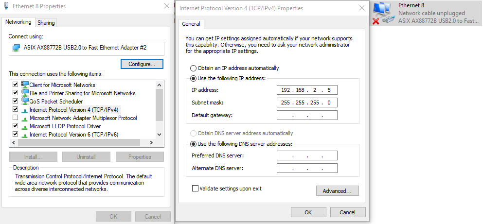
2x micro USB cables have been connected to PC and VCU118 for JTAG and Serial
All required software programs have been installed. See here for full list: Prerequisites
All FPGA images/script files have been built and placed in a folder on the Desktop called QuadMxFE
500MHz ~0dBm source has been attached to Quad MxFE central clock input SMA
12V power bricks (>8A for Quad MxFE and >5A for VCU118) have been connected to boards
Fans have been turned on
General board power up/programming sequence
The power up sequence is not difficult:
Power up the 500MHz oscillator
Power up the Quad MxFE Board
Power on the VCU118 board
Once these are powered up, program the FPGA:
Open Putty at the correct COM port and baudrate of 115200. See this section to determine the correct COM port Putty Configuration
Open Xilinx Command Line Tool (XSCT). Open it from the Start Menu under Xilinx –> Xilinx Software Commandline Tool. Once the prompt is open, type:
cd Desktop\QuadMxFEIf the files were unzipped somewhere else, then change directory to that folder.Run the loading script for the particular build by typing the following (example) in XSCT:
source
run.vcu118_quad_ad9081_204c_txmode_11_rxmode_4_revc.tcl
The statement above will launch the programming of the first build, but the others can be run by changing the name of the particular .tcl file to be loadedWait for the programming to finish in XSCT. This should show that the tcfchan#1 was closed as the final step.
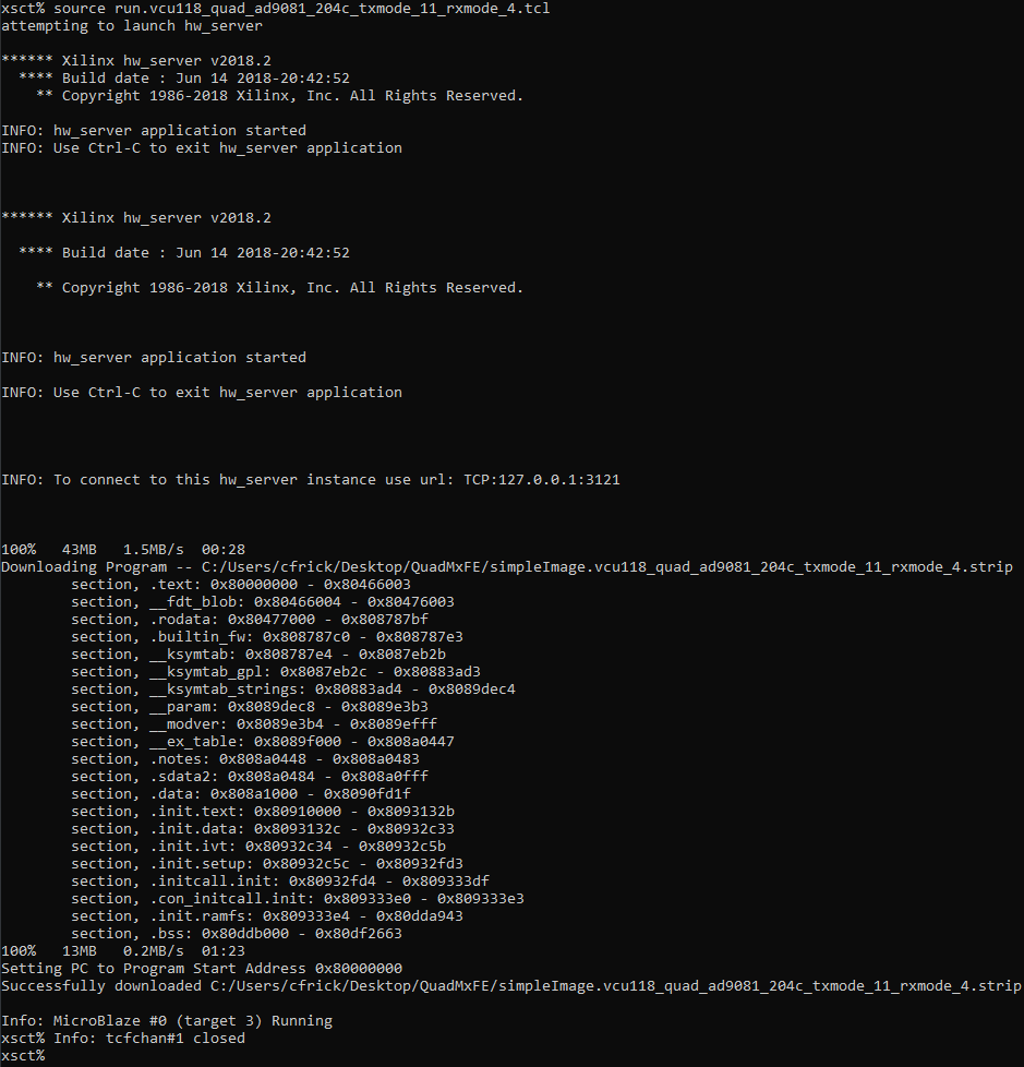
Wait for the build to boot completely by checking the Putty terminal window. The putty window shows the progress of the Linux image booting. Wait for the login prompt as shown at the bottom.
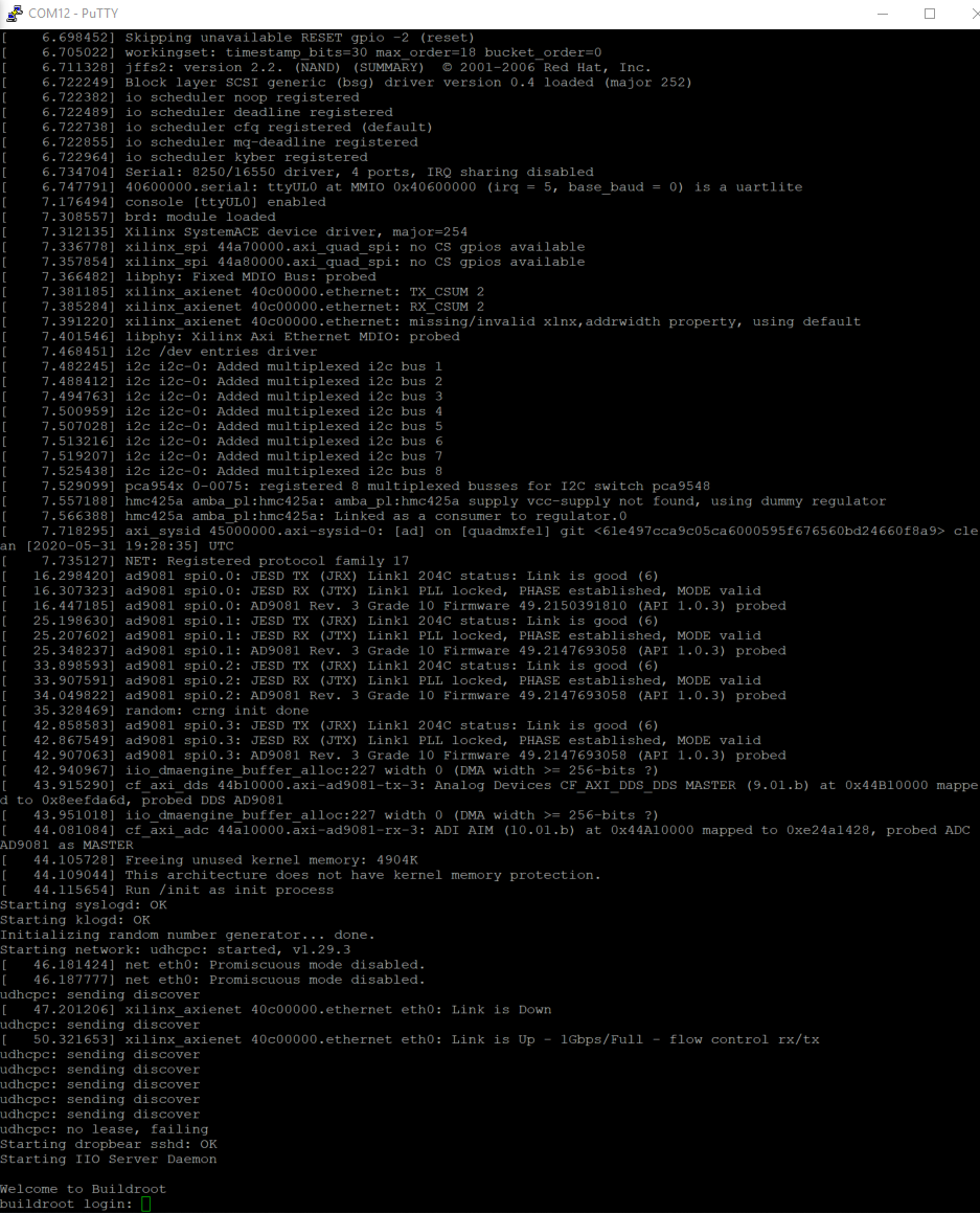
This example output is from the Txmode 11 Rxmode 4 image output. At this point, the image is ready to use in MATLAB or additional debug steps can be performed. To log into the image, the username and password are
UN: root
PW: analog
At this point the FPGA has booted and all of the blue PLL lights should be illuminated. The FPGA is ready to be controlled from MATLAB or from IIO Oscilloscope.
To work in IIO Oscilloscope, open IIO Oscilloscope and use the GUI
To control through MATLAB, Please refer to the following section. There are a number of example scripts that highlight various aspects of the Quad MxFE.
MATLAB control overview
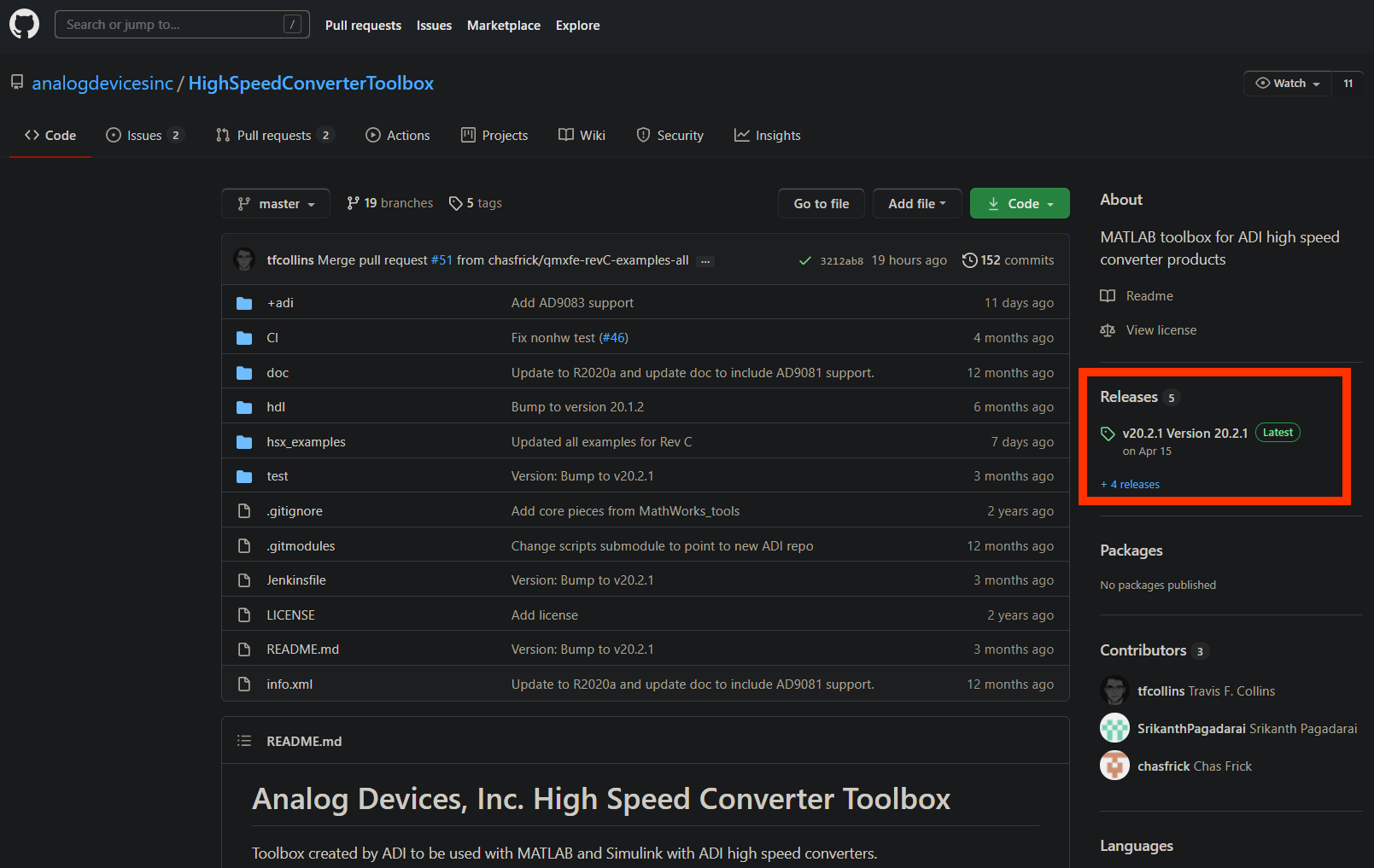
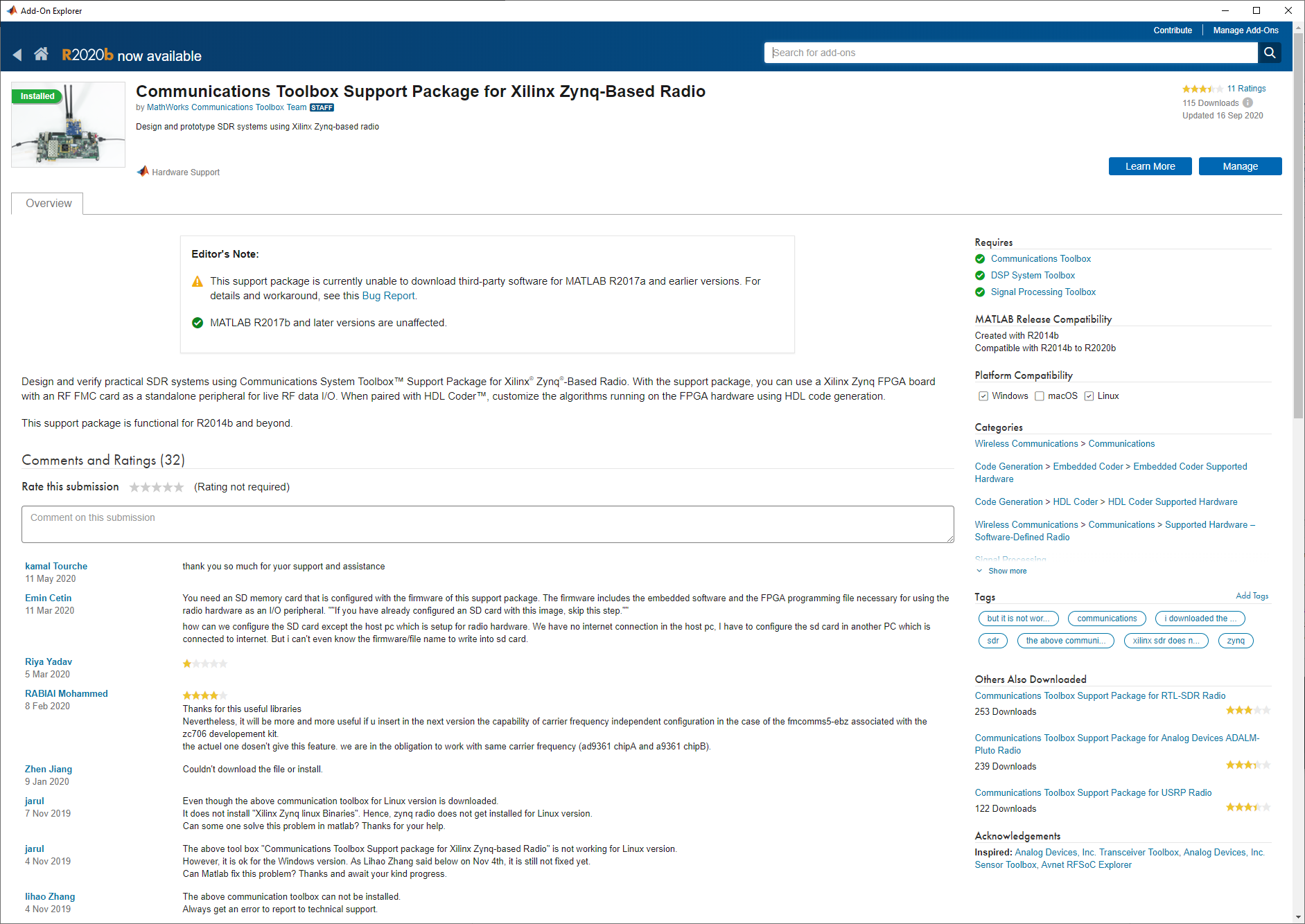
The Quad-MxFE Platform can be controlled via MATLAB using example scripts which are available as part of the Analog Devices, Inc. High Speed Converter Toolbox add-on. This add-on can either be manually downloaded from the Releases section of the GitHub page or downloaded and installed via MATLAB Add-On Explorer. NOTE: it’s recommended to install via the download from GitHub as this is generally more up to date than the MATLAB Add-On Explorer page Please ensure you have installed both the Analog Devices, Inc. High Speed Converter Toolbox as well as the Communications Toolbox Support Package for Xilinx Zynq-Based Radio as shown below (Zynq-Based Radio Toolbox).
Example scripts are located within the add-on install directory, which is
usually located in the C:\Users\<username>\AppData\Roaming\MathWorks\MATLAB
Add-Ons\Toolboxes directory. The example scripts are specifically located in
the following folder: Analog Devices, Inc. High-Speed Converter
Toolbox\hsx_examples\qmxfe
Controlling Quad-MxFE with MATLAB
The control interface for the Quad-MxFE is implemented using standard system objects in MATLAB. Basic information for instantiating the objects is provided in the toolbox documentation within MATLAB and on this page. Here is an example instantiation of the objects:
>> tx = adi.QuadMxFE.Tx()

tx =

  adi.QuadMxFE.Tx with properties:

    ChannelNCOFrequenciesChipA: [0 0 0 0 0 0 0 0]
    ChannelNCOFrequenciesChipB: [0 0 0 0 0 0 0 0]
    ChannelNCOFrequenciesChipC: [0 0 0 0 0 0 0 0]
    ChannelNCOFrequenciesChipD: [0 0 0 0 0 0 0 0]
       MainNCOFrequenciesChipA: [0 0 0 0]
       MainNCOFrequenciesChipB: [0 0 0 0]
       MainNCOFrequenciesChipC: [0 0 0 0]
       MainNCOFrequenciesChipD: [0 0 0 0]
         ChannelNCOPhasesChipA: [0 0 0 0 0 0 0 0]
         ChannelNCOPhasesChipB: [0 0 0 0 0 0 0 0]
         ChannelNCOPhasesChipC: [0 0 0 0 0 0 0 0]
         ChannelNCOPhasesChipD: [0 0 0 0 0 0 0 0]
            MainNCOPhasesChipA: [0 0 0 0]
            MainNCOPhasesChipB: [0 0 0 0]
            MainNCOPhasesChipC: [0 0 0 0]
            MainNCOPhasesChipD: [0 0 0 0]
     ChannelNCOGainScalesChipA: [0 0 0 0 0 0 0 0]
     ChannelNCOGainScalesChipB: [0 0 0 0 0 0 0 0]
     ChannelNCOGainScalesChipC: [0 0 0 0 0 0 0 0]
     ChannelNCOGainScalesChipD: [0 0 0 0 0 0 0 0]
               NCOEnablesChipA: [0 0 0 0 0 0 0 0]
               NCOEnablesChipB: [0 0 0 0 0 0 0 0]
               NCOEnablesChipC: [0 0 0 0 0 0 0 0]
               NCOEnablesChipD: [0 0 0 0 0 0 0 0]
         EnableResampleFilters: 0
      CalibrationBoardAttached: false
                           uri: 'ip:analog'
               EnabledChannels: 1
                    DataSource: 'DMA'
           EnableCyclicBuffers: false

>> rx = adi.QuadMxFE.Rx()

rx =

  adi.QuadMxFE.Rx with properties:

    ChannelNCOFrequenciesChipA: [0 0 0 0]
    ChannelNCOFrequenciesChipB: [0 0 0 0]
    ChannelNCOFrequenciesChipC: [0 0 0 0]
    ChannelNCOFrequenciesChipD: [0 0 0 0]
       MainNCOFrequenciesChipA: [0 0 0 0]
       MainNCOFrequenciesChipB: [0 0 0 0]
       MainNCOFrequenciesChipC: [0 0 0 0]
       MainNCOFrequenciesChipD: [0 0 0 0]
         ChannelNCOPhasesChipA: [0 0 0 0]
         ChannelNCOPhasesChipB: [0 0 0 0]
         ChannelNCOPhasesChipC: [0 0 0 0]
         ChannelNCOPhasesChipD: [0 0 0 0]
            MainNCOPhasesChipA: [0 0 0 0]
            MainNCOPhasesChipB: [0 0 0 0]
            MainNCOPhasesChipC: [0 0 0 0]
            MainNCOPhasesChipD: [0 0 0 0]
                 TestModeChipA: 'off'
                 TestModeChipB: 'off'
                 TestModeChipC: 'off'
                 TestModeChipD: 'off'
              EnablePFIRsChipA: false
              EnablePFIRsChipB: false
              EnablePFIRsChipC: false
              EnablePFIRsChipD: false
            PFIRFilenamesChipA: ''
            PFIRFilenamesChipB: ''
            PFIRFilenamesChipC: ''
            PFIRFilenamesChipD: ''
           ExternalAttenuation: 0
               SamplesPerFrame: 32768
         EnableResampleFilters: 0
      CalibrationBoardAttached: false
                           uri: 'ip:analog'
               EnabledChannels: 1
CalBoardVCU118.m
This folder also contains a driver file CalBoardVCU118.m for controlling the
optional 16 Tx / 16 Rx Calibration Board via the
VCU118 PMOD interface intended to mate to the Quad-MxFE Platform. This driver
file allows the user to perform the following functions after instantiation
using CalibrationBoard = CalBoardVCU118:
CalibrationBoard.ConfigureCombinedLoopback: Loop Combined Tx Channels Back Into Combined Rx PathCalibrationBoard.ConfigureAdjacentIndividualLoopback: Loop Individual Tx Channels Back Into Adjacent Rx PathCalibrationBoard.ConfigureTxOutSMA: Send Combined Tx Channels OutJ502SMA Connector For Off-Board AnalysisCalibrationBoard.ConfigureRxInFromSMA: Send Combined Rx Input IntoJ501SMA Connector & Inject Into All Rx ChannelsCalibrationBoard.ConfigureTxOutToLTC5596: Send Combined Tx Channel Signal Into LTC5596 Power DetectorCalibrationBoard.QueryAD8318_voltage: Poll the Measured AD8318 Power Detector Voltage From the On-Board AD5592R ADCCalibrationBoard.QueryHMC948_voltage: Poll the Measured HMC948 Power Detector Voltage From the On-Board AD5592R ADCCalibrationBoard.QueryLTC5596_voltage: Poll the Measured LTC5596 Power Detector Voltage From the On-Board AD5592R ADC
If the user intends to use the 16 Tx / 16 Rx Calibration Board in their
analysis, then be sure to enable tx.CalibrationBoardAttached = 1 and
rx.CalibrationBoardAttached = 1 in the tx and rx channel initialization.
LoadVcu118Code.m
For convenience, there is also a function file available named
LoadVcu118Code.m which allows the user to load new .tcl files via the MATLAB
interface that correspond to the available use cases presently supported with
the Quad-MxFE Platform. These .tcl files can be obtained from the .zip file
download available on the
Quad-MxFE Software Quick Start Guide.
The default configuration for the example scripts is such that the code is
commented for this function, but the user can uncomment it at the beginning of
loading the new bitstream, then execute the function and re-comment it so that
the system doesn’t boot each time the script is run. Be sure to wait until the
system fully boots prior to executing any additional MATLAB scripting. The boot
process can take a few minutes and status can be obtained via a terminal window
such as PuTTY. Please install the Vivado Toolchain in order to know the path for the Xilinx Software
Command Line Tool (XSCT) to be able to utilize this feature.
LoadVcu118Code(xsctpath,tclpath): First parameter: Installed xsct.bat folder; 2nd Parameter: Downloaded .\run.tcl’ file location
Presently there are three MATLAB example scripts. The default uri for the
connection to the VCU118 is 192.168.2.1. Please ensure that no VPN
connection is present when trying to establish a connection to the Quad-MxFE
Platform.
These three scripts perform the following applications:
QuadMxFE_SimpleTxRx.m
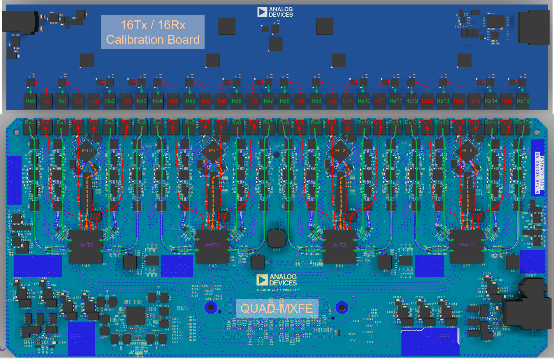
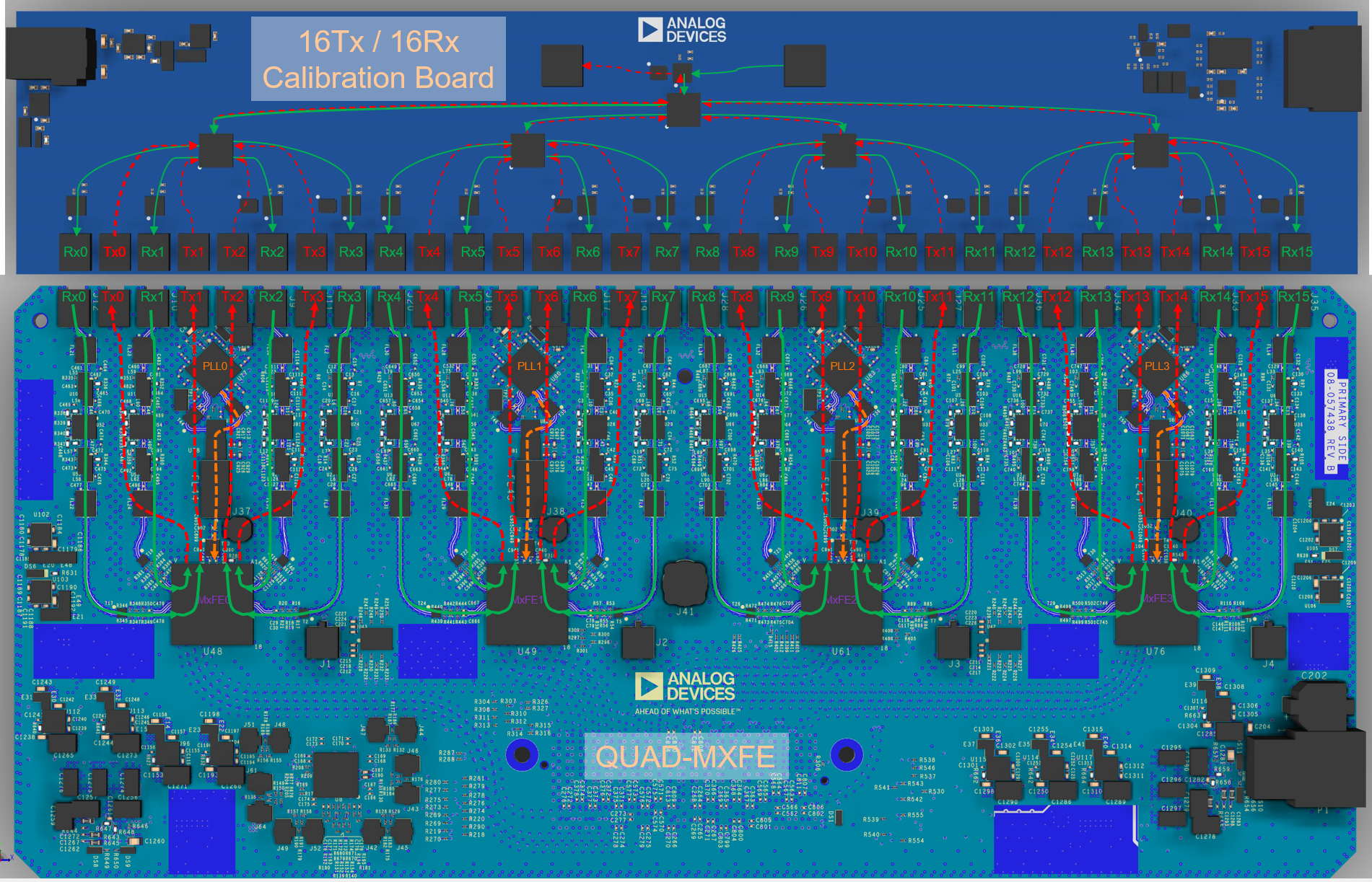
The default test setup for this script uses the 16Tx/16Rx Calibration Board as shown below in which each Tx channel is looped back into the adjacent Rx channel after going through a 10dB attenuator on the 16Tx/16Rx Calibration Board.
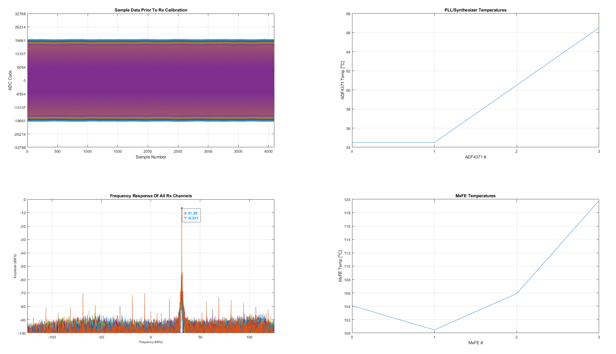
This script is to be used with the Analog Devices Quad-MxFE Platform to
demonstrate relatively simple MATLAB control of the system. It allows the user
to configure the Tx and Rx aspects of the system by using the tx =
adi.QuadMxFE.Tx and rx = adi.QuadMxFE.Rx system objects. The script then
loads transmit waveforms and captures receive data for all channels on the
system. All enabled Rx channels are then plotted in both the time domain and the
frequency domain as an overlay plot. The script also polls the measured
temperatures of the four ADF4371 and four AD9081 in the system and
then plots those temperatures. No Rx nor Tx calibration is performed, nor are
any multi-chip synchronization algorithms. The default configuration for this
script uses the 16 Tx / 16 Rx Calibration Board in adjacent individual loopback
mode. If the user does not have this part of the platform they will need to
ensure they modify the script accordingly.
Using this script as a basis, the user can modify the script for their own use case such that they can:
Inject Custom Tx Waveforms for Each Enabled Tx Channel Using
tx(waveformDataMatrix)Change Tx NCO Frequencies Using, For Example,
tx.MainNCOFrequenciesChipAortx.ChannelNCOFrequenciesChipAChange Tx NCO Phases Using, For Example,
tx.MainNCOPhasesChipAortx.ChannelNCOPhasesChipACapture Simultaneous Complex-Valued Rx Data for All Enabled Channels:
rxData=rx()Change Rx NCO Frequencies Using, For Example,
rx.MainNCOFrequenciesChipAorrx.ChannelNCOFrequenciesChipAChange Rx NCO Phases Using, For Example,
rx.MainNCOPhasesChipAorrx.ChannelNCOPhasesChipAChange On-Board Digital Step Attenuator Value Located in the Rx Front-Ends Using
rx.ExternalAttenuationChange 16Tx/16Rx Calibration Board Configuration
Perform MxFE Register Reads/Writes
Analyze and Post-Process Captured Waveforms
More information can be found on the Tx and Rx system objects by typing within
the MATLAB Command Window help adi.QuadMxFE.Tx and/or help
adi.QuadMxFE.Rx and then selecting the ‘Documentation for adi.QuadMxFE.Tx’
hyperlink. NCO frequencies/phases can be changed real-time using the respective
Tx or Rx system object. If, at any point, the user tries to load a different
buffer size into the Tx waveforms they will need to first release(tx) and
then call tx once more. Likewise, if a different sized data capture is
needed, then first issue a release(rx) before changing
rx.SamplesPerFrame. Note that users with their own waveform should inject
their own waveform data within the tx() call instead of using the sine array as
in the example script.
QuadMxFE_SystemAlignmentFIR.m
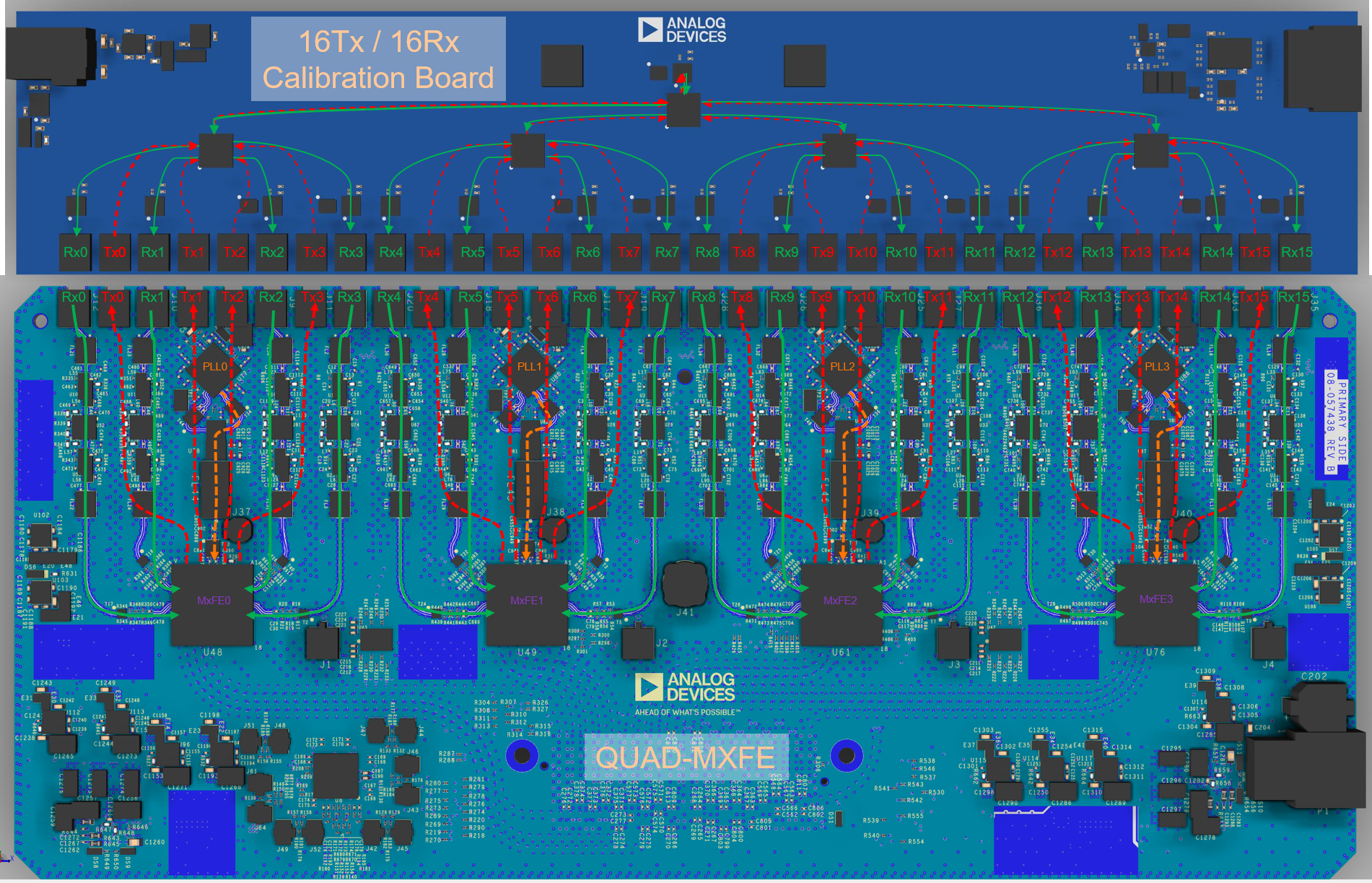
The default test setup for this script uses the 16Tx/16Rx Calibration Board as shown below in which each Tx channel is combined and then looped back into the combined Rx path after going through a 2dB attenuator on the 16Tx/16Rx Calibration Board. The combined Rx signal is then split into each Rx channel.
Important
Once the pFIRs have been enabled through this script, they will remain on and will cause problems if other non pFIR scripts are run. Therefore a complete platform reboot is required between running the pFIR script followed by any other MATLAB script
This script is to be used with the Analog Devices Quad-MxFE Platform to demonstrate MATLAB control of the programmable finite impulse response (pFIR) filters and NCO phase offsets in order to phase align all Rx and Tx channels in the system. It allows the user to configure the Tx and Rx aspects of the system and then load transmit waveforms and capture receive data for all channels on the system. The script uses the on-system DSP blocks to phase-align the ADF4371 device clocks by a PLL Synthesizer Phase Adjustment Process. After this, it phase-aligns all Tx channels and then loads a broadband chirp waveform into each Tx channel which spans the frequency range of the Tx I/Q data rate. It ends by also phase- and amplitude-aligning all Rx RF channels using the NCO phase offsets and pFIRs assigned to each Rx channel. It shows the process by which a calculated error response (with respect to Rx0 as the baseline) can be used to generate a 96-tap real pFIR design and then how to quantize and load that pFIR design into the system. Finally, it plots the results to determine the phase and amplitude alignment accuracy. It provides an example of how to use pFIRs with the system to obtain Rx channel equalization and gain flatness.
The output of this script are a few pFIR configuration files with a filename,
for example QuadMxFE_DualReal_CH0and1_3.2GHz.cfg, for all the Rx channels.
Additionally, many figures are plotted to aid with system analysis:
Figure 1: The Tx phase-alignment results are shown using the pulsed baseband waveform in which only one Tx channel is output at a time but still uses the same Tx waveform matrix. After combining all the Tx channels however using the 16Tx/16Rx Calibration Board, and then injecting this signal into the first Rx channel of each MxFE (Rx0, Rx4, Rx8, and Rx12), the ADF4371 phases are adjusted to ensure that the pulse phases of Tx0, Tx4, Tx8, and Tx12 are aligned. The top plots show the time response of received pulse trains, whereas the bottom plots show the cross-correlation of these signals with respect to Rx0.
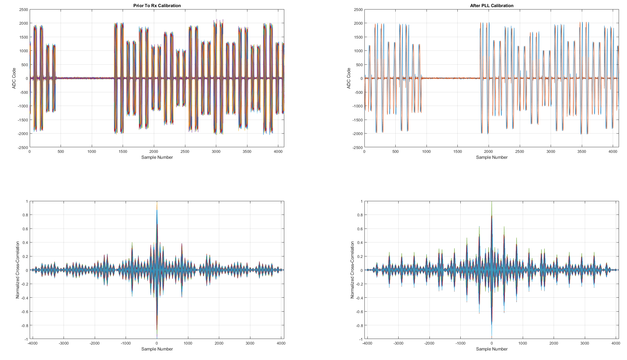
Figure 2: The Tx phases of the pulsed waveform used to determine Tx alignment is shown. A common receiver (Rx0) detects a pulse train with the number of pulses equal to the number of enabled Tx channels in the system. The phase of each pulse directly relates to the phase of the Tx channel. The bottom plot shows the phase alignment of all Tx pulses, which therefore correspond to phase-alignment of all Tx channels.
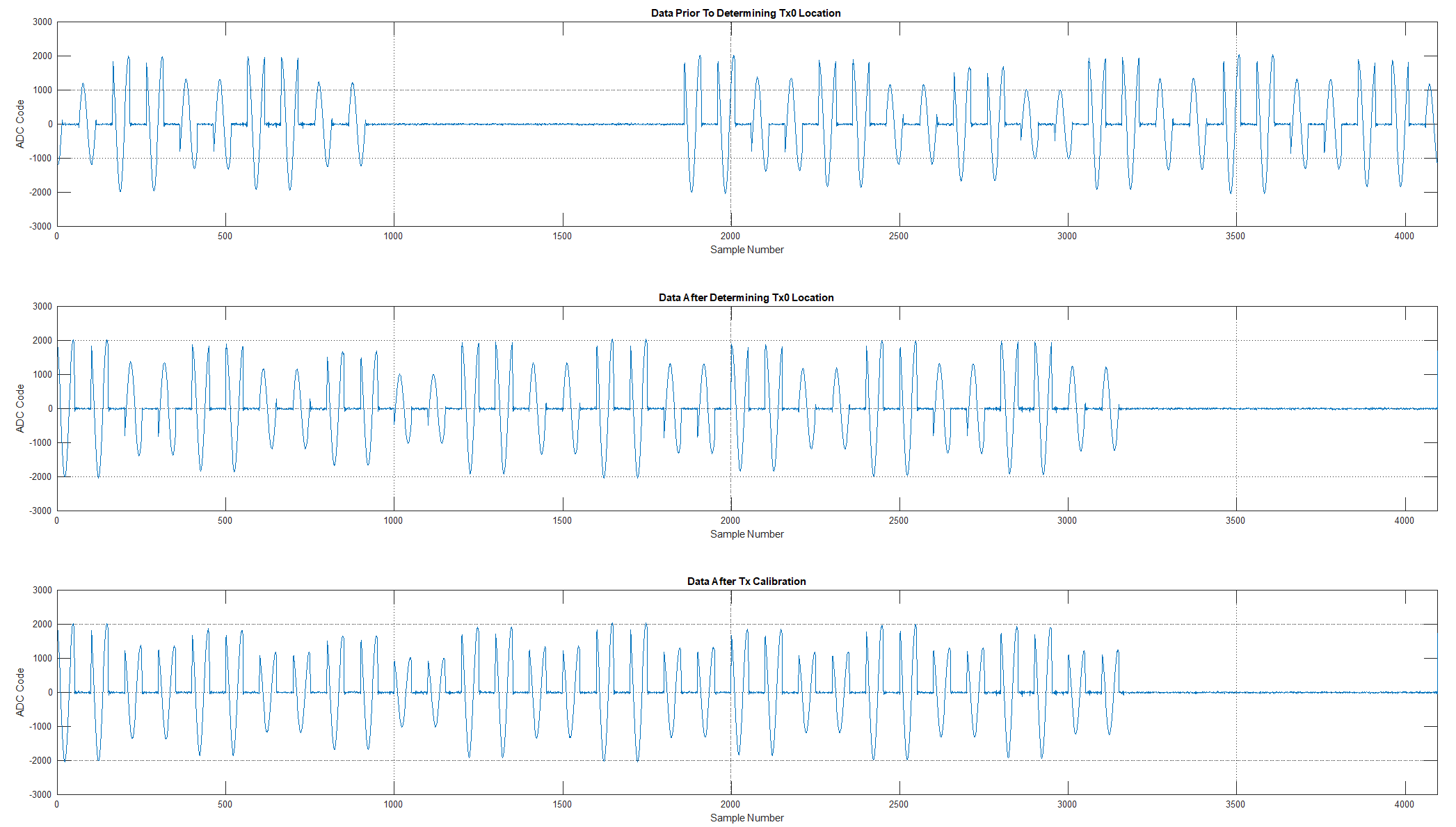
Figure 3: Shows the time domain ADC capture, corresponding chirp FFT, and amplitude and phase errors for each channel with respect to Rx0 both before and after Rx calibration.
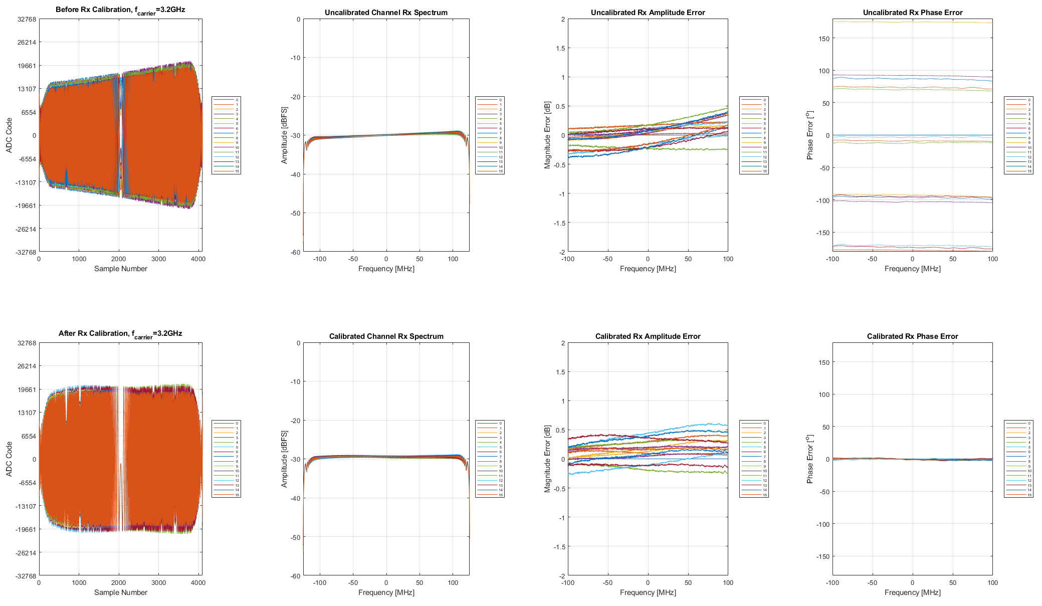
Figure 4: Shows the calculated error response of each Rx channel in terms of its phase and amplitude error prior to Rx calibration.
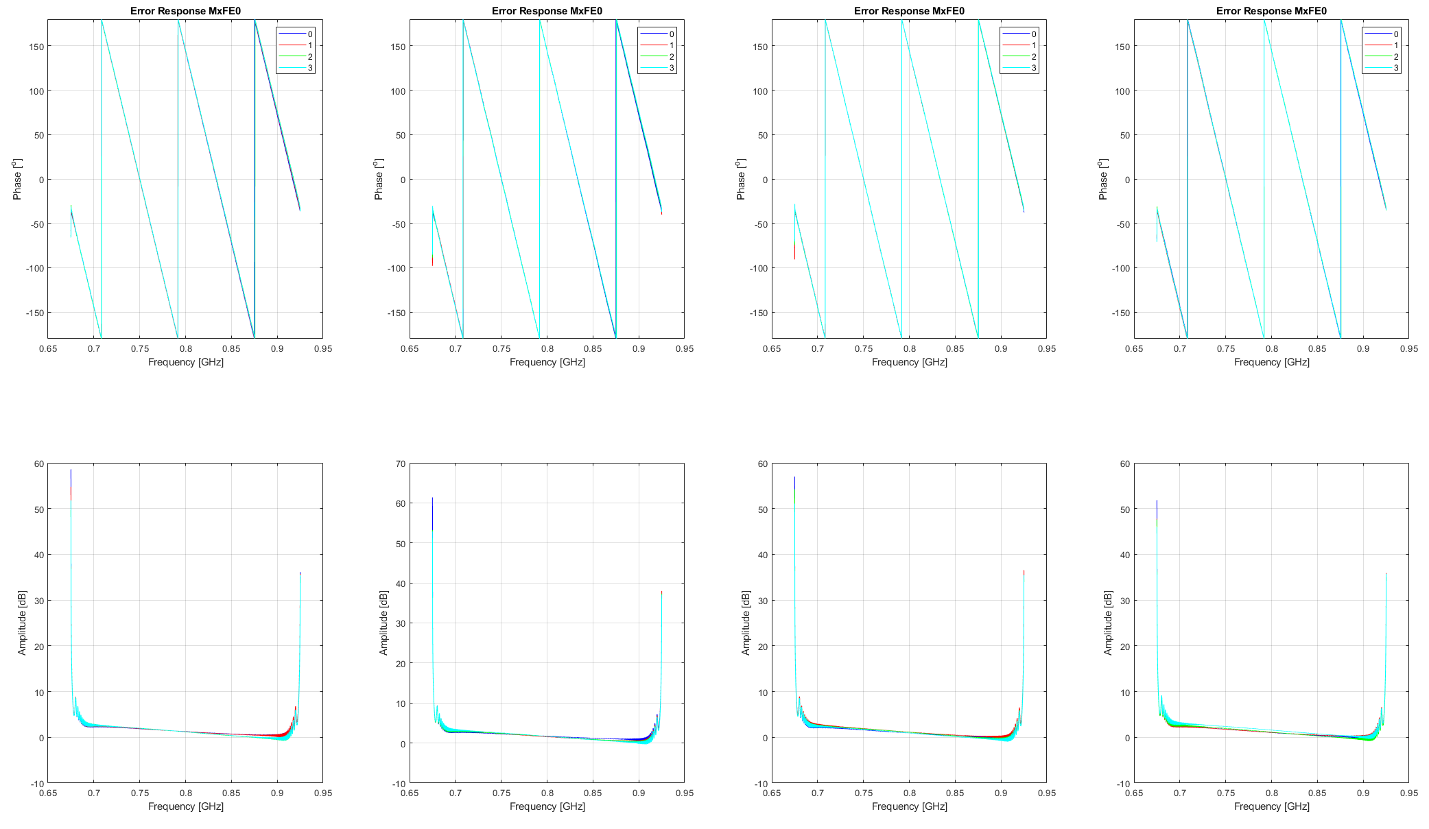
Figure 5: Presents the magnitude and phase response of the designed pFIRs based on that calculated error response.
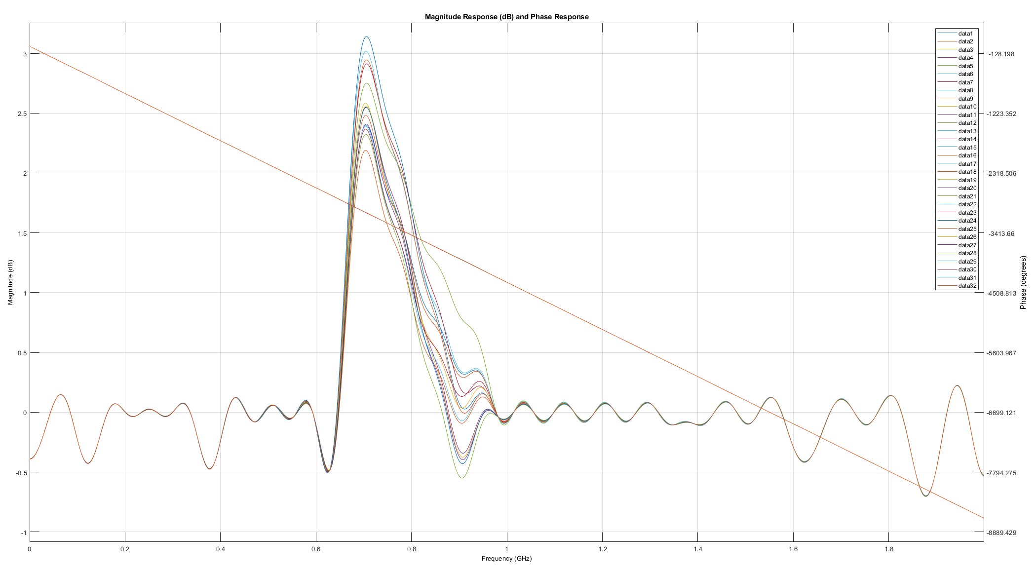
Figure 6: Shows the individual pFIR tap coefficients both before and after quantization for each Rx channel.
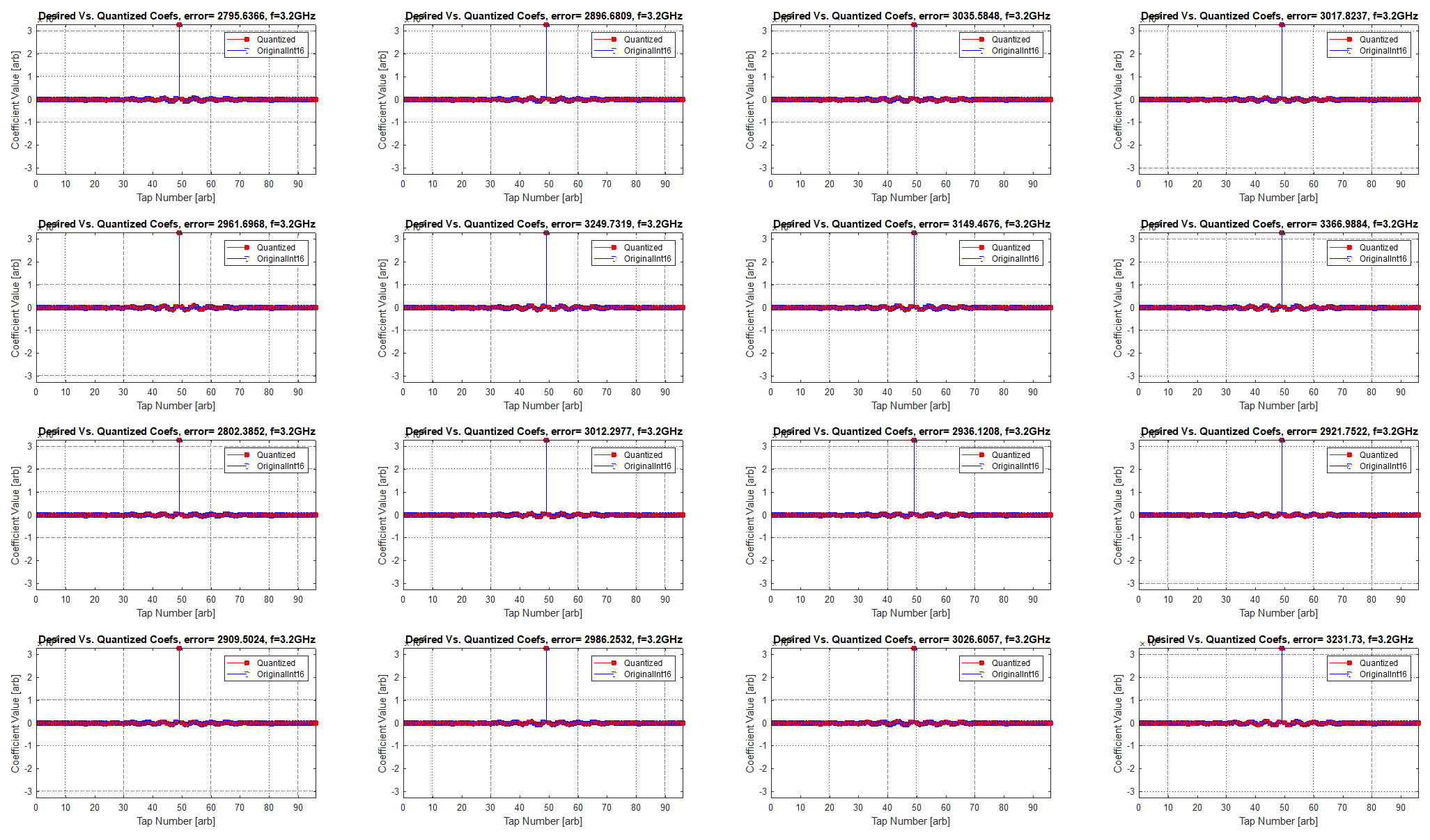
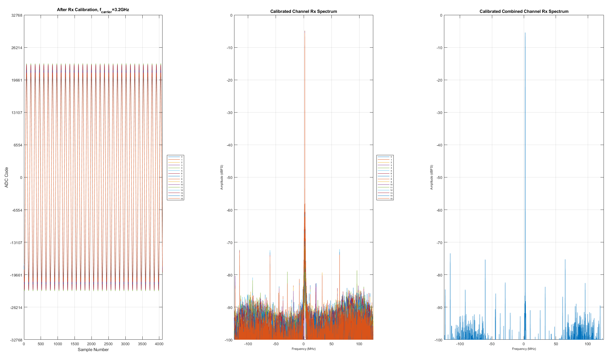
Figure 7: Shows the combined Rx system performance using a single-tone waveform after all Rx channels are phase- and amplitude-aligned.
QuadMxFE_MCS.m
This script is to be used with the Analog Devices Quad-MxFE Platform to demonstrate MATLAB control of the system. It allows the user to configure the Tx and Rx aspects of the system and then load transmit waveforms and capture receive data for all channels on the system. The script uses the on-system DSP blocks to align the device clocks and output/input RF channels using the NCO phase offsets. Finally, it plots the results of a multi-chip synchronization (MCS) algorithm and allows the user to save a .mat file containing the run results.
This .mat file, if saved to the
.\Baseline Files Using ADF4371 Phase Adjustment\Align Using Tx\
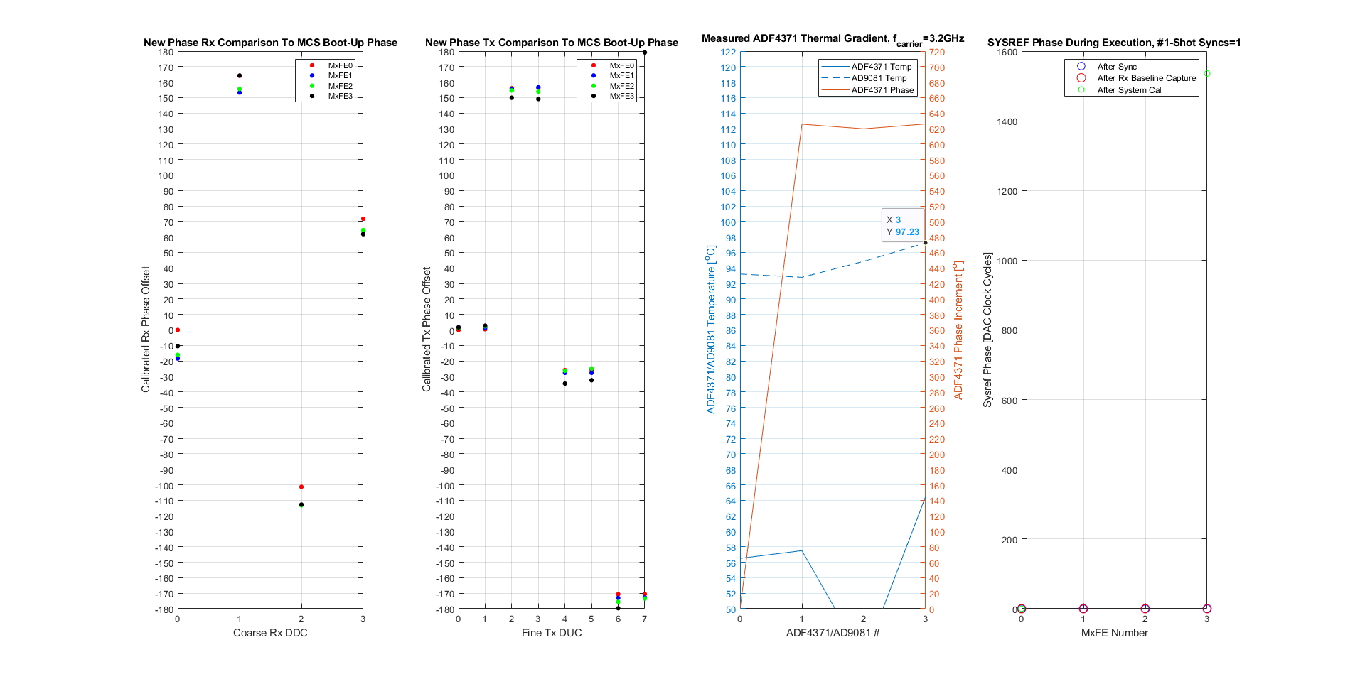
directory after the first time the script is run, can be used as a baseline power-up synchronization comparison to subsequent script executions. In this way, the user can determine the performance of the MCS features on the platform and view the deterministic phase relationship of the NCO phase offsets for a given NCO frequency. The open circles are grabbed from the baseline in the directory shown above, whereas the solid dots are the new NCO phase offsets after a subsequent power cycle or script execution.
The test setup is the same as that used for the QuadMxFE_SystemAlignmentFIR.m script. More information on MCS can be found in the Multi-Chip Synchronization with the Quad-MxFE + Calibration Board User Guide.
The output of this script includes a .mat file containing the script execution results with a filename dependent on the system configuration and date of execution; for example 3.2GHz_AlignADF4371s_1_AlignPLLRxs_0_1.9531MHzOffset_14_56_24__11_11_2020.mat. Additionally, many figures are plotted to aid with system analysis:
Figure 1: The ADF4371 PLL/synthesizer calibration results are shown on the top-left two plots, showing the alignment of each zeroth Tx channel on each MxFE in the platform. The two right plots show the time domain data capture after injecting a CW tone into each Tx channel, the corresponding normalized cross-correlation for each Rx channel after calibration, the FFT of that time domain capture, and the combined 16-channel FFT showing the improved noise floor performance.
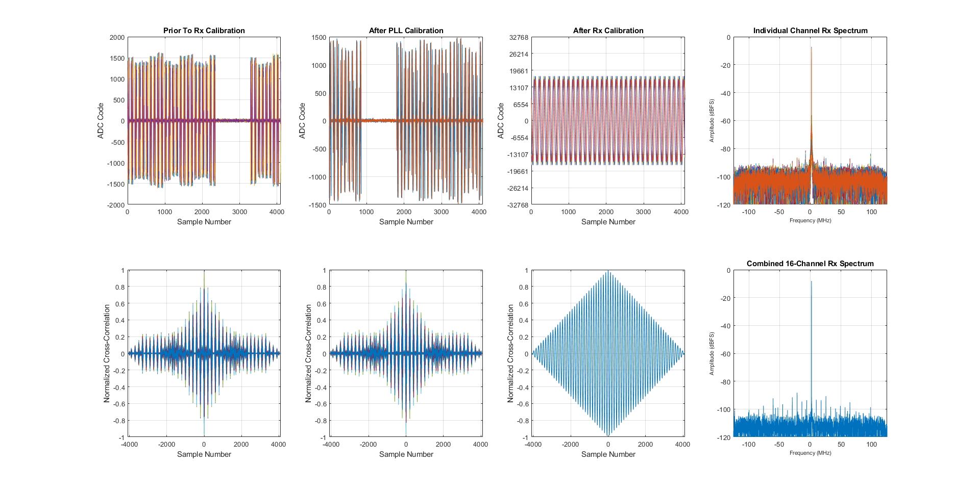
Figure 2: The Tx phase-alignment results are shown using the pulsed baseband waveform in which only one Tx channel is output at a time but still uses the same Tx waveform matrix. After combining all the Tx channels however using the 16Tx/16Rx Calibration Board, and then injecting this signal into the first Rx channel of each MxFE (Rx0, Rx4, Rx8, and Rx12), the ADF4371 phases are adjusted to ensure that the pulse phases of Tx0, Tx4, Tx8, and Tx12 are aligned. The top plots show the time response of received pulse trains, whereas the bottom plots show the cross-correlation of these signals with respect to Rx0.
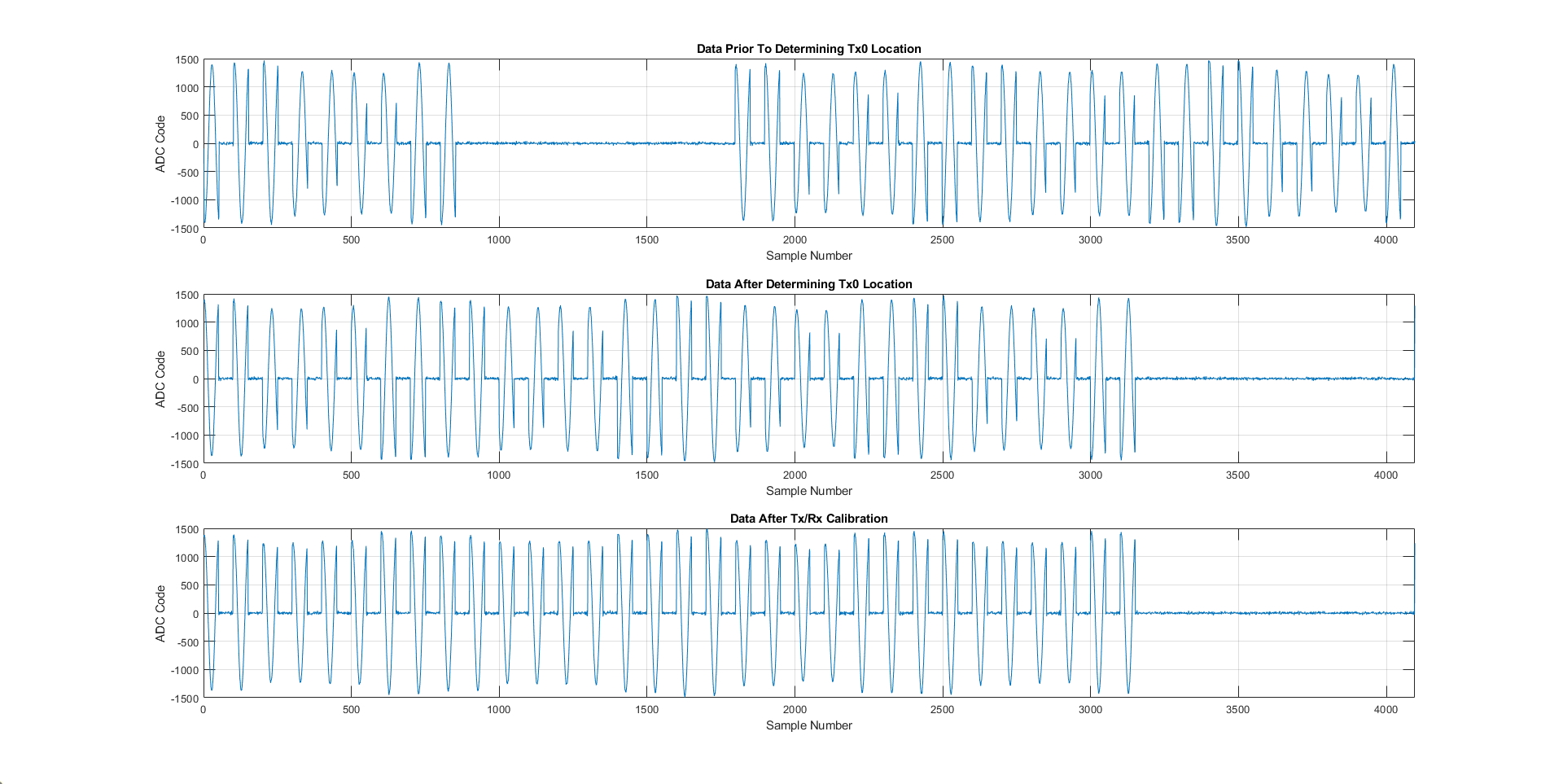
Figure 3: If attached, Figure 3 shows the 16Tx/16Rx Calibration Board’s adjacent loopback performance.
Figure 4: A full I/Q band chirp signal is injected into each Tx channel and a corresponding data capture is performed. Then a single-frequency CW signal is injected into each Tx channel and a corresponding data capture is performed. The left side of the figure shows the individual time domain and frequency domain results, as well as the combined Rx performance. The right side shows similar results for the single-frequency CW signal.
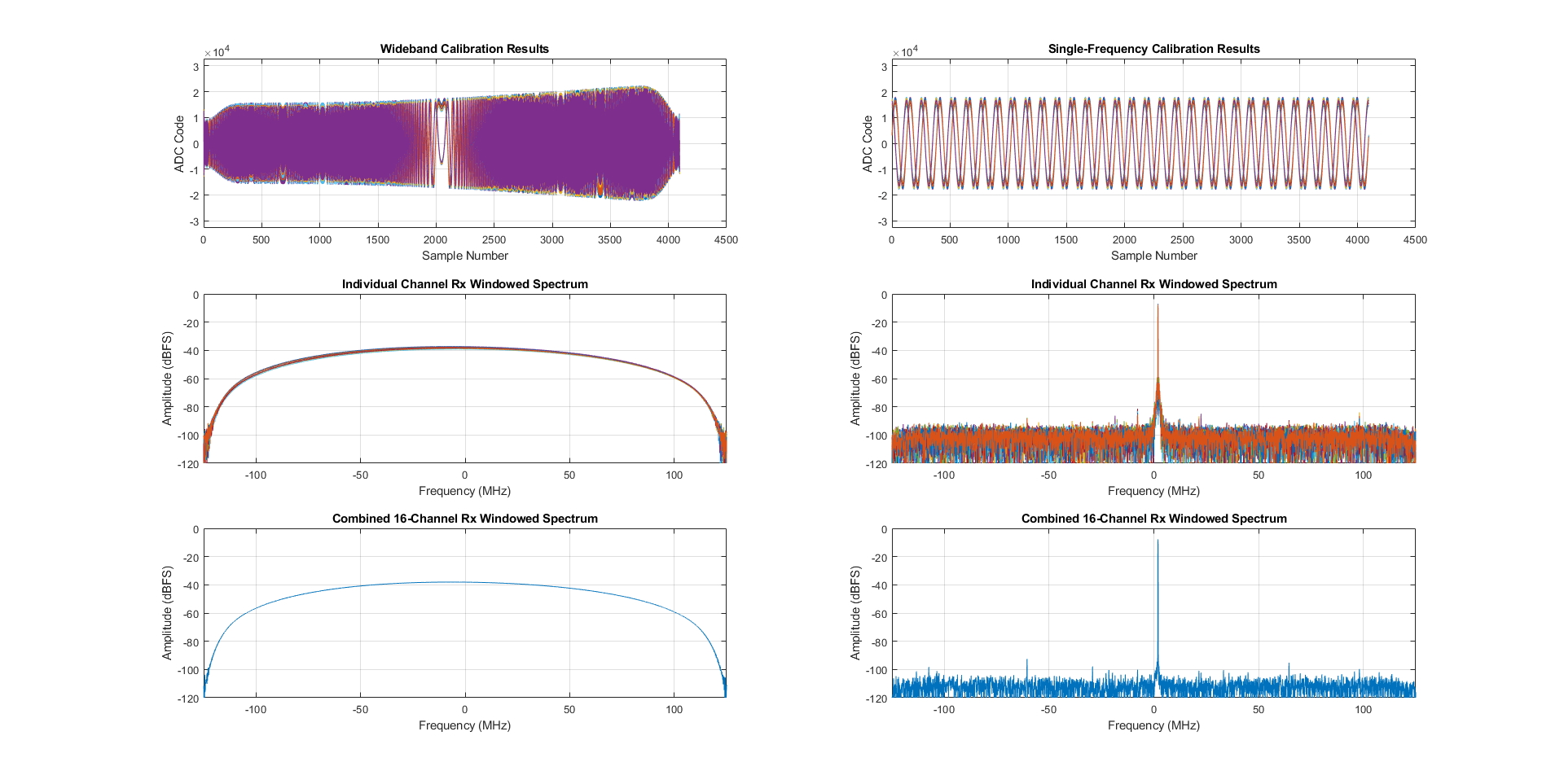
Figure 5: The MCS results from running the script are shown. The left-most plot shows the comparison between the new (solid dots) and baseline (open circles) Rx NCO phase offsets. The second-from-the-left plot shows the comparison between the new (solid dots) and baseline (open circles) Tx NCO phase offsets. If MCS is functioning as expected the solid dots should be inside the open circles. The second-from-the-right plot shows the phase adjustment applied to each ADF4371 PLL/synthesizer IC on the system and the corresponding thermal gradients measured for each MxFE and PLL chip. The right-most plot shows the SYSREF phase stability at different portions of the script’s execution.
QuadMxFE_ADCtoDAC_Loopback.m
The Quad-MxFE Platform is capable of configuring each ad9081 into a mode such that the digitized ADC output can be sent through the DDCs and looped back on-chip into the DUCs prior to being synthesized by the DACs. This allows the user to bypass the JESD204c digital interface and therefore achieve a low-latency loopback capability.
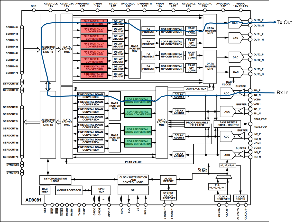
The default test setup for this script is shown below. This MATLAB script
provides an example of this for all MxFEs in the system. If the user injects a
combined Rx signal into J501 of the 16Tx/16Rx Calibration Board and connects
the combined Tx output to J502 of the Calibration Board to a spectrum
analyzer, then after running this script the user can then change the input
frequency and/or amplitude to observe the repeating or frequency translating
functions.
Debug
No blue lights are visible on board
If no blue lights are visible on the board, then the PLLs are not locked. The most likely cause of this is the lack of a 500MHz source into J41. Check the input power and state of the source. It should be 500MHz @ ~0dBm. Once the 500MHz signal is verified, the FPGA programming must be rerun.