EVAL-ADICUP3029 Base Board
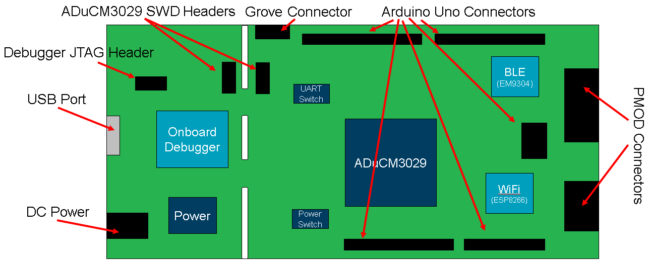
The EVAL-ADICUP3029 base board consists of two basic blocks:
An ultra low power, 32-bit ARM Cortex™-M3 processor, on a single chip ADuCM3029 microcontroller.
An on-board serial wire download (SWD) interface, which is implemented with the Freescale’s MК20DX128 microcontroller. This block allows the Freescale device to act as an on board debugger, so you don’t need additional external hardware to program or debug your ADuCM3029 applications.
This page describes the hardware peripheral connectors, jumpers and UART switch configurations options, , power configurations, connectivity options, the USB connectors and programming connections, and links to download the schematics and the layout.
Unboxing the EVAL-ADICUP3029
Peripheral Connectors
The following standard connectors are provided on the base board for customer to use with external add on modules:
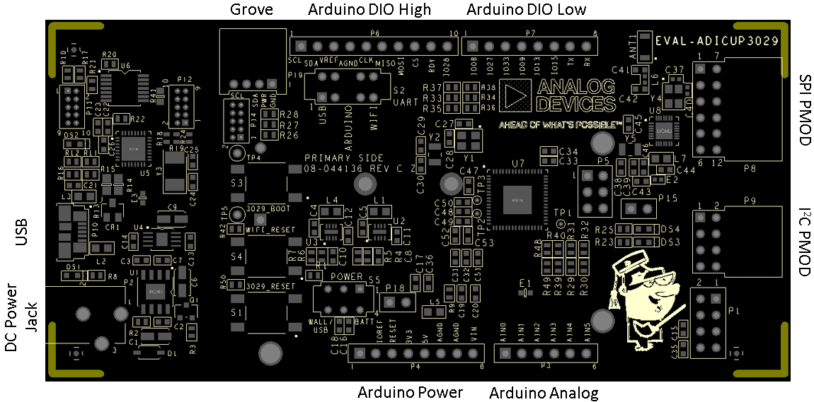
* DC Power Jack: Core positive, accepts +7V to +12V DC supply voltage.
* USB: Used for flash programming and debug interface; also can provide a virtual serial port connection to ADuCM3029 microcontroller.
* PMOD_SPI: 12-pin SPI PMOD connector.
* PMOD_I2C: 8-pin I2C PMOD connector.
Grove Connector: 4-pin I2C Grove connector.
* Arduino Connectors: Arduino Uno Rev3 compatible connectors.
All connector pin outs for the EVAL-ADICUP3029 are described in the table below.
Connector |
Pin No. |
Pin Name |
ADuCM3029 Pin Function |
ADuCM3029 Port No. |
|---|---|---|---|---|
Arduino DIO High |
1 |
SCL |
I2C0_SCL/GPIO04 |
P0_04 |
2 |
SDA |
I2C0_SDA/GPIO05 |
P0_05 |
|
3 |
AREF |
VREF+ |
||
4 |
AGND |
AGND (Analog ground) |
||
5 |
SCLK |
SPI0_CLK/SPT0_BCLK/GPIO00 |
P0_00 |
|
6 |
MISO |
SPI0_MISO/SPT0_BD0/GPIO02 |
P0_02 |
|
7 |
MOSI |
SPI0_MOSI/SPT0_BFS/GPIO01 |
P0_01 |
|
8 |
CS |
SPI0_CS1/SYS_CLKIN/SPI1_CS3/GPIO26 |
P1_10 |
|
9 |
RDY |
SPI0_RDY/GPIO30 |
P1_14 |
|
10 |
IO28 |
GPIO28 |
P1_12 |
|
Arduino DIO Low |
1 |
IO08 |
BPR0_TONE_N/GPIO08 |
P0_08 |
2 |
IO27 |
TMR1_OUT/GPIO27 |
P1_11 |
|
3 |
IO33 |
XINT0_WAKE3/TMR2_OUT/GPIO33 |
P2_01 |
|
4 |
IO09 |
BPR0_TONE_P/SPI2_CS1/GPIO09 |
P0_09 |
|
5 |
IO13 |
XINT0_WAKE2/GPIO13 |
P0_13 |
|
6 |
IO15 |
XINT0_WAKE0/GPIO15 |
P0_15 |
|
7 |
TX |
UART0_TX/GPIO10 |
P0_10 |
|
8 |
RX |
UART0_RX/GPIO11 |
P0_11 |
|
Arduino Analog |
1 |
AIN0 |
ADC0_VIN0/GPIO35 |
P2_03 |
2 |
AIN1 |
ADC0_VIN1/GPIO36 |
P2_04 |
|
3 |
AIN2 |
ADC0_VIN2/GPIO37 |
P2_05 |
|
4 |
AIN3 |
ADC0_VIN3/GPIO38 |
P2_06 |
|
5 |
AIN4 |
ADC0_VIN4/SPI2_CS3/GPIO39 |
P2_07 |
|
6 |
AIN5 |
ADC0_VIN5/SPI0_CS2/GPIO40 |
P2_08 |
|
Arduino Power |
1 |
NC |
|
|
2 |
IOREF |
+3.3V |
||
3 |
RESET |
SYS_HWRST_N |
||
4 |
3.3V |
+3.3V |
||
5 |
5V |
+5V |
||
6 |
GND |
DGND (Digital Ground) |
||
7 |
GND |
DGND (Digital Ground) |
||
8 |
Vin |
DC Barrel Jack Power +7V to +12V |
||
Arduino ICSP |
1 |
MISO |
SPI0_MISO/SPT0_BD0/GPIO02 |
P0_02 |
2 |
3.3V |
+3.3V |
||
3 |
SCLK |
SPI0_CLK/SPT0_BCLK/GPIO00 |
P0_00 |
|
4 |
MOSI |
SPI0_MOSI/SPT0_BFS/GPIO01 |
P0_01 |
|
5 |
RESET |
SYS_HWRST_N |
||
6 |
DGND |
DGND |
||
SPI_PMOD |
1 |
CS |
SPI1_CS0/GPIO25 |
P1_09 |
2 |
MOSI |
SPI1_MOSI/GPIO23 |
P1_07 |
|
3 |
MISO |
SPI1_MISO/GPIO24 |
P1_08 |
|
4 |
SCLK |
SPI1_SCLK/GPIO22 |
P1_06 |
|
5 |
DGND |
DGND |
||
6 |
3.3V |
+3.3V |
||
7 |
IO16 |
XINT1_WAKE2/GPIO16 |
P1_00 |
|
8 |
RESET |
SYS_HWRST_N |
||
9 |
RDY |
SPI1_RDY/TMR0_OUT/GPIO14 |
P0_14 |
|
10 |
IO12 |
SPT0_AD0/GPIO12 |
P0_12 |
|
11 |
DGND |
DGND |
||
12 |
3.3V |
+3.3V |
||
I2C_PMOD |
1 |
SCL |
I2C0_SCL/GPIO04 |
P0_04 |
2 |
SCL |
I2C0_SCL/GPIO04 |
P0_04 |
|
3 |
SDA |
I2C0_SDA/GPIO05 |
P0_05 |
|
4 |
SDA |
I2C0_SDA/GPIO05 |
P0_05 |
|
5 |
DGND |
DGND |
||
6 |
DGND |
DGND |
||
7 |
3.3V |
+3.3V |
||
8 |
3.3V |
+3.3V |
||
Grove I2C |
1 |
DGND |
DGND |
|
2 |
3.3V |
+3.3V |
||
3 |
SDA |
I2C0_SDA/GPIO05 |
P0_05 |
|
4 |
SCL |
I2C0_SCL/GPIO04 |
P0_04 |
Wireless Connectivity Options
The EVAL-ADICUP3029 has two wireless connectivity options available to use for your Internet of Things (IoT) applications:
Bluetooth Low Energy (BLE) 5.0
Wifi Module
Bluetooth Low Energy Chipset
The ADICUP3029 has a dedicated Bluetooth chipset on board from EM Mircoelectronic (the EM9304). This chipset comes complete with the full BLE software protocol and stack, allowing the ADuCM3029 to operate without occupying precious memory space for the BLE protocol.
The ADuCM3029 communicates to the EM9304 using the SPI2 bus from the ADuCM3029. So users will need to send BLE commands and data over SPI2 bus. Library functions and API calls have been specifically designed to be used with the ADuCM3029 and EM9304 using SPI2 bus, so the user will only need to configure and send data over BLE.
The pins that connect the ADuCM3029 and the EM9304 are as follows:
ADuCM3029 Pin Function |
ADuCM3029 Port Number |
EM9304 Pin Function |
EM9304 Pin Number |
|---|---|---|---|
SPI2_CS0/GPIO21 |
P1_05 |
GPIO0 |
Pin 15 |
SPI2_CLK/GPIO18 |
P1_02 |
GPIO1 |
Pin 16 |
SPI2_MISO/GPIO20 |
P1_04 |
GPIO2 |
Pin 17 |
SPI2_MOSI/GPIO19 |
P1_03 |
GPIO3 |
Pin 18 |
SPI2_RDY/SPI0_CS0/SPT0_BCNV/GPIO03 |
P0_03 |
GPIO4 |
Pin 20 |
GPIO41/ADC0_VIN6/SPI0_CS3 |
P2_09 |
ENABLE |
Pin 4 |
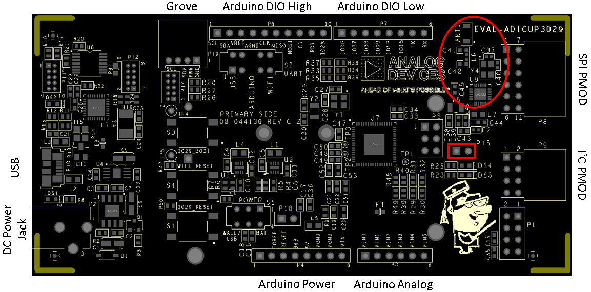
The BLE on the ADICUP3029 has a chip antenna on board, located in the upper-righthand corner. That chip antenna has been tested in open space, and can Rx/Tx packet information up to 15m.
Note
Powering the BLE Chipset
In order to use the BLE function on the ADICUP3029, a shunt MUST be placed across P15.
If you are wanting to save power and your application doesn’t need BLE, you can simply remove the shunt across P15. Removing that shunt will remove power to the BLE chipset(U8).
WiFi Module
The WiFi module is a separate hardware PCB which ships with the EVAL-ADICUP3029 kit. That WiFi module PCB is a self contained 802.15 b,n,g unit, complete with WiFi stack and protocol software. Which means that the ADuCM3029 doesn’t have to be programmed with any of the WiFi protocol/stack overhead, leaving all the memory on board to be used for the sensor application.
The WiFi module uses simple AT Commands over UART in order to transfer and send data. So if you want to use the WiFi capabilities of this board, you must ensure that the UART is initialized and that the UART switch is in the “WiFi” position.(See UART Switch section for complete details)
This WiFi module is NOT developed by Analog Devices. For more information & support concerning the WiFi module please follow the links below:
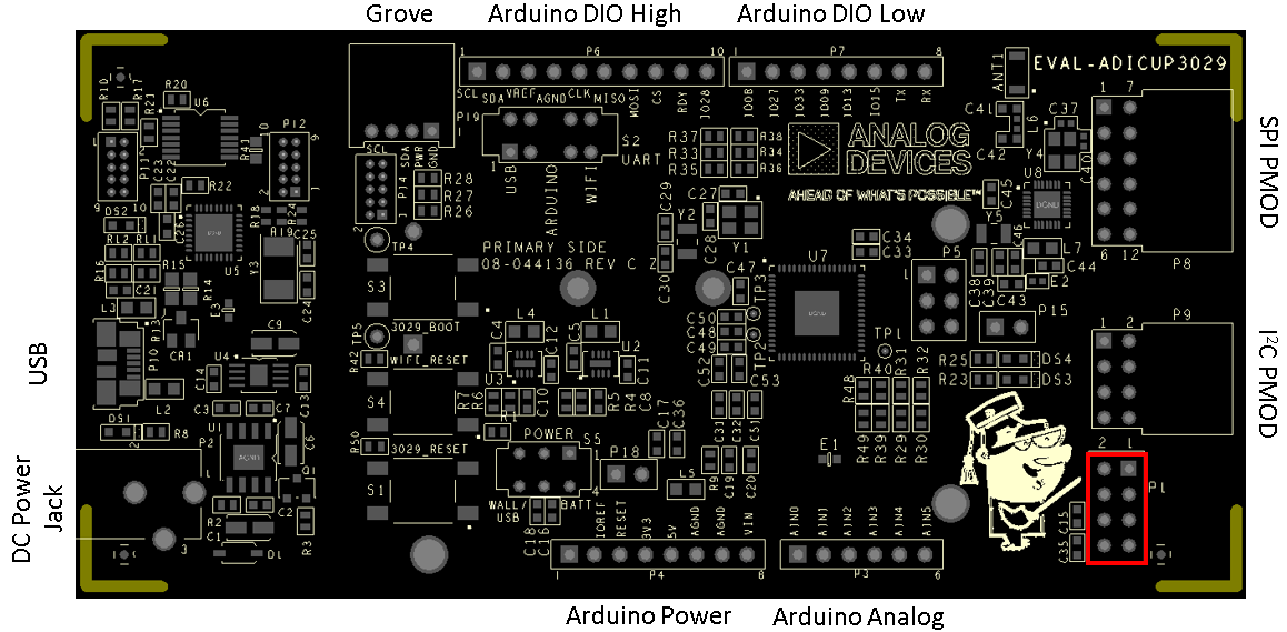
The pin out for the WiFi connector(P1) on the EVAL-ADICUP3029 and how it connects to the ADuCM3029 can be found in this table:
Pin Number |
P1 WiFi Connector Function |
ADuCM3029 Pin Name |
ADuCM3029 Port |
|---|---|---|---|
Pin 1 |
DGND |
DGND |
None |
Pin 2 |
WiFi Rx |
UART0_RX/GPIO11 |
P0_11 |
Pin 3 |
GPIO29 |
GPIO29 |
P1_13 |
Pin 4 |
GPIO42 |
ADC0_VIN7/SPI2_CS2/GPIO42 |
P2_10 |
Pin 5 |
GPIO34 |
SPT0_ACNV/SPI1_CS2/GPIO34 |
P2_02 |
Pin 6 |
WiFi Reset |
Not Connected |
None |
Pin 7 |
WiFi Tx |
UART0_TX/GPIO10 |
P0_10 |
Pin 8 |
DVDD |
+3.3V |
None |
ADICUP3029 Power Consumption Measurement
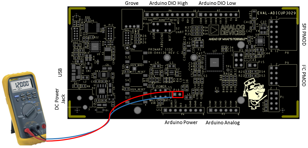
One major advantage for using the ADICUP3029, is the ultra low power operation of the ADuCM3029 microcontroller and the EM9304 low energy Bluetooth chip. We have added a jumper at P18 which will allow users to measure the amount of current flowing to all the +3.3V rails on the ADICUP3029.
The Arduino connectors, Grove connector, SPI PMOD connector, I2C PMOD connector, BLE, and WiFi connector all run off the +3.3V rail, so it makes it very convenient to measure the entire system current your solution is consuming.
Note
The on board debugger, level translator, USB connector, JTAG/SWD, external power connector, or power management devices are NOT INCLUDED when measuring the current from jumper P18 on the ADICUP3029 board.
UART Switch
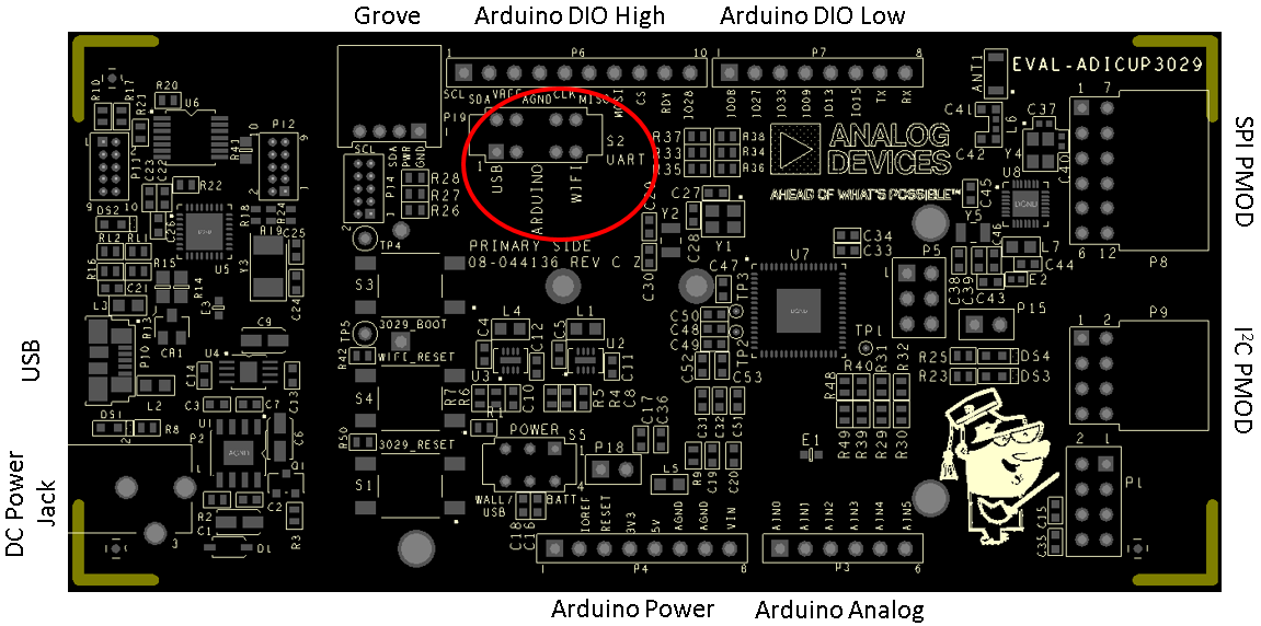
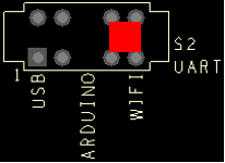
The UART is used for several functions on board the EVAL-ADICUP3029, but there is only a single UART port within the ADuCM3029. So in order to use the UART for multiple functions, switch(S2) has been placed on the board to allow the user to control what they want to use the UART for.
The UART originates from the ADuCM3029, and will communicate with three(3) external sources depending on the position of S2.
UART Function Selected |
Switch Image |
Switch Position |
Description |
|---|---|---|---|
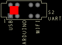
USB Port |
|
Left Position |
With switch S2 positioned all the way to the left, the ADuCM3029 will direct the UART signals to the USB connector(P10). This will effectively use the USB connector as a virtual serial terminal to your PC or laptop, Allowing the ADICUP3029 board to read and write data to the PC and display that information. |
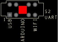
Arduino Pins |
|
Middle Position |
With switch S2 positioned in the middle, the ADuCM3029 will direct the UART signals to the Arduino connector(P7). This will allow the user to interface the ADuCM3029 with any Arduino shields that may be attached to the ADICUP3029, and need to communicate via UART. |
WiFi Module |
|
Right Position |
With switch S2 positioned all the way to the right, the ADuCM3029 will direct the UART signals to the Wifi module connector(P1). This will allow the user to interface the ADICUP3029 with the on board WiFi module (ESP8266), and start transmitting data to any nearby wireless gateways. |
Power Switch
There are three(3) ways of powering the EVAL-ADICUP3029, and a user may use any combination of power sources.
USB Powered - When connected to the PC
DC Wall Powered - When an external supply is connected to the barrel jack connector P2
Battery Powered - When batteries are connected to BT1 connector on the back of the board
Each of the different power modes, provides a different level of control and flexibility. You can find a matrix table of the different power modes and their general function here:
Power Source |
Voltage Rails Provided |
Functions/Peripherals Powered |
Notes/Comments |
|---|---|---|---|
USB Power (P10) |
5V and 3.3V |
|
|
DC Wall Power (P2) |
12V, 5V, and 3.3V |
|
|
Battery Power (BT1) |
5V and 3.3V |
|
|
USB Connector
The USB connector is primarily used for programming and debugging the ADuCM3029 from the PC and interactive development environment.
The secondary function of the USB connector is to create a virtual serial terminal connection from the PC to the ADuCM3029. In order to use this function, you must ensure that the UART switch on the ADICUP3029 is in the USB position, and that the IDE tools and PC are using this feature. Please see the UART Switch section for more information.
Push Buttons
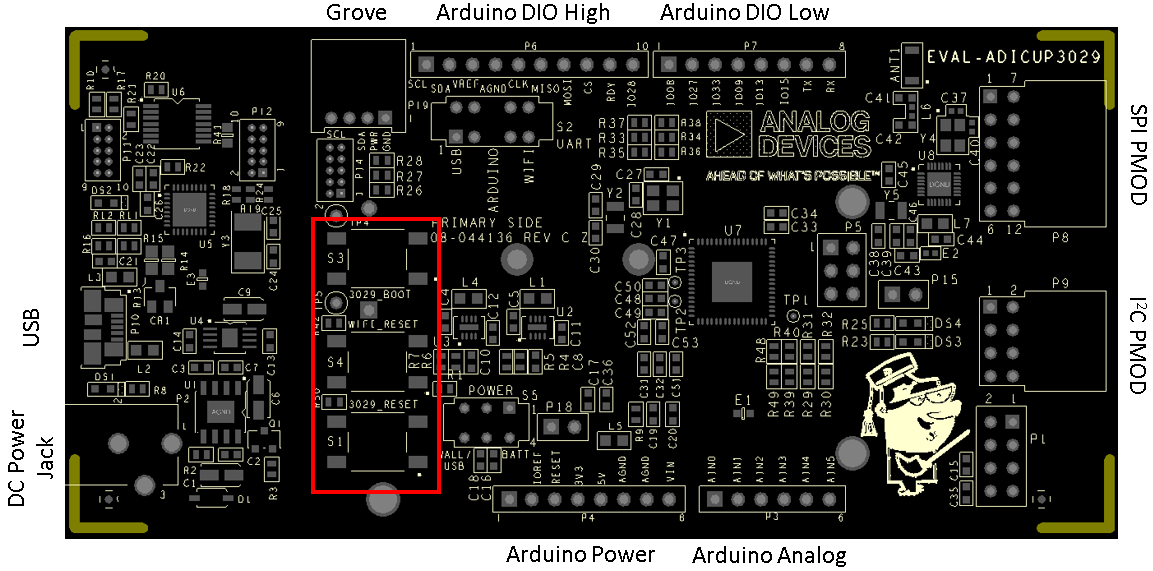
The EVAL-ADICUP3029 base board provides three buttons for use: 3029_RESET, 3029_BOOT, and WIFI_RESET.
Button |
Function |
|---|---|
3029_RESET |
Provides a hardware RESET to ADuCM3029 microcontroller. If the RESET line is connected to the Debug adapter, this button is used to invoke the Debug emulator’s Maintenance mode, where updates to the bootloader of the debug software can be made. To enter Maintenance mode, power cycle the ADICUP3029 board while pressing the RESET button. See the ADICUP3029 Driver page for more details on how to use Maintenance mode. |
3029_BOOT |
When BOOT is held down during the RESET button press and moments afterwards, the ADuCM3029 microcontroller enters UART download mode via P0_10 and P0_11. In this case, the user can download a program via the USB using the CrossCore Serial Flash Programmer tool, just make sure the UART switch (S2) is in the correct “USB” position.(See UART Switch section for more details) |
WIFI_RESET |
Provides a hardware RESET to the ESP8266 WiFi module, in case the protocol stack on the module stops transmitting for any reason. |
Programming Connectors on the ADICUP3029
There are three(3) connectors on the ADICUP3029 used for programming the on board MCUs.
P11 - JTAG Interface used to program the MK20DX128VFM5
P12 - SWD Interface used to program the ADuCM3029
P14 - SWD Interface used to program the ADuCM3029
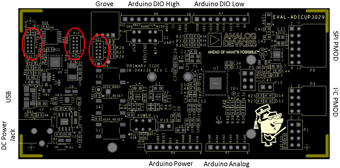
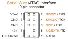
All three connectors used are based off the 10-pin ARM Cortex standard pin out(0.05” pin spacing). That pin out is common to both JTAG and SWD debug modes and is depicted in the following image.
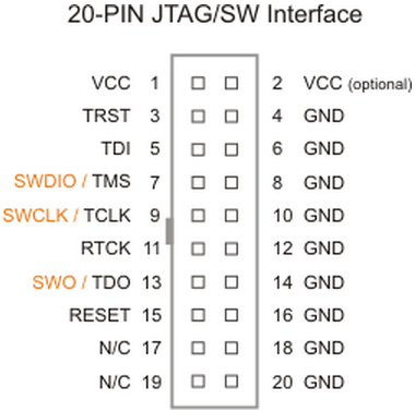
Many debugger tools (such as Segger J-Link) will typically only provide the 20-pin ARM connector(0.1” pin spacing) as an output. This connector has many of the same pins as the 10-pin version, but also provides other non essential functions for JTAG or SWD MCU devices. So you may have to do a translation from the 20-pin connector to the 10-pin connector using an adaptor. The following image shows the 20-pin connector pin out:
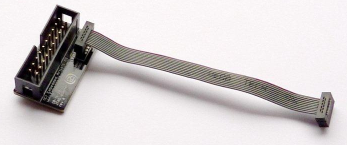
And here is an example image of a 20-pin to 10-pin adapter system.
Note
This is only an example of adapter hardware, there are many other 3rd party hardware setups that can be used to go from 20-pin to 10-pin format.
You may be asking yourself, why provide two(2) different connectors(P12 and P14) that go to the ADuCM3029 over SWD. We support a mode on the ADICUP3029 board that allows customers to break off the debugger board, so you can remotely place IoT nodes without using the debugger board. More details about this option, and how to use it, can be found by looking at the Stand Alone Mode section.
Stand Alone Mode
Using the ADICUP3029 in stand alone mode is OPTIONAL and needs carefully consideration of the trade offs before separating the debugger board from the ADICUP3029 node board. Once the two boards are split apart, there is no way to connect them back together, and return the board to its previous mode of operation. Below is a table which outlines some of the pros and cons of breaking the boards apart.
Consider this Parameter |
Benefits |
Drawbacks |
|---|---|---|
Power Source |
* Power/current consumption of the ADICUP3029 node board only * More inline with what deployed IoT nodes use for power |
* Can never again use the USB/Wall option on switch (S5) to power the ADICUP3029 node * Arduino shield add-on modules needing 7V - 12V (or VIN on P4) will not work once boards are split |
UART Destination |
* UART is still available to go to the WiFi module or the Arduino connector |
* USB port on a PC can no longer be used as a virtual serial port, to output data from ADICUP3029 node |
Ribbon Cable Connection |
* Still connect to debug and program the ADICUP3029 node board using the debugger board * Uses a standard 10-pin ARM pin out connector, so it’s easy to find and inexpensive * Should be able to use debugger board as universal CMSIS-DAP emulator board, needing only the interface file loaded into the “Maintenance” drive |
* No longer simple connection to the PC via a USB cable to debug or re-program * Need to purchase an additional connector if you want to re-program your ADICUP3029 node board |
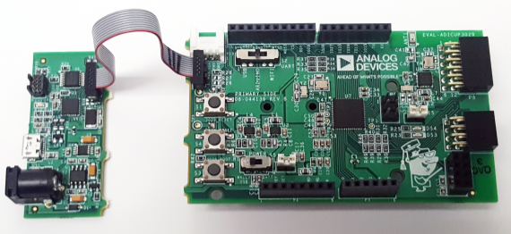
If you decide to operate the ADICUP3029 in stand alone mode, you will need to “snap” off the debugger board along the perforation provided.(May need to score it with a sharp knife first)
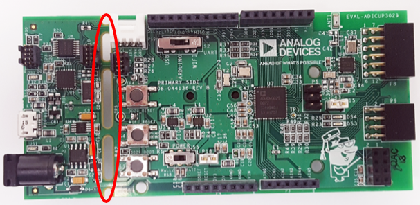
You’ll be left with two separate boards, the left hand side will be the “Debugger board” and the right hand side will be the “ADICUP3029 node board”
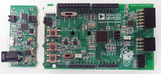
Once apart, the user can use the debugger board, and a standard 10-pin ARM JTAG/SWD ribbon cable to connect to the ADICUP3029 node board. And using the CrossCore Embedded Studio IDE, program an updated or new application into the ADICUP3029 IoT node.
Important
The debugger board will need to be plugged in via the USB port in order to program any board. And in order to program the ADICUP3029 node board, that board must be powered by (2) AAA batteries and the power switch in the BATT position. Otherwise there will be no connection between the two boards, and the mass storage device on the debugger board will come up in “Maintenance” mode.
Schematics, PCB Layout, Bill of Materials
Download
EVAL-ADICUP3029 Rev C Design and Integration Files
Schematic
PCB Layout
Bill of Materials
Allegro Project
End of Document