Hardware Guide
Overview
The board is intended to complement ADALM2000 and other standard laboratory equipment. It provides analog input and output access, digital output functions, power supplies, sensors, controls, LEDs, display connectivity, a transceiver interface, adjustable voltage references, and current-source functions. Arduino UNO R4 support adds a programmable control layer for menu-driven operation, calibration routines, signal-generator control, and embedded-system exercises.
Board Features
ADALM2000 companion education board for hands-on mixed-signal learning and prototyping
Extends ADALM2000 with integrated signal generation, analog and digital interfacing, sensors and user peripherals
Portable USB-powered platform that combines power supplies, adjustable references, signal generation, sensing, display support, and communication experiments on one board
Standalone Arbitrary Waveform Generator with up to ±10V maximum amplitude.
Onboard ±12V power supply rails and two adjustable DC reference generators covering ±12V DC
TTL/PWM 5V clock generator with adjustable frequency and software-controlled generator interface through Arduino UNO R4
Arduino UNO R4 plug-in option for menu control, calibration, display support, CAN communication, and firmware experimentation
Compatible with ADALM1000 / ADALM2000 active learning modules
Hardware Setup
This section presents detailed instructions on setting up the AD-M2KCOMPEDU-EBZ.
Accessible Headers and Connectors
There are a variety of on-board connectors that enable direct access to all features of the AD-M2KCOMPEDU-EBZ, thus minimizing the complexity of interconnection with external devices such as Arduino, ADALM2000, and external M5STACK Display.
Arduino
The Arduino connectors/headers are located under the AD-M2KCOMPEDU-EBZ for quick, non-invasive connections. These connectors are extended to the top of the board in a pin-to-pin arrangement, allowing direct access to all Arduino terminals.
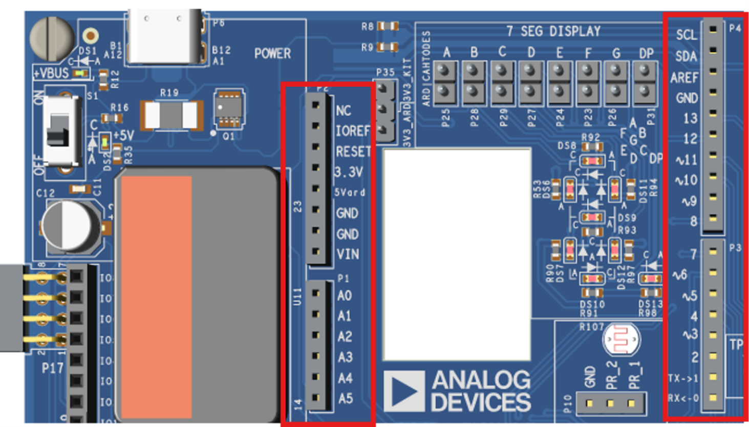
Additionally, the AD-M2KCOMPEDU-EBZ features a PCB window that provides a clear view of the Arduino 8x12 LED matrix.
Note
The Arduino has its own USB port used for power supply and configuration. However, this USB port does not provide power to the AD-M2KCOMPEDU-EBZ. The Arduino can only receive power from the module’s 5V bus due to the presence of diode D6. See figure below.
This arrangement allows both USB ports to be connected to power supply/laptop without interfering, enabling “live programming”.
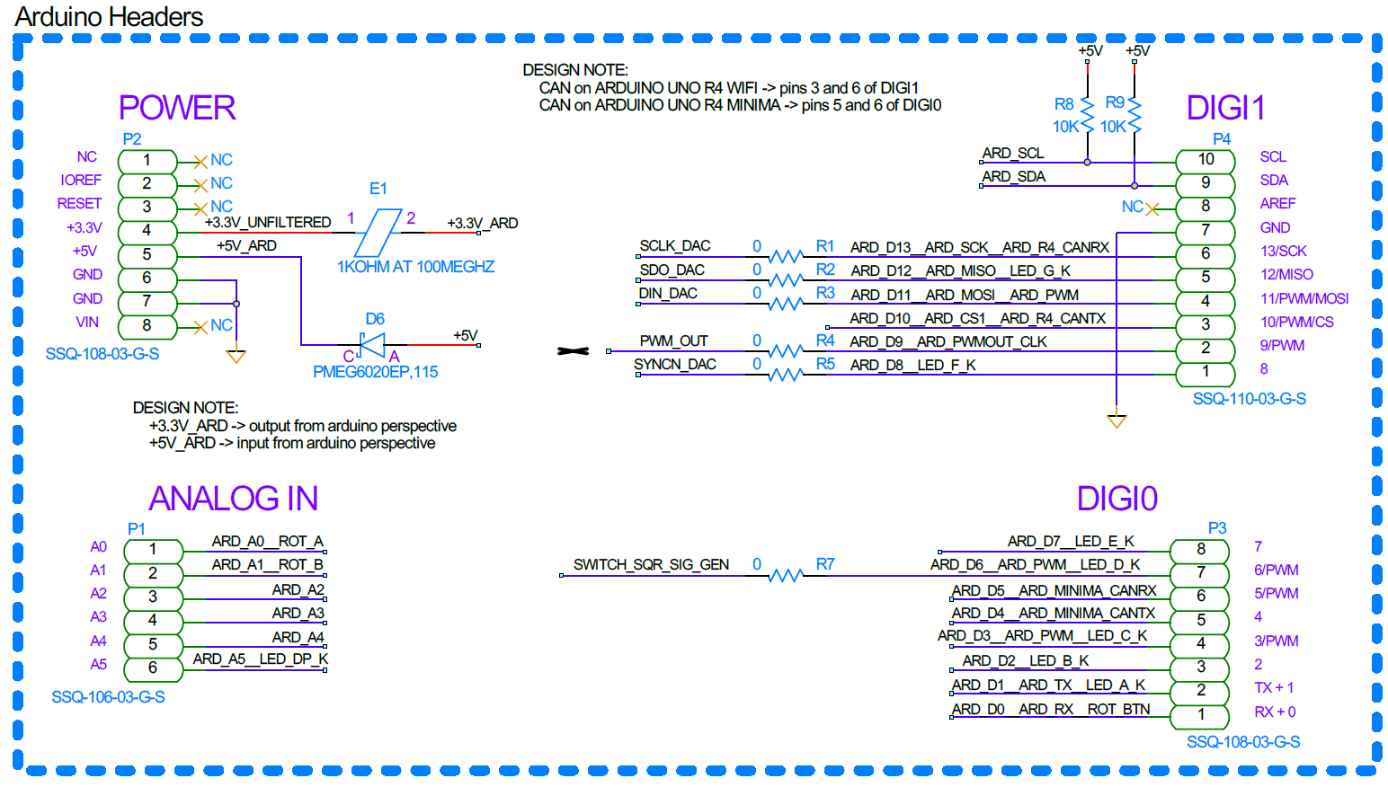
Note
Although the user has access to all Arduino terminals, please note that some of them are already connected to the AD-M2KCOMPEDU-EBZ onboard devices, so they should not be used otherwise.
For instance, the SPI port is already connected to the AD9833 signal generator and the AD5443 DAC. However, only the SS/CS lines are reserved, therefore more SPI devices can be connected to the port, with other SS/CS lines.
In a similar manner, the I2C port connects to the display and the AD5625 DAC. However, more I2C devices can be connected to it, if the devices I2C addresses do not conflict with the existing ones (0x3C for the display and 0x1E for AD5625).
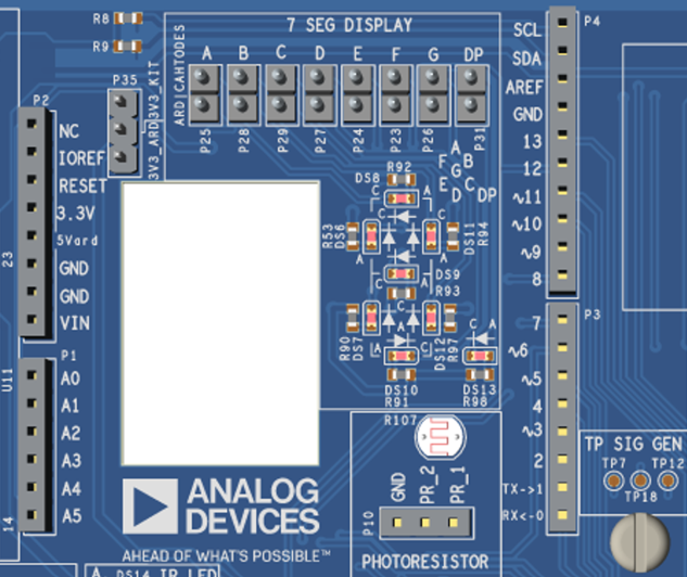
The list of Arduino ports already used and/or reserved by the AD-M2KCOMPEDU-EBZ functionality is presented in the table below:
Arduino Pin goes to |
AD-M2KCOMPEDU-EBZ |
Notes: IN/OUT wrt Arduino |
||
|---|---|---|---|---|
Net name |
Connector |
Pin |
||
SCL |
ARD_SCL |
P4 |
10 |
Pulled-Up to 5V with 10K, shared I2C line; use only with compatible I2C devices. |
SDA |
ARD_SDA |
P4 |
9 |
Pulled-Up to 5V with 10K, shared I2C line; use only with compatible I2C devices. |
A0 |
ARD_A0__ROT_A |
P1 |
1 |
Dig Input: Menu rotary encoder signal. Pulled-up to 5V with 10K. |
A1 |
ARD_A1__ROT_B |
P1 |
2 |
Dig Input: Menu rotary encoder signal. Pulled-up to 5V with 10K. |
RX + D0 |
ROT_BTN |
P3 |
1 |
Dig Input: Menu rotary encoder push button. Pulled-up to 5V with 10K. |
D6/PWM |
SWITCH_SQR_SIG_GEN / LED_D_K |
P3 |
7 |
Dig Output: SQW signal generator (SG) attenuator. Controls U1 ADG444 switch. |
D13/SCK |
SCLK_DAC / ARD_D13_ARD_SCK_ARD_R4_CANRX |
P4 |
6 |
SPI port clock signal. Already connected to the signal-generator devices. Also shared with CAN RX when CAN jumpers are used. |
D12/MISO |
SDO_DAC / ARD_D12_ARD_MISO_LED_G_K |
P4 |
5 |
SPI MISO / SDO signal. Already connected to signal-generator devices. Also connected to 7-segment LED G cathode when jumper is used. |
D11/PWM/MOSI |
DIN_DAC / ARD_D11_ARD_MOSI_ARD_PWM |
P4 |
4 |
SPI MOSI / data input, already connected to the signal-generator DAC. |
D10/PWM |
ARD_D10_ARD_CS1_ARD_R4_CANTX |
P4 |
3 |
Reserved as chip-select for the onboard signal generator. Also shared with CAN TX when CAN jumpers are used. |
D9/PWM |
PWM_OUT / ARD_D9_ARD_PWMOUT_CLK |
P4 |
2 |
Reserved: PWM output of the hex inverting Schmitt trigger / CLK buffer. |
D8 |
SYNCN_DAC / ARD_D8_LED_F_K |
P4 |
1 |
Reserved for signal-generator DAC sync/chip-select control. Also connected to 7-segment LED F cathode when jumper is used. |
The remaining Arduino pins are either available or conditionally available to the end user, depending on the selected AD-M2KCOMPEDU-EBZ functions.
Note
Arduino reserved pins/ports have double functionality that serves the AD-M2KCOMPEDU-EBZ in the following use cases:
Sig Gen Control: Priority 1. All Sig Gen controls are directly connected to the Arduino header; no jumpers are required.
CAN RX/TX config: Priority 2, all CAN RX/TX pins can be connected to Arduino header via dedicated Jumpers P21, P22.
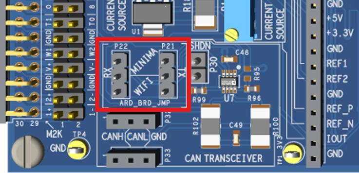
7 Segments LED display control: Priority 2, all LED cathodes can be connected to Arduino header via dedicated Jumpers P23, P31.
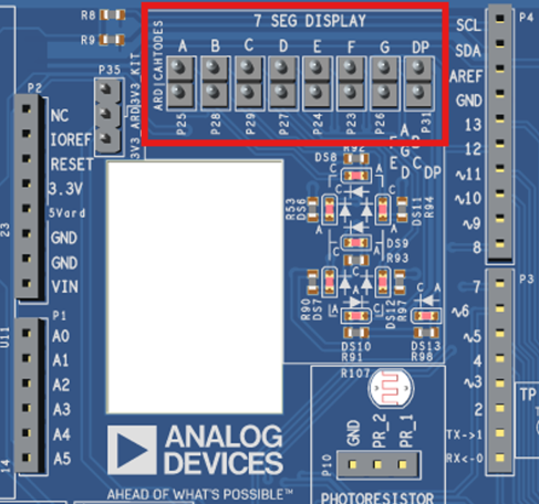
Figure 5 7-Segment Display Cathodes to Arduino Connection Jumpers P23-P31
Thus, only one use-case is recommended to be used at a time to avoid inputs/outputs overdrive.
The Arduino pins not listed as already connected or reserved may still be conditionally assigned to optional AD-M2KCOMPEDU-EBZ functions, such as CAN or the 7-segment display. The table below lists the Arduino header pins that are available or conditionally available to the end user.
Arduino Pin goes to |
AD-M2KCOMPEDU-EBZ |
Notes: IN/OUT wrt Arduino |
|
|---|---|---|---|
Port |
Pin |
||
ARD_A2 |
P1 |
A2 |
Available analog input / GPIO for end-user use. |
ARD_A3 |
P1 |
A3 |
Available analog input / GPIO for end-user use. |
ARD_A4 |
P1 |
A4 |
Available analog input / GPIO for end-user use. |
ARD_A5 |
P1 |
A5 |
Available only if the 7-segment decimal point connection is not used. |
NC |
P2 |
1 |
NC |
IOREF |
P2 |
2 |
Arduino IO reference pin; not used by AD-M2KCOMPEDU-EBZ circuitry. |
RESET |
P2 |
3 |
Arduino RESET pin; not used by AD-M2KCOMPEDU-EBZ circuitry. Not a GPIO |
+3.3V |
P2 |
4 |
Arduino +3.3V unfiltered. |
+5V |
P2 |
5 |
Arduino +5V, D6 cathode, 250mV lower than AD-M2KCOMPEDU-EBZ +5V bus if Arduino USB or power jack is not plugged in. |
GND |
P2 |
6, 7 |
Arduino GND. |
VIN |
P2 |
8 |
Arduino VIN header pin; not connected to AD-M2KCOMPEDU-EBZ circuitry. |
D1/TX |
P3 |
2 |
Available only if 7-segment LED A cathode is not used. |
D2 |
P3 |
3 |
Available only if 7-segment LED B cathode is not used. |
D3/PWM |
P3 |
4 |
Available only if 7-segment LED C cathode is not used. |
D4 |
P3 |
5 |
Available only if the CAN function for Arduino is not used. |
D5/PWM |
P3 |
6 |
Available only if the CAN function for Arduino is not used. |
D7 |
P3 |
8 |
Available only if 7-segment LED E cathode is not used. |
GND |
P4 |
7 |
Arduino GND. |
ARE |
P4 |
8 |
Arduino AREF. |
Working in conjunction with ADI ADALM2000
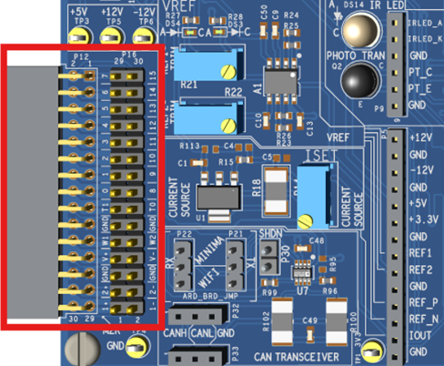
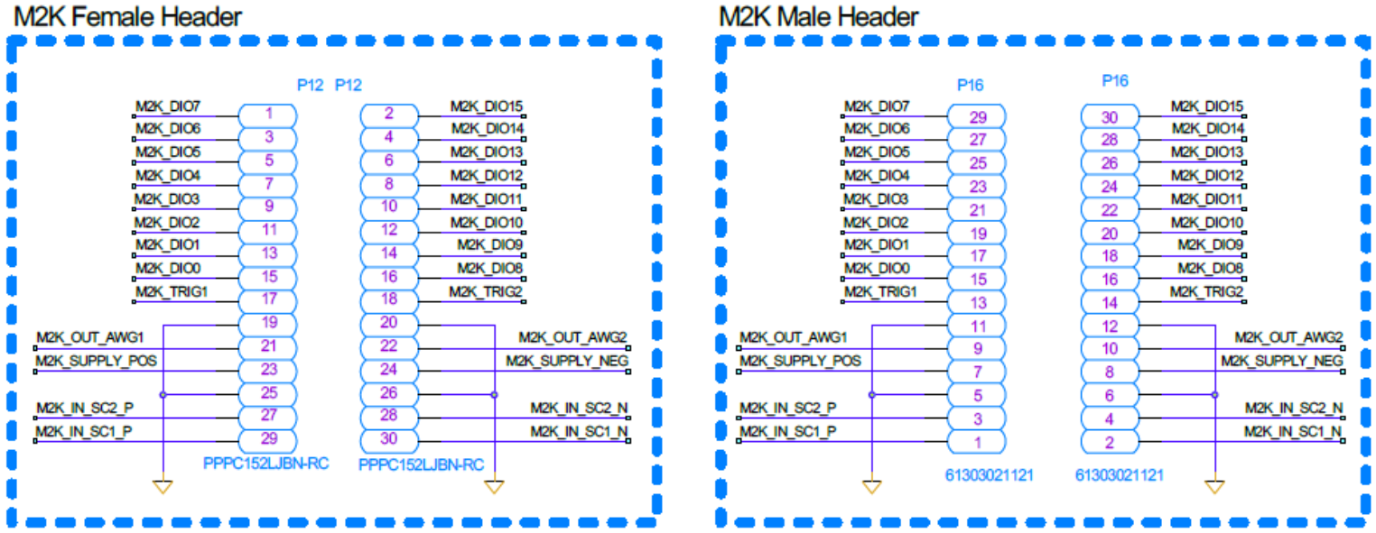
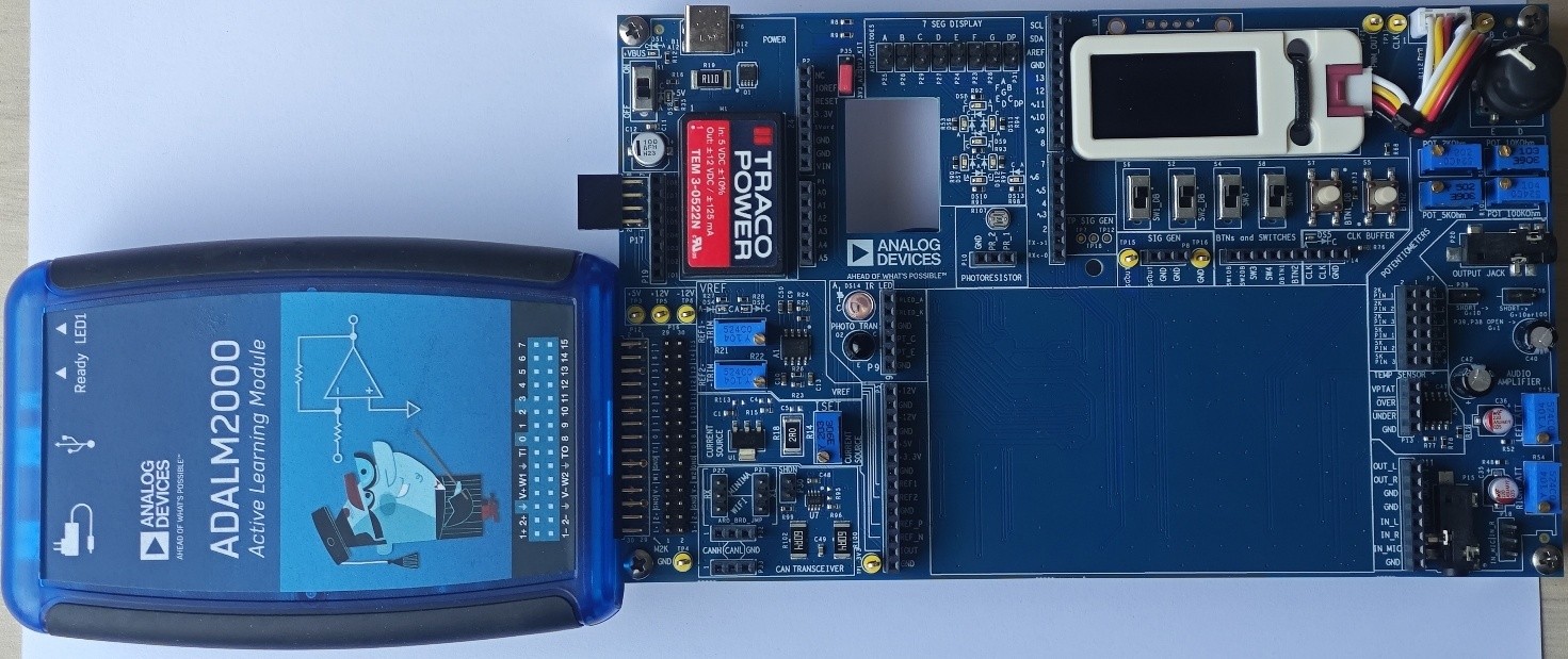
The ADALM female connectors/headers P12 is located on the left of the AD-M2KCOMPEDU-EBZ for quick, non-invasive plug-in connections. A male type of connector (P16) is placed right next to it, in a pin-to-pin vertical mirror arrangement, allowing direct access to all ADALM ports.
|
|
External M5STACK Display
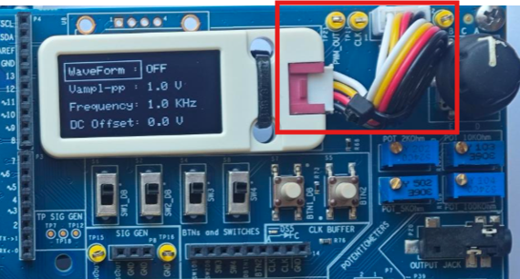
There is a dedicated connector for an additional M5STACK Display P34.
Note
A HY2.0-4P cable is necessary.
Generic Jumpwire IO bridge (P17 + P19)
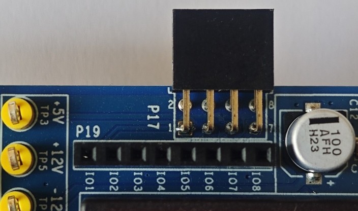
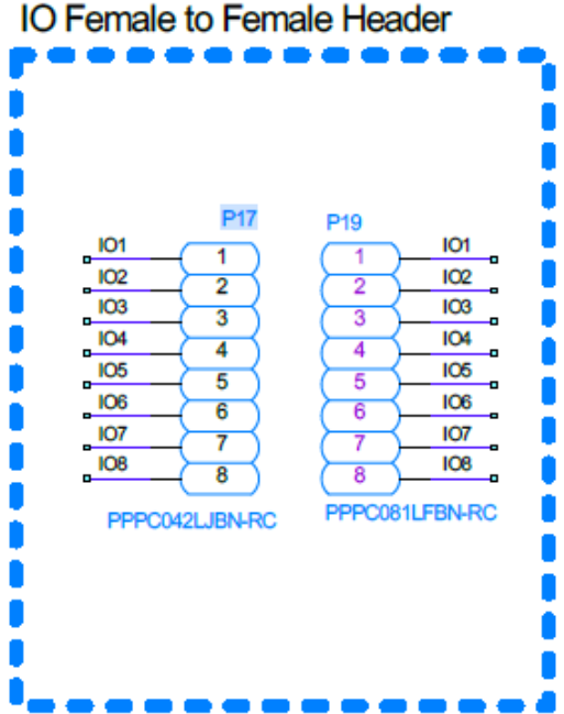
The AD-M2KCOMPEDU-EBZ board includes two 8-pin female headers (P17 and P19), connected pin-to-pin. These connectors form a generic jump-wire IO bridge that can be used to route user-defined signals or external connections across the board.
All eight IO bridge lines are available for end-user configuration. Since these lines are not assigned to a fixed onboard function, the user must verify the signal source, voltage level, and direction before connecting external circuitry.
Power supplies of the AD-M2KCOMPEDU-EBZ board
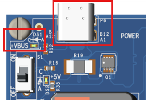
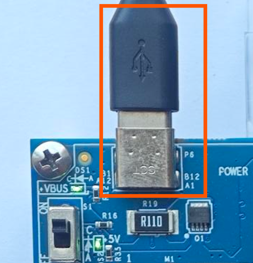
The AD-M2KCOMPEDU-EBZ is supplied from a +5V USB source through the USB Type-C connector P6.
Connect the USB-C cable from a standard phone charger (min 1A) to the USB Type-C port named P6 on the board. Green LED DS1 (+VBUS) indicates the presence of input power supply.
Power ON the AD-M2KCOMPEDU-EBZ via S1 slide switch. When S1 is switched to “ON” position, the Green LED DS2 (+5V) lights up indicating that +VBUS power is delivered to the Board +5V.
Note
If DS2 LED does not light up when S1 is in ON position, the over current protection may have been triggered, or the input power supply is no longer available—check DS1 LED status!
Over current protection (OCP) threshold is set at 900mA. In the event of an OCP, the board is auto powered OFF. Remove the Load/short-circuit from the 5V Supply and power OFF the board. A power ON/OFF/ON cycle is required to reset the OCP.
Note
Do not short the +5V_ard with the 5V bus, as this will bypass the anti-reverse supply diode D6. This may cause interference between the two USB power suppliers: Charger/PC-Laptop (assuming that the Arduino board is connected to a PC/Laptop). Moreover, the 5V bus is no longer protected by the AD-M2KCOMPEDU-EBZ onboard OCP circuit and it will take power from 5V_ard bus.
Caution
Power the AD-M2KCOMPEDU-EBZ from a 5V USB charger, a standard phone charger, or a PC/laptop USB port.
Normal operation: Green LED D12 continuously lit; Red LED D6 off
Caution
Current limit: LED DS2 blinking: The 900mA current limit is reached. Remove the USB-C cable from P6 USB Type C receptacle and check the schematic on the breadboard in order to find a possible short circuit between power rails (for example 5V shorted to ground or 12V shorted to ground) or a high current path (the total current consumption must be under 900mA)
Warning
The current limiter Q1 NMOS switch gets hot during short circuit! DO NOT TOUCH! Touching it can result in a HAZARD.
Available Fixed Power supply outputs
The power consumption of AD-M2KCOMPEDU-EBZ is limited to 4.5W from the 5V USB supply. The current consumption is limited to 900mA. The AD-M2KCOMPEDU-EBZ provides:
+5V supply rail
Two +3.3V from Arduino AND/OR Local LDO
±12V symmetrical supply rails
The 5V supply rail
The maximum available power at the 5V supply rail is 3.5W (5V·700mA). The AD-M2KCOMPEDU-EBZ quiescent current is approximately 200mA, that leaves the user with approx. 700mA available current.
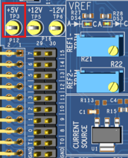
The 5V supply rail is accessible at the female port P5/5 and TP3.
LED DS2 GREEN lit indicates the normal operation of the 5V VCC power supply.
Note
The 5V supply rail is not regulated on board, thus the voltage level is determined by the USB VBUS. This was found to be in the range of 4.8V up to 6V, depending on the USB power supply.
Note
The voltage level at this pin is not regulated on board, it is determined by the VBUS+ level at the USB-C.
Two options for the +3.3V supply rail
The AD-M2KCOMPEDU-EBZ provides two possible sources for the +3.3V supply rail. The active source is selected using the P35 selection jumper. The +3.3V rail can be supplied either from the Arduino board or from an onboard LDO. The +3.3V rail selected by the P35 jumper is then used to power all the +3.3V auxiliary circuitry on the AD-M2KCOMPEDU-EBZ (Audio Amp, 20MHz CLK, Programmable Waveform Generator).
Note
The signal generator functions only if the P35 jumper is present, connecting the mid-pin with one of the side pins. It is recommended to supply the signal generator from the onboard LDO, connect the P35 jumper to the top pin, denoted 3V3_KIT, as this provides a more stable and noise-free power supply than the 3V3_ARD line.
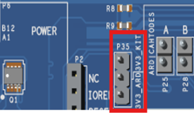
Figure 15 P35 +3.3V Supply Source Selection Jumper: PCB View |
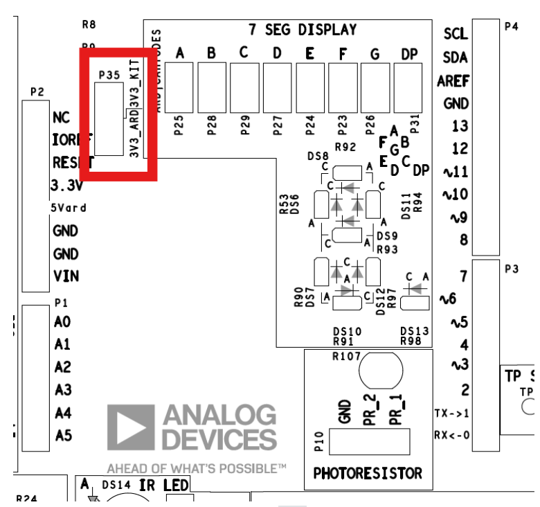
Figure 16 P35 +3.3V Supply Source Selection Jumper: Schematic View |
Arduino +3.3V rail
The +3.3V_ARD supply rail is provided by the Arduino via port P2/4, thus it is available only if the Arduino is connected to the AD-M2KCOMPEDU-EBZ. This rail is regulated by the Arduino local LDO and has a current capability of about 30mA. The Arduino provides overcurrent/short circuit protection, but such an event might cause the Arduino to shut down or reset.
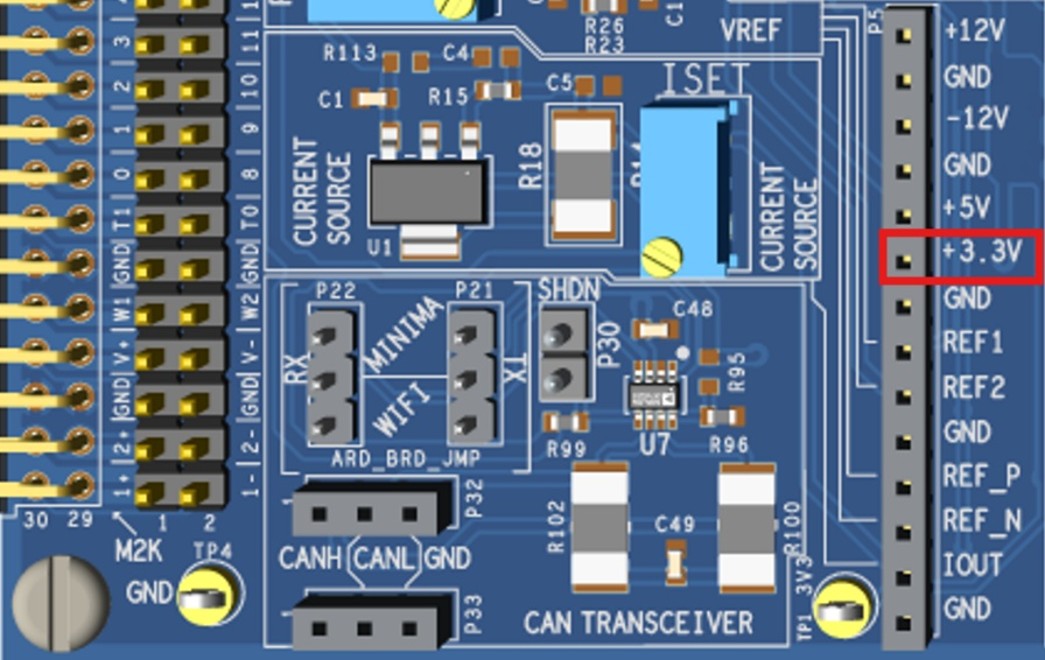
The onboard 3.3V LDO (ADM7150ARDZ-3.3)
The AD-M2KCOMPEDU-EBZ also includes an onboard +3.3V LDO, implemented with the ADM7150ARDZ-3.3; it has a current capability of maximum 800mA. This supply option allows the board to generate its own regulated +3.3V rail, independently of the Arduino +3.3V output. The onboard LDO that powers the +3.3V_KIT line.
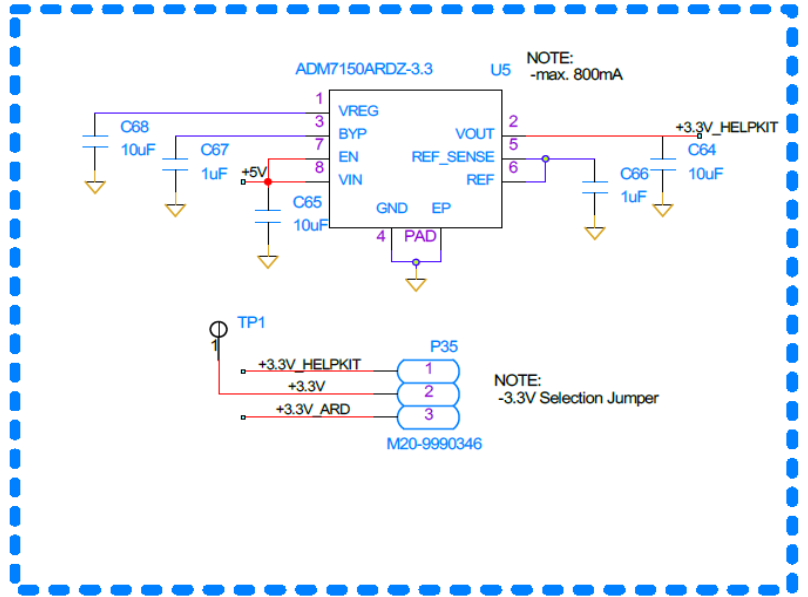
Figure 18 +3.3V Local LDO and P35 Selection Jumper: Schematic view
The ±12V symmetrical supply rails
The ±12V Rails are generated locally/onboard by the M1 circuit (TEM 3-0522N) that is a fully integrated Switched-Mode Power Supply with fixed output voltages at +12V and -12V with a current capability up to 125mA per rail.
Note
The available current for these supply rails is lower than 125mA because the rails also supply onboard circuitry.
LEDs DS3 and DS4 lit GREEN indicate the “OK” status of the ±12V supply:
LED DS4 (green): When lit, it indicates the presence of +12V supply rail.
LED DS3 (green): When lit, it indicates the presence of -12V supply rail.
Note
The LED voltage drops are used as reference for the ±12V Reference voltage generator/buffers described in the Adjustable Voltage and Current references section. The ±12V supply rails are available for the user at P5 connector, pins 1 and 3, and TP5 and 6.
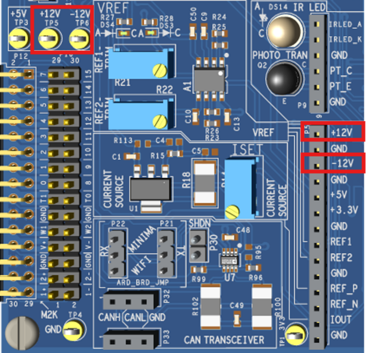
Figure 19 ±12V Symmetrical Supply Rail Connector TP and Pin Location
Ground pins
There is a single ground plane, common for all analog and digital sections, also with the Arduino and ADALM interfaces.
Multiple GND pins, both male and female, are available across the AD-M2KCOMPEDU-EBZ board. Additional test pins are also provided on the board for measurement and debugging purposes.
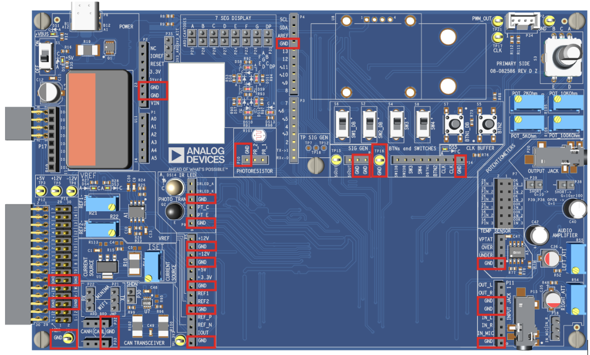
Figure 20 TP and Pin Location GND provides access to Board Ground
Adjustable Voltage and Current references
There are two adjustable voltage references and one current source reference available onboard for the end-user:
Adjustable VREF_DC [-12V, +12V] range
The AD-M2KCOMPEDU-EBZ has two adjustable DC reference voltage outputs, REF1 and REF2. They are adjustable via the trimmers multiturn resistors R21 and R22 in the [-12V, +12V] range. Turn clockwise to increase the reference voltage.
Note
VREF outputs are low impedance outputs driven by an ADA4511-2 op amp that can drive up to 22mA of load (sink or source) in normal operation conditions and 60mA in short circuit conditions.
These Adjustable VREF_DC are derived from two references/fixed voltage levels obtained from the power supply status LEDs DS3 and DS4, VLED_FORWARD, dropout referred to GND. They are denoted as REF_P and REF_N and have typical values of +1.9V and -1.9V respectively. A fixed gain factor of 6.4V/V is used to amplify the non-inverting input voltage levels (INAP_REF & INBP_REF) set by the multiturn resistors connected to these VLED_FORWARD reference voltage levels.
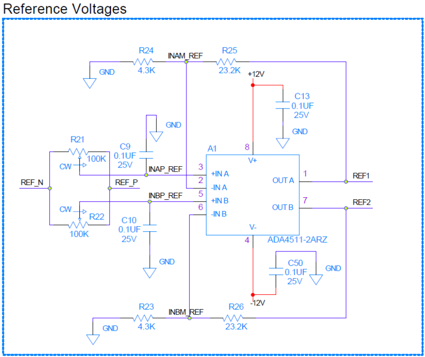
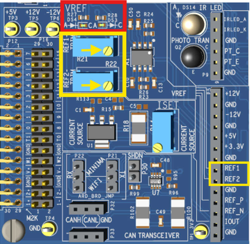
The adjustable output voltages REF1, REF2 and their reference levels REF_P and REF_N are accessible at the connector P5, pins 8 and 9, and pins 11 and 12, respectively.
DC current source with adjustable IDC between 350µA and 60mA
The AD-M2KCOMPEDU-EBZ has one reference DC current source (LT3092) adjustable in the range [350µA to 60mA]. Turn clockwise to increase the reference current.
Note
This current source is supplied from the +12V rail and has a typical dropout of 1.2V, thus can operate up to 10.8V voltage levels. The output current is filtered with a 0.22µF capacitor to ground, thus the user can expect a large inrush/initial current when connecting the source to the load, due to the charge accumulated in the filtering cap.
The adjustable current is accessible at the connector P5, pin 13.
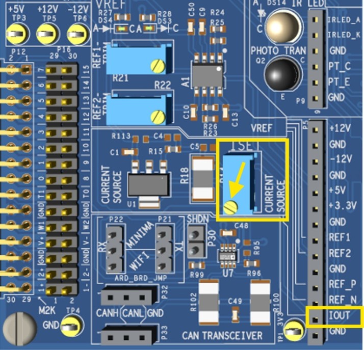
Figure 23 Adjustable Current Source Connector/Pin Location on the Board
Audio amplifier
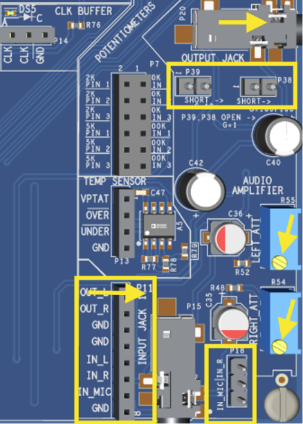
The AD-M2KCOMPEDU-EBZ includes a Headphone Audio Amplifier (AD8532) with configurable voltage gain of 1:10:100V/V for Right channel and fixed unity gain on Left channel. It also has fine trim adjustable attenuation up to 1:10V/V on both channels.
The left channel gain configuration is realized by means of Jumpers P38 & P39 while the attenuation for both channels is adjustable via multi-turn trimmers R54 and R55. Turn clockwise to increase the attenuation.
In addition, the right channel can be re-configured as a microphone amplifier via P18 jumper, thus connecting the amplifier input path to Jack input port P15 pin 4.
Note
Both the inputs and outputs are DC decoupled by means of series capacitors C35, C36 and C40 C42 respectively to operate with the asymmetric/single supply of the amplifier. Microphone input path is pre-biased with a 2.2kΩ resistor to 3.3V rail (phantom-power).
The amplifier is supplied from the +3.3V rail; thus, the user can expect a maximum output voltage excursion equal to its supply in no load conditions.
Also, the amplifier has external 15Ω output resistors (R58, R59) for short circuit protection; thus, the user can expect reduced output voltage swing when driving a heavy load (4Ω to 32Ω).
The section includes 3.5 mm female jack input and output ports, together with associated jumper pins for jumper-wire connections.
Onboard Sensors
There are two types of sensors placed on the AD-M2KCOMPEDU-EBZ available for the end-user: one temperature sensor and two light sensors (IR & LDR)
Temperature sensor
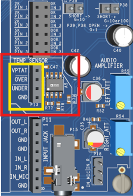
The AD-M2KCOMPEDU-EBZ includes a temperature sensor (TMP01) with an analog (VPTAT: 5mV/K) output voltage characteristic. VPTAT varies from 1.165V at −40°C to 1.79V at +85°C.
It also provides two active-low open-drain digital status outputs: \(\overline{OVER}\) and \(\overline{UNDER}\), with preset thresholds of 19°C and 29°C and hysteresis.
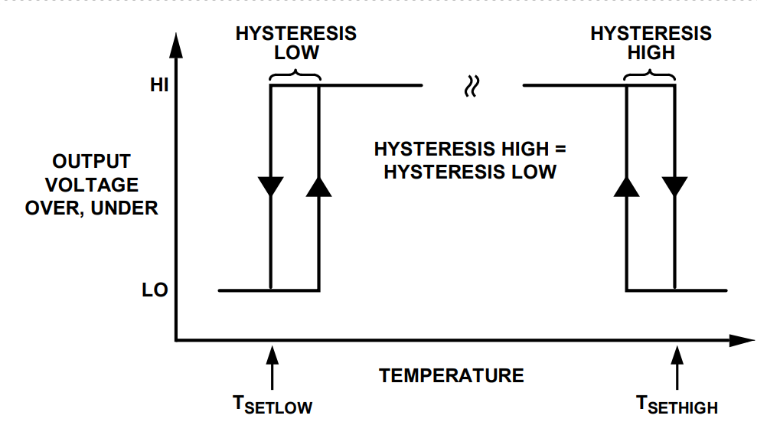
The three outputs are available to the user at P13 port.
Note
A quick sensor test can be performed by touching A5 integrated circuit package: it will trigger the \(\overline{OVER}\) status output. 4.7kΩ pull-up resistors are recommended to be used for the status outputs.
Light sensors: IR TX/RX & LDR
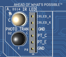
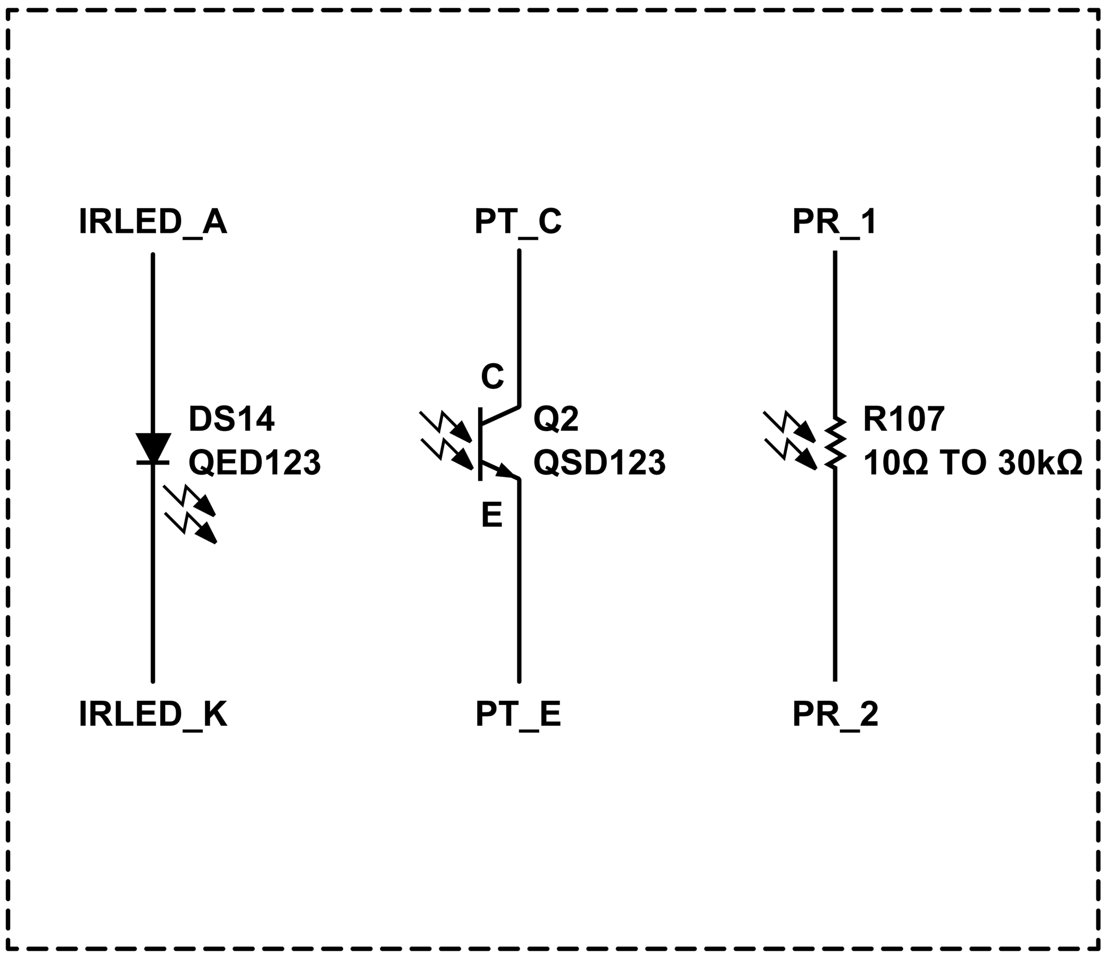
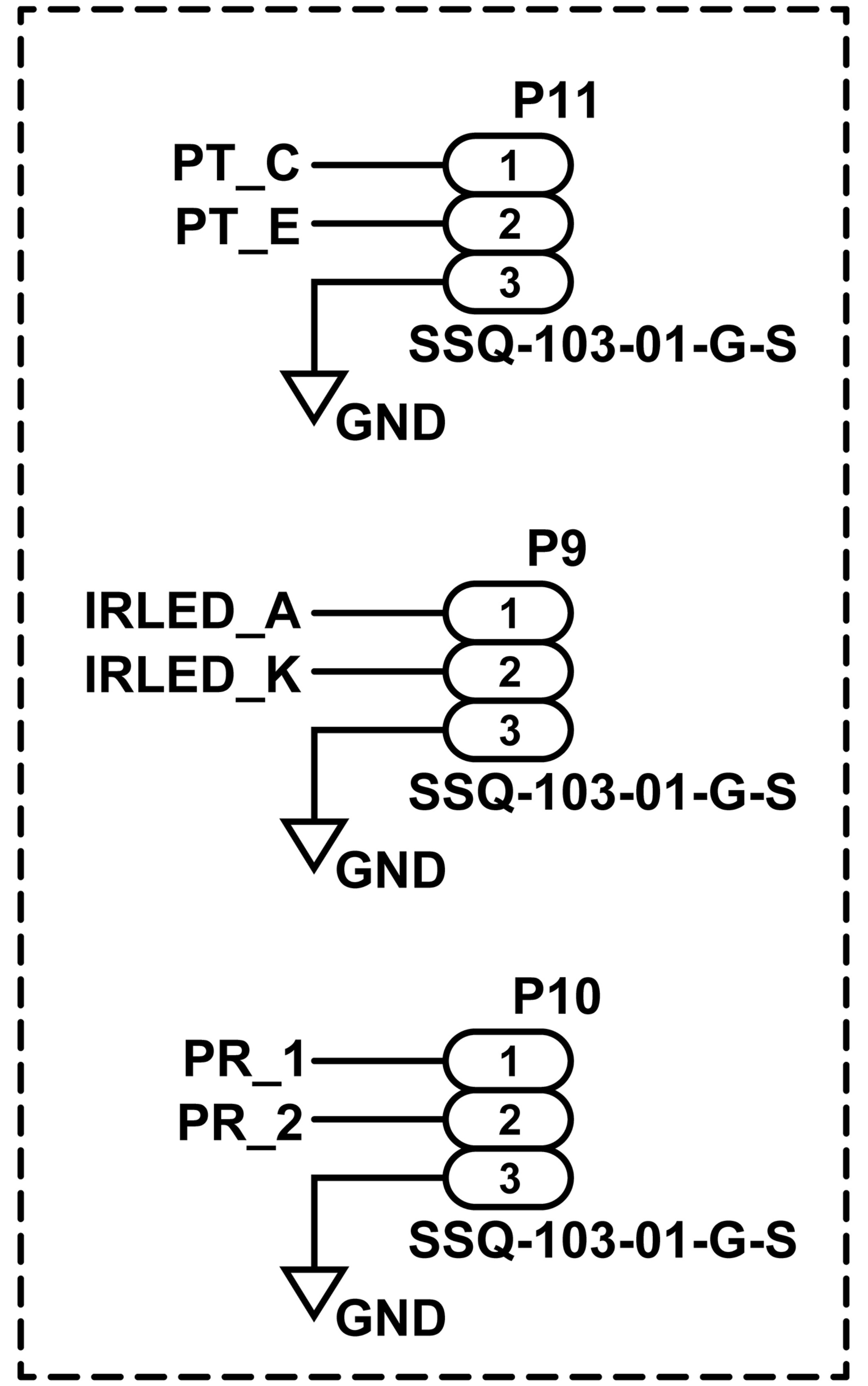
The AD-M2KCOMPEDU-EBZ includes one IR LED, one IR phototransistor, and one photoresistor for a wider light spectrum. The IR LED, IR phototransistor and photoresistor terminals are accessible through the corresponding P9 and P10 headers.
User-accessible multi-turn potentiometers
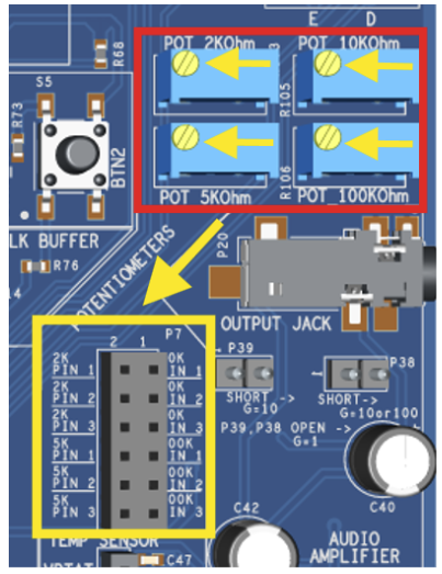
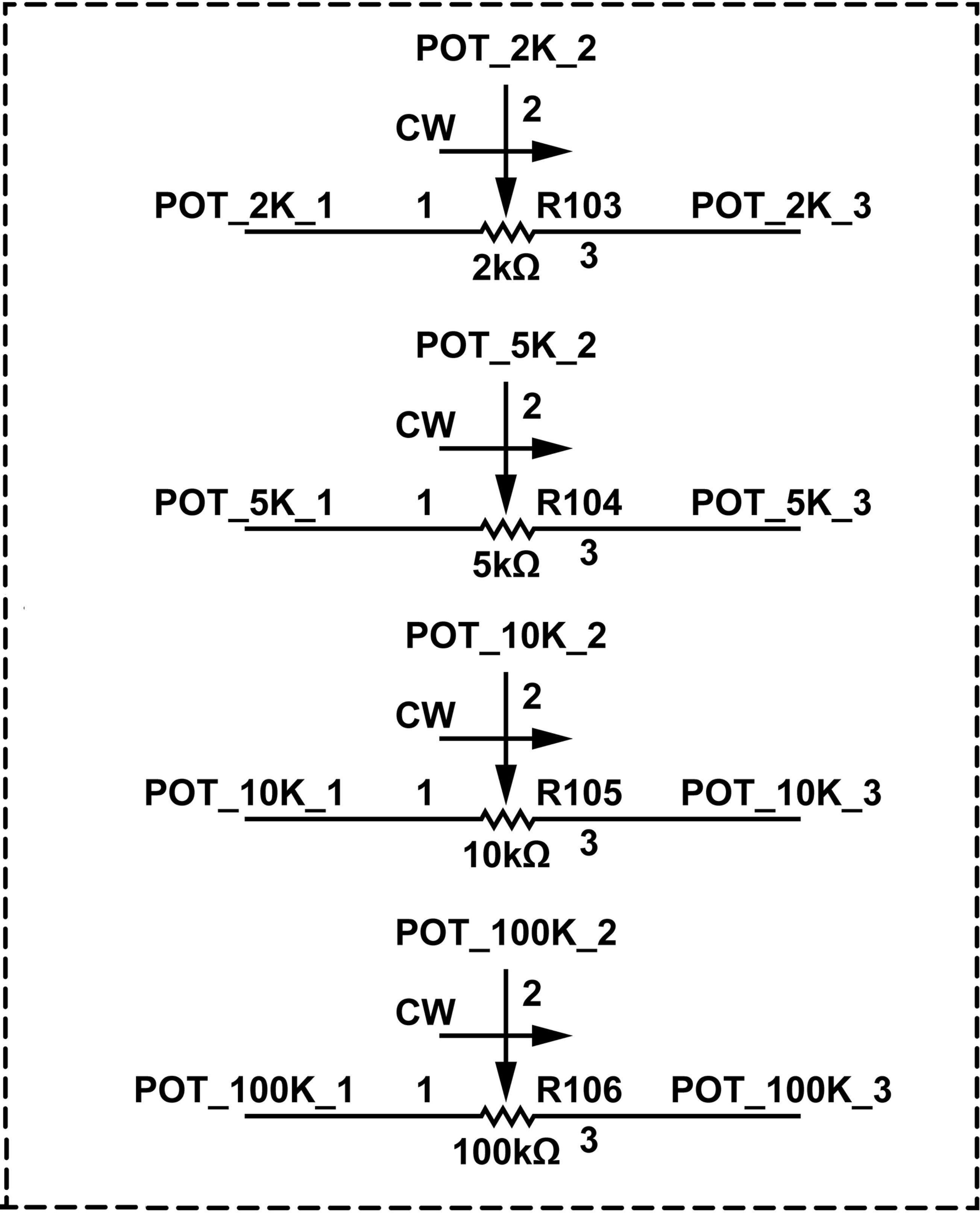
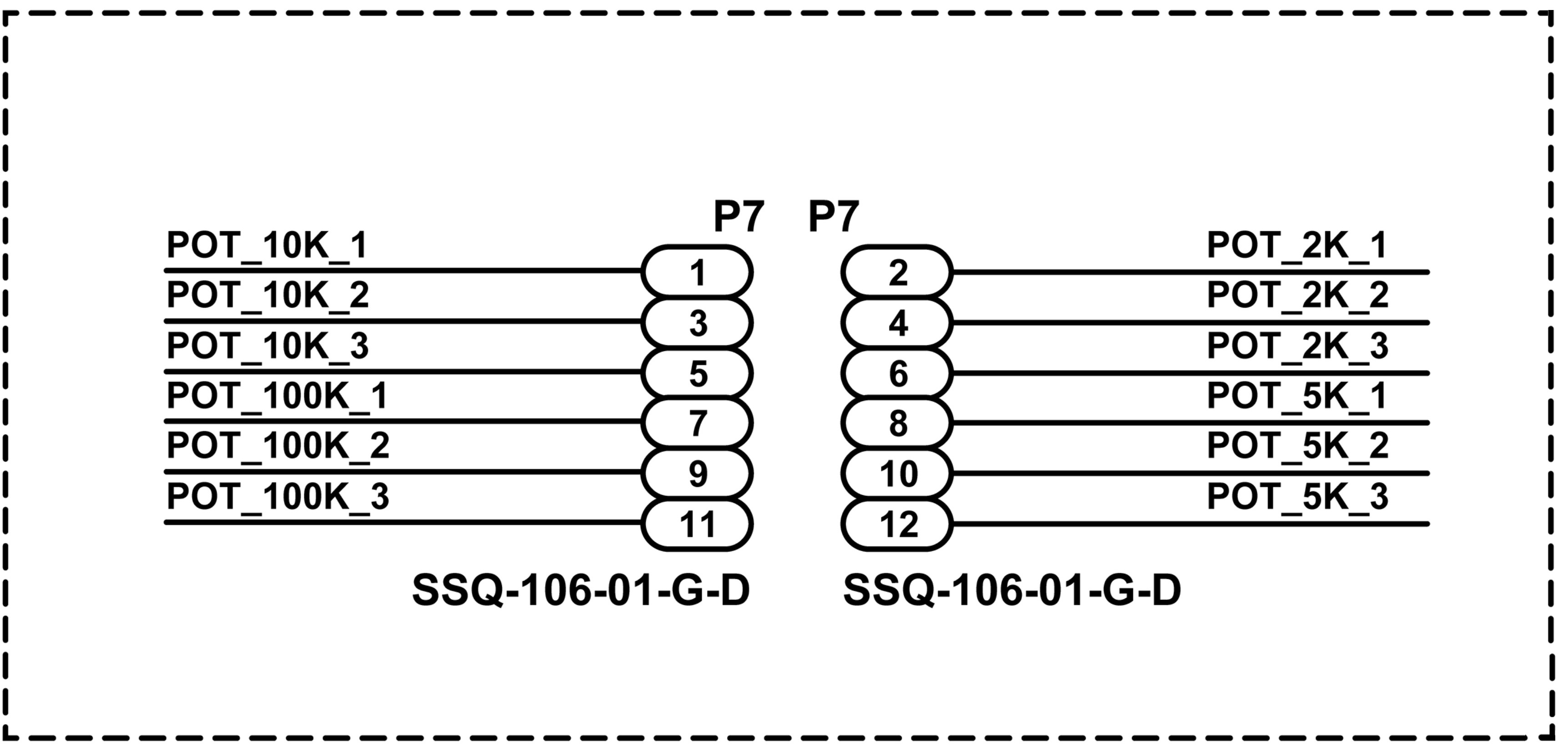
The AD-M2KCOMPEDU-EBZ includes four multiturn linear potentiometers, with all three terminals available to the user at header P7: R103 = 2kΩ, R104 = 5kΩ, R105 = 10kΩ, R106 = 100kΩ.
Digital/Binary controls
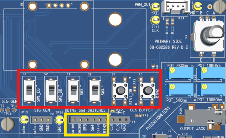
The digital control section contains six logic controls implemented with 4 slide switches (Instances S6, S2, S4, S8) and 2 tactile push-buttons (Instances S7 and S5).
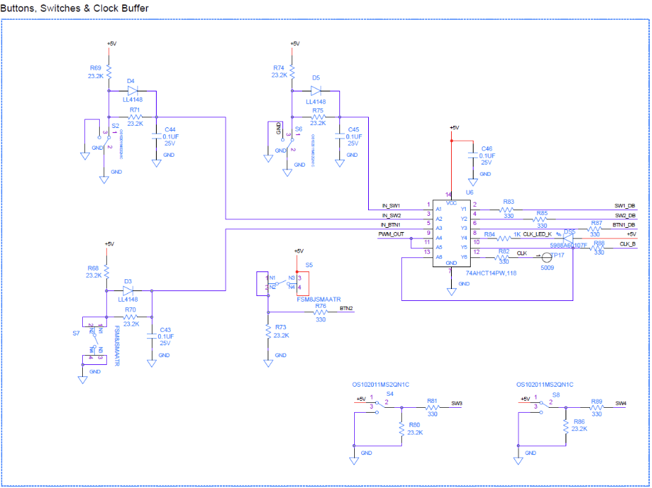
Out of the four slide switches, only the first two comprise a 1.8ms debounce circuitry (denoted SW1_DB and SW2_DB) while the last two (denoted SW3 & SW4) do not. Similar case for the tactile push buttons; the first one is debounced while the second is not.
The debounced digital controls are also buffered with HEX inverters (U6, 74AHCT14PW, 118) for enhanced switching noise immunity and low output impedance/large fanout.
Logic 0/1 is obtained as follows:
Slide switch -> slide downwards=’0’ / slide forward=’1’.
Tactile push-button -> pressed & held=’0’ / released = ‘1’.
All digital controls are 5V TTL and are current-limited to a short-circuit current of maximum 15mA per output by means of output series resistors of 330Ω.
The digital states can be monitored by using the 7 Seg LED Display (common Anode, open cathode -> lit= ‘0’ logic). Each will be lit when a logic “1” is applied to the input (J9 connector).
The digital/binary control switches and their corresponding outputs are accessible on the PCB “BTNs and SWITCHES” section.
7-Segment Display
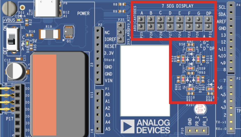
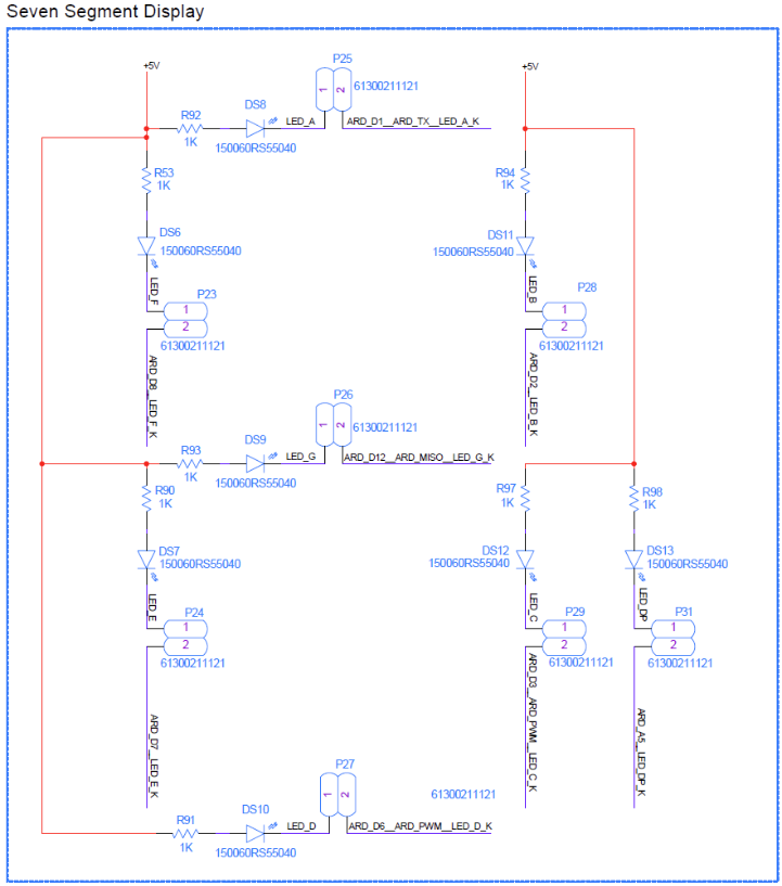
The AD-M2KCOMPEDU-EBZ is equipped with an SMD_LED 7-segment with decimal point (DP). The display uses common anodes connected to +5V and series resistors of 1kΩ. The cathodes are accessible at P23 to P31 2x8 pins header (bottom row).
On the top row of these headers, there are direct connections to the Arduino digital IO, thus placing jumpers to close these headers creates a quick link between the cathodes and Arduino outputs.
CAN transceiver
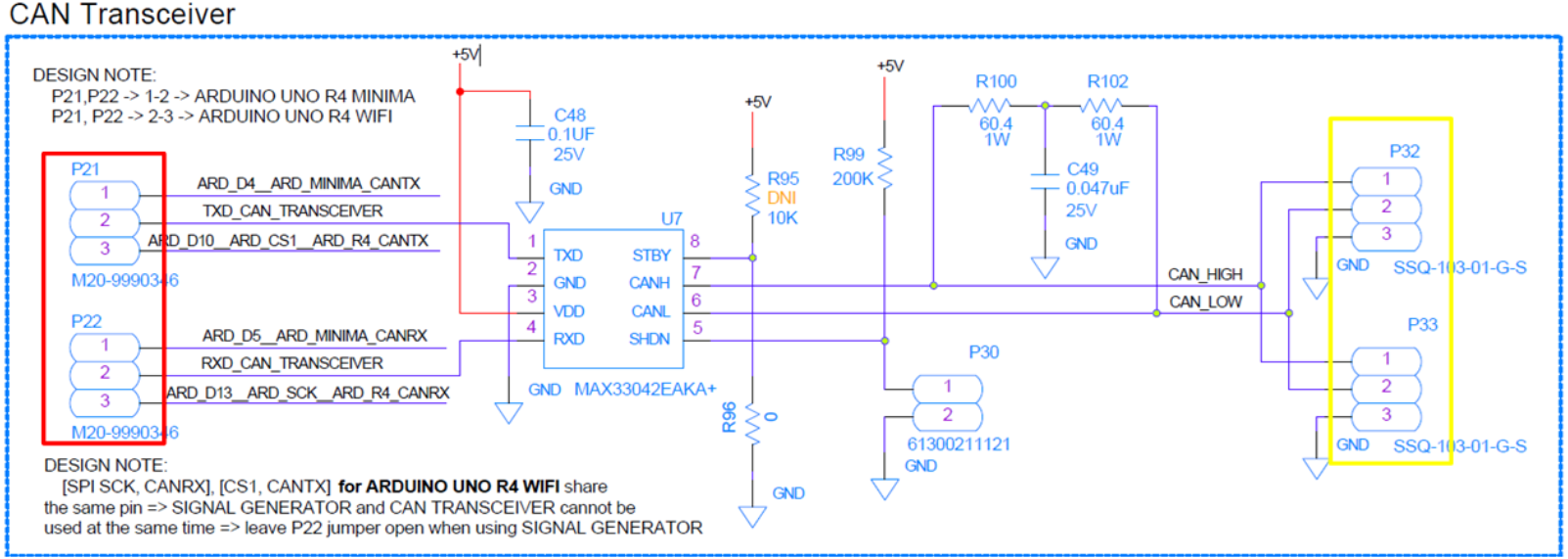
The AD-M2KCOMPEDU-EBZ contains a +5V CAN transceiver (MAX33042E) with integrated protection for industrial applications. This device has extended ±40V fault protection for equipment where overvoltage protection is required. It also incorporates high ±40kV ESD Human Body Model (HBM) protection and an input common-mode range (CMR) of ±25V.
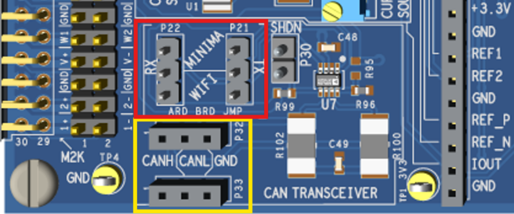
The data IO (RX/TX) of the transceiver are accessible via P21 and P22 3-pin headers that can also be configured as a quick-link to Arduino IO by using jumpers.
The transceiver connects to CAN-bus at the P32 and P33 female 3-pin headers that are pin-to-pin linked for chained connection.
The board also presents a 2x60Ω (120Ω) termination for the CAN-bus connection that is permanently connected.
Signal and PWM/CLK generator
Both the Signal and PWM/CLK generators are controlled from software, implemented on an Arduino R4 WiFi board, featuring an RA4M1 series microcontroller from Renesas, running on a 48MHz clock.
The software displays the Sig Gen or PWM/CLK menu to set the signal parameters on the MIDAS display screen via onboard Rotary Encoder.
Navigating in the menu is straightforward:
Rotate Left or Right: Change highlighted item in the menu or if an item is selected: Adjust the value of the selected item
Press: Select an item or change selection
Long Press: Exit to the upper-level menu
Onboard signal generator
The Sine/Triangle/Square wave signal generator is based on the AD9833 Programmable Waveform Generator with an SPI interface, using SS_AD9833 = Arduino Pin 10, controlled by the software on the Arduino R4 board.
At the AD9833 output, the C24 capacitor removes the DC component; afterwards the signal is sent through the R6-R39 divider, switchable by the ADG444 controlled switch, to the AD5443 Multiplying DAC (MDAC). Also both the ADG444 and the AD5443 are controlled by the software running on the Arduino R4 board: the ADG444 with a GPIO port (Arduino Pin 6), while the AD5443 with the SPI interface with SS_AD5433 = Arduino Pin 8.
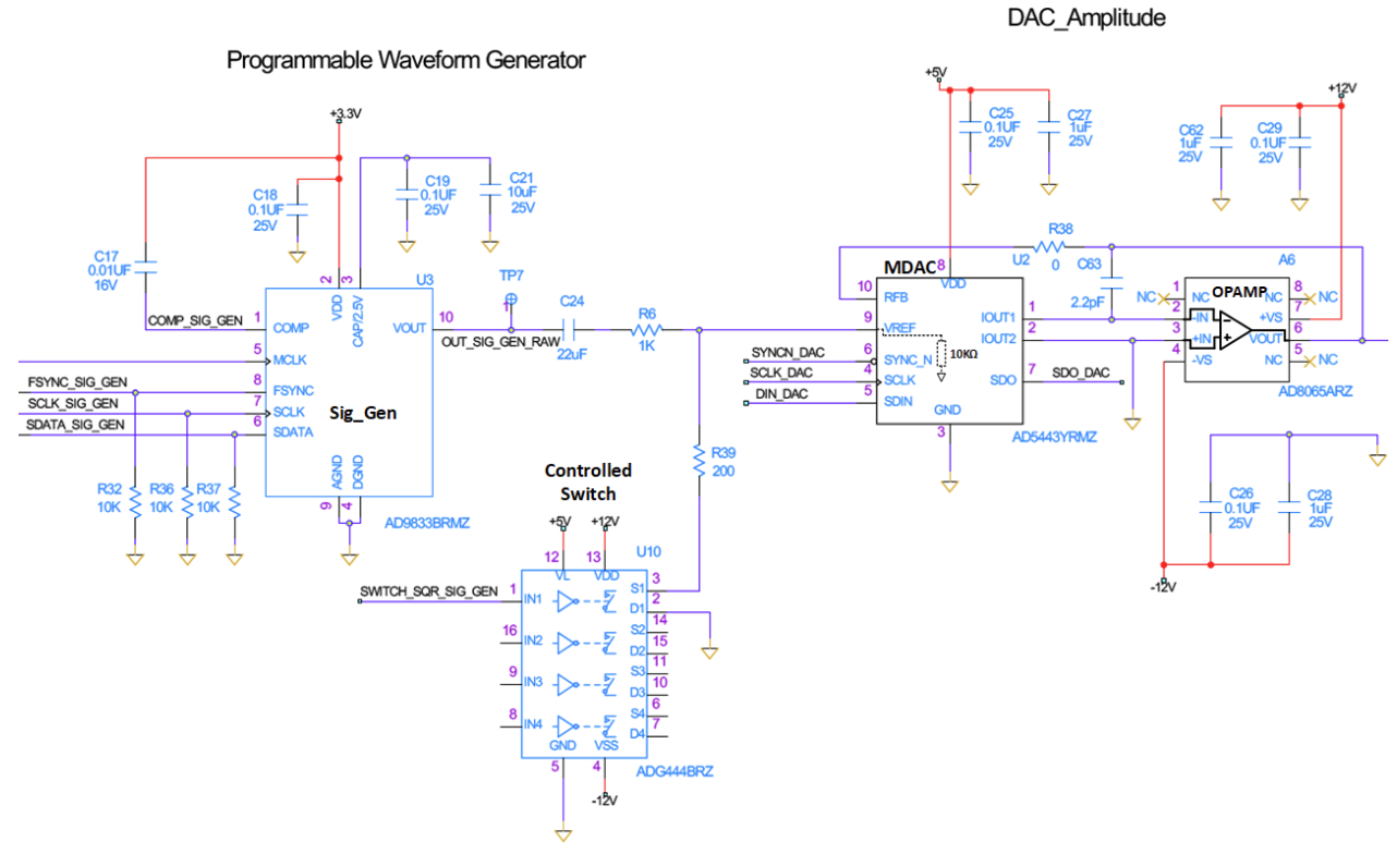
Figure 33 Signal Generator Sig_Gen, Controlled Switch, and MDAC Schematics
The AD5443 is a 12-bit current output, with an R-2R configuration, presenting a typical input equivalent resistance of 10kΩ.
When sine or triangle wave is generated by the AD9833, its nominal output amplitude is 600 mVpp. The ADG444 switch must be off, so this value is divided by the MDAC input resistance:
When square wave is generated by the AD9833, its nominal output amplitude is 3.3 Vpp. The ADG444 switch must be on, so this value is divided by R39 and the MDAC input resistance:
The output of the AD5443 DAC is converted to voltage by A6, an AD8065 op amp. Because the RFB feedback input also features a 10kΩ typical resistance, the output of the op amp will be equal to VREF divided by the DAC value:
where D is the DAC value, that is, the fractional representation of the digital word loaded to the DAC, D = 0…4095.
The output of A6 is followed by two stages, both implemented with an AD8066 op amp. The total gain of the two stages can be calculated as:
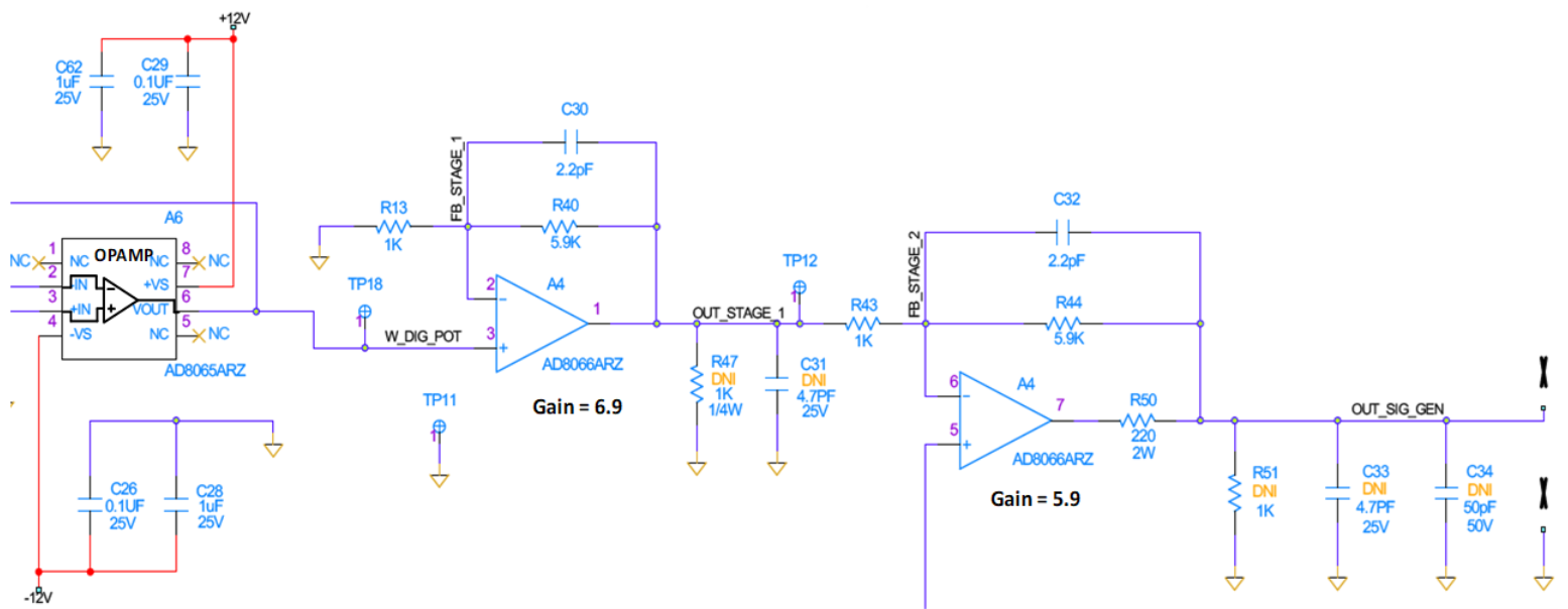
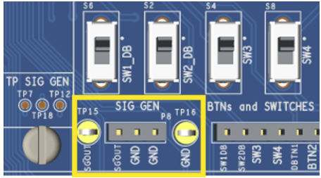
Although the gain is inverting, this does not change the signal generator behavior. The final amplifier output of the signal generator is accessible at the “SIG GEN” section at P8 and TP15, noted as “OUT_SG” on the silk screen.
The maximum output amplitude of the signal generator is, for sine and triangle wave:
and for the square wave:
Note that the output amplitude is limited by the software to maximum 20 VPP. If we express the output voltage in function of the D value sent to the AD5443 DAC, that is, express the number of volts per 1 LSB, we have the following nominal values:
For sine and triangle wave:
For square wave:
Note that these are nominal values and depend on many factors such as the AD9833’s real output voltage, the non-zero error, the monotony of the AD5443 DAC, and the resistor’s tolerances. The above values are set by constants in the software application and can be adjusted in the calibration menu.
The Sig Gen output is protected against short circuit damage by means of a 220Ω / 2W (R50) output series resistor that is included in the negative feedback loop. Thus, the output impedance of the Sig Gen is <1Ω up to 54mA load currents (12V/220Ω).
The absolute maximum output swing is dependent on the loading current such that:
This includes both the offset and amplitude.
Example: For a 50Ω standard Load, the max/min output level can be calculated as:
Setting the amplitude above this value determines the AD8066 operational amplifier output to saturate, thus truncated waveforms are achieved at the Sig_Gen output.
The Sig_Gen output can also be driven into saturation with HiZ loads if the sum of amplitude and offset settings exceeds the ±12V supply rail. The Sig_Gen parameters settings menu does not limit the user to enter values that will saturate the Sig_Gen output, precisely for educational purposes. In this way truncated waveforms can be obtained.
Note
The AD-M2KCOMPEDU-EBZ Sig_Gen has a bandwidth limitation of 2MHz, however, setting the frequency higher than 400kHz will result in attenuated amplitude versus the set amplitude. The expected Sine amplitude attenuation for a specific frequency can be estimated considering the frequency characteristic that presents a -20dB/decade slope past the cutoff frequency of @400kHz.
While for the square wave, the bandwidth limitation impacts the rise/fall edge rates first @200kHz and only later the amplitude.
Onboard signal generator’s DC offset
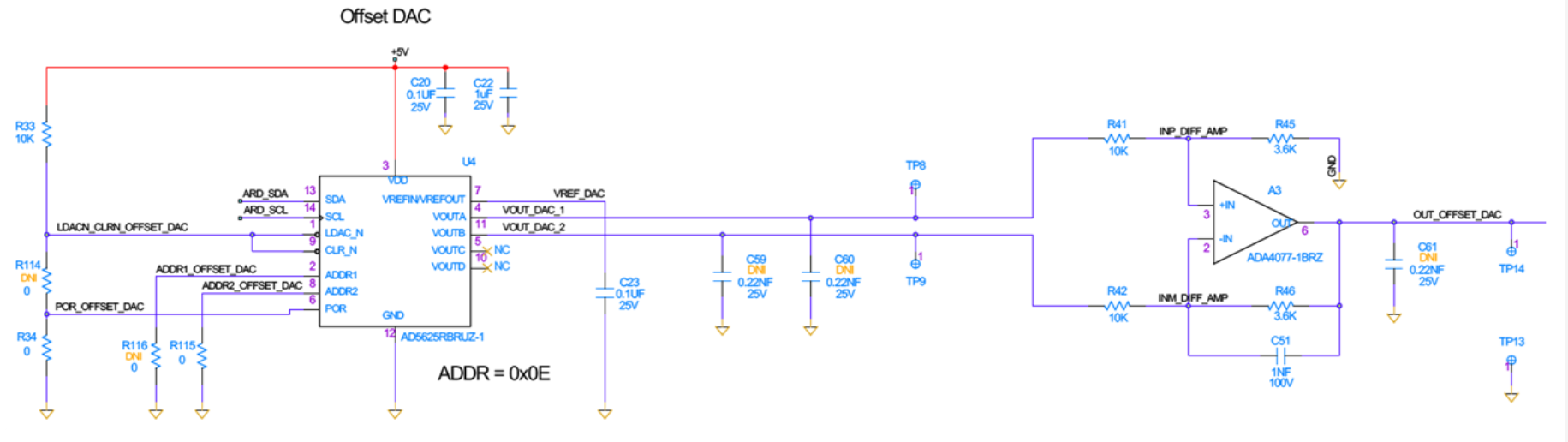
The DC offset of the signal generator is provided by the AD5625R 12-bit quad DAC, controlled by the I2C protocol. Two of the DAC outputs are fed to the one op amp differential amplifier implemented by the ADA4077-1.
The output voltage at the differential amplifier can be expressed as:
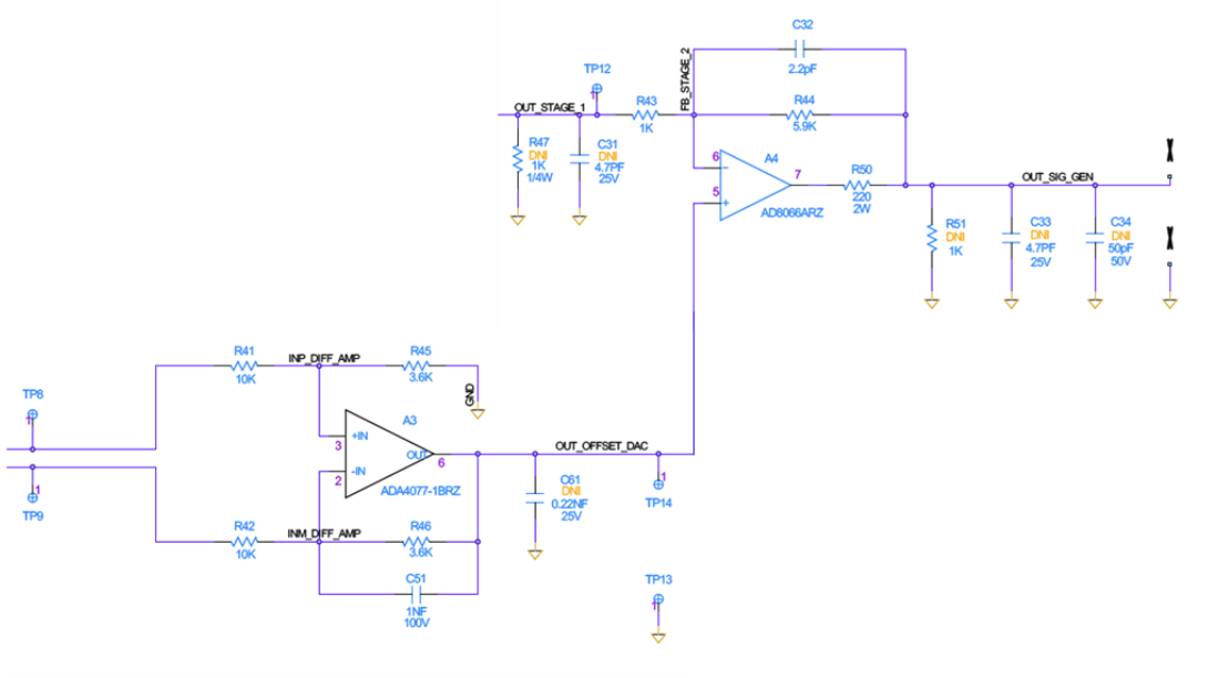
The differential amplifier’s output is connected to the noninverting input of the output stage. As the maximum value of \((V_VOUT_DAC_1 - V_VOUT_DAC_2)\) is ±5V, it follows that the maximum DC output voltage of the signal generator is:
Note that the output offset voltage is limited by software to ±10V. Also note that the signal generator menu allows stopping the AD9833 wave output (waveform: OFF) and adjusting the DC offset to a nonzero value. In this way, the signal generator can be used as a third DC reference voltage.
Expressing the signal generator’s DC output in terms of V per LSB, results:
Like the signal generator amplitude V/LSB values, this is a nominal value and can also slightly differ in the real circuit. However, due to the AD5625R’s internal precision voltage reference and the 1% tolerance resistances used in the gain stages, this value is not adjusted in software during calibration. Instead, the calibration procedure adjusts the Signal Generator’s initial offset to 0 as close as possible.
PWM/CLK generator
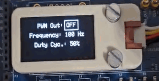
The PWM/Clock signal generator is implemented by the RA4M1 microcontroller’s Timer peripheral, connected to a PWM output (pin D9/PWM on the Arduino R4). Frequency and Duty cycle can be set in PWM/CLK operating mode interface of the signal generator menu.
Note that both the signal generator and the PWM/CLK generator can run independently, set from the generator menu.
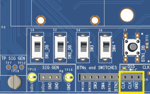
The output of the PWM generator is then buffered using two HEX inverters, providing the 5V-TTL clock and an inverted version of the Clock signal: CLK/PWM and \(\overline{CLK}\)/\(\overline{PWM}\). The two clock signals are accessible at TP17 and TP21 and connector P14 pin 7 and 8.
Furthermore, the CLK real-time state can be monitored with the dedicated LED DS5 that lights up green when PWM/CLK outputs state is logic ‘1’ up to 20Hz. For higher frequency (larger than about 25Hz), the PWM output can be used to modulate the brightness of the DS5 LED.
Display
The AD-M2KCOMPEDU-EBZ includes a MIDAS MDOB128064V2V-Y graphic OLED monochrome display, 128 x 64 Pixels, accessible via I2C. This display is directly connected to the Arduino plugin header at P4/9,10 (SDA, SCL). Two pull up 10kΩ resistors (R8, R9) are placed on the board for the SDA and SCL I2C bus. Note that the I2C address is 0x3C.
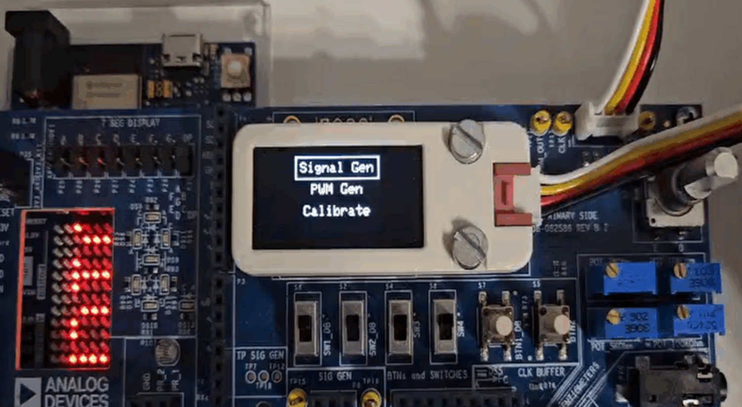

Menu - User Interface
Calibration procedure interface (Sig Gen offset and amplitude)
Operating modes interface
Operating modes interface:
Sig_Gen and PWM/CLK generator
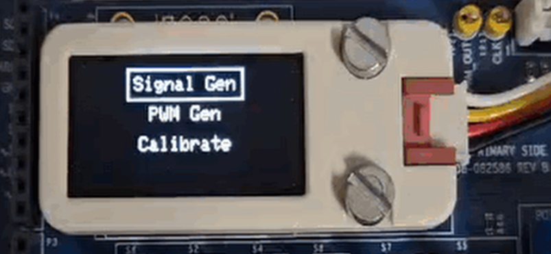
The Sig_Gen menu is accessible using a rotary encoder with push-to-click functionality. The selection is highlighted by a borderline around the target parameters. A click on the rotary encoder allows the user to edit the selected parameter. After the edit is done, a second click on the rotary encoder will jump back to the parameters list.
The Sig Gen and PWM/CLK menu includes access to following parameters:
Waveform type: Off/Sine/Triangle/Square/PWM/CLK.
Peak to peak amplitude: In the range of [100mV to 20V], 100mV steps.
Frequency: In the range of [10Hz to 2MHz] ([1Hz to 2MHz] for PWM).
DC offset: In the range of [-10V +10V], 100mV steps.
PWM/CLK duty cycle: In the range of [1% to 99%]
The peak-to-peak amplitude and offset settings are available only for the Sinus, Triangle, and Square waveforms, while the PWM/CLK signals are 5V TTL routed on separated output pins. See PWM/CLK generator section.
The edited Sig_Gen parameters are updated instantaneously, no click to confirm is required.
Offset DAC as Programmable Supply Rail / Audio DSP
The AD5625RBRUZ-1 DAC in conjunction with Arduino can be programmed to work as a custom waveform generator OR an audio DSP. The onboard signal generator can be set to deliver a 0V DC level at OUT_STAGE1, thus enabling the user to experiment with the DAC via I2C, and routing the amplified signal to the Sig_Gen output that can be further routed to the audio amplifier such that the result can be heard via headphones or speaker.