Evaluating the AD7175-2
Features
Evaluation Kit Contents
EVAL-AD7175-2SDZ evaluation board
Evaluation software CD
7 V to 9 V ac-to-dc adapter
Equipment Needed
DC signal source
PC running Windows XP to Windows 7
General Description
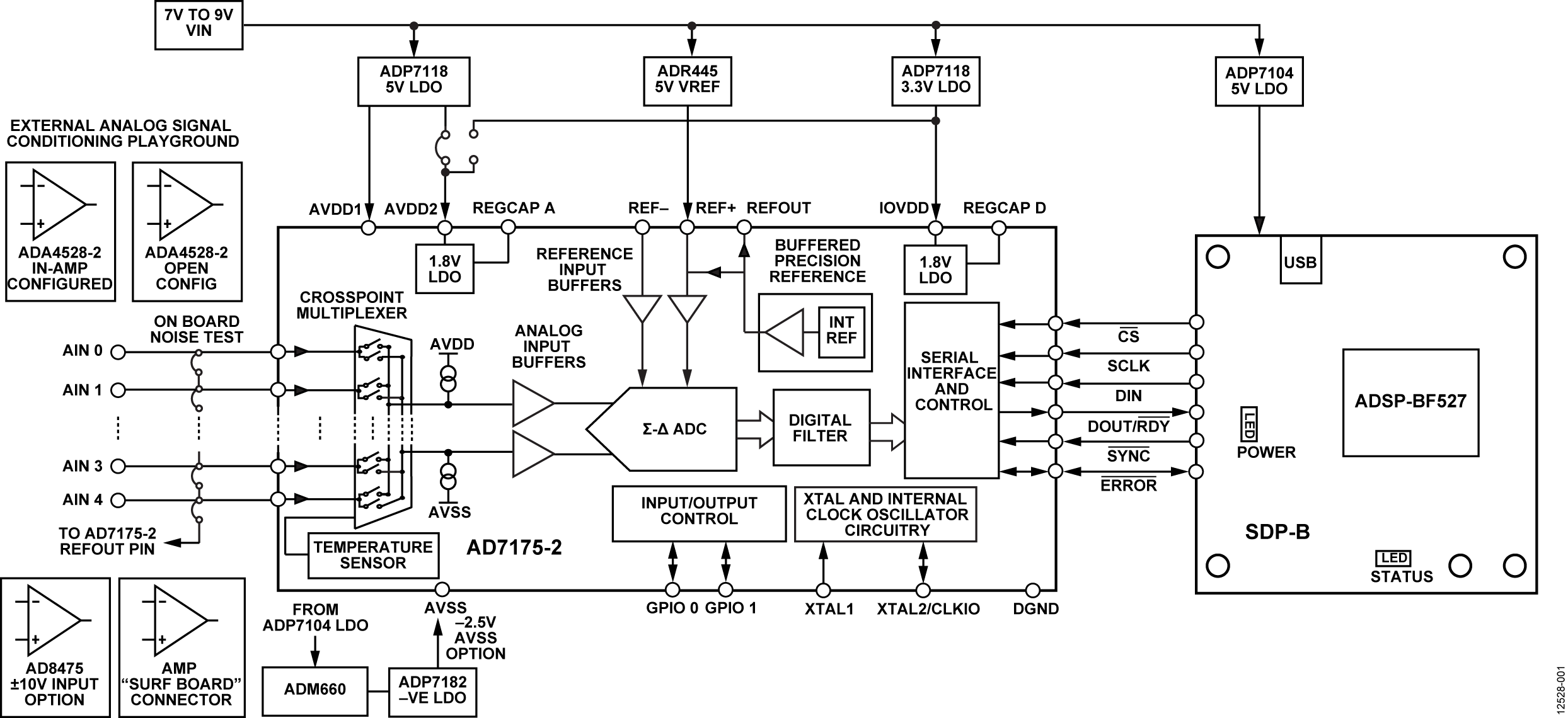
The EVAL-AD7175-2SDZ evaluation kit features the AD7175-2, a 24-bit, 250 kSPS analog-to-digital converter (ADC) with integrated rail-to-rail analog input buffers, on-board power supply regulation, and an external amplifier section for amplifier evaluation. A 7 V to 9 V ac-to-dc adapter is regulated to 5 V and 3.3 V, which supply the AD7175-2 and support components. The EVAL-AD7175-2SDZ evaluation board connects to the USB port of a PC via the SDP-B controller board.
The AD7175-2 Eval+ software fully configures the AD7175-2 device functionality via an interactive block diagram and a user accessible register interface, and provides DC time domain analysis in the form of waveform graphs, histograms, and associated noise analysis for ADC performance evaluation.
Full specifications for the AD7175-2 are available in the product data sheet, which should be consulted in conjunction with this user guide when using the evaluation board.
Functional Block Diagram
Quick Start Guide
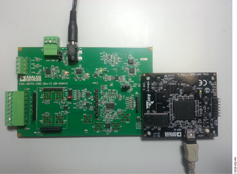
Follow these steps to set up the evaluation board:
Disconnect the SDP-B board from the USB port of the PC. Install the AD7175-2 Eval+ software from the enclosed CD. Restart the PC after installation.
Connect the SDP-B board to the evaluation board.
Fasten the two boards together with the enclosed plastic screw washer set.
Connect the external 9 V power supply to Connector J5 of the evaluation board. Set Link LK2 to Position B.
Connect the SDP-B board to the PC via the USB cable. For Windows XP, you may need to search for the SDP-B drivers. Choose to automatically search for the drivers for the SDP-B board if prompted by the operating system.
Launch the AD7175-2 Eval+ software from the Analog Devices subfolder in the Programs menu.
Quick Start Noise Test
Insert Link LK8 to Link LK12 to initiate the noise performance test mode. In this mode, analog input channels short to the REFOUT pin.
Click Start Sampling to acquire samples from the ADC.
The Samples numeric control in the top right corner of the main window sets the number of samples collected in each batch.
Evaluation Board Hardware
Device Description
The AD7175-2 is a highly accurate, high resolution, multiplexed, 2-/4-channel (fully differential/single-ended) Σ-Δ ADC. The AD7175-2 has a maximum channel-to-channel scan rate of 50 kSPS (20 µs) for fully settled data. The output data rates range from 5 SPS to 250 kSPS. The device includes integrated rail-to-rail analog input and reference input buffers, an integrated precision 2.5 V reference, and an integrated oscillator.
See the AD7175-2 data sheet for complete specifications. Consult the data sheet in conjunction with this user guide when using the evaluation board. Full details for the SDP-B are available at the SDP-B product page on the Analog Devices website.
Hardware Link Options
By default, the evaluation board is configured to operate from the supplied 9 V ac-to-dc adapter connected to connector J5. The 5 V supply required for the AD7175-2 comes from the ADP7118 on-board low dropout regulator (LDO). The ADP7118, with a 5 V output voltage, receives its input voltage from J3 or J5 (depending on the position of LK2) and generates a 5 V output.
Link |
Default Option |
Description |
|---|---|---|
LK1 |
A |
Selects the voltage applied to the power supply sequencer circuit (U3); dependent on AVDD1. Place in Position A if using 5 V AVDD1, or Position B if using 2.5 V AVDD1. |
LK2 |
B |
Selects the external power supply from Connector J3 (Position A) or Connector J5 (Position B). |
LK3 to LK7 |
Not Inserted |
Inserting these links sets up the on-board noise test prior to SL8 to SL11 to allow the inputs to the on-board amplifiers, U8 and U9, to be shorted. In this mode, all inputs short to REFOUT. |
LK8 to LK12 |
Inserted |
Inserting these links sets up the on-board noise test close to the ADC analog inputs. In this mode, all inputs short to REFOUT. |
SL1 |
A |
Sets the voltage applied to the AVDD2 pin. Operates using the AVDD1 supply (default). Position B sets the AVDD2 voltage to 3.3 V supply from the ADP7118 (3.3 V) (U10) regulator. |
SL2 |
A |
Selects between an external or on-board AVDD1 source. Supplies AVDD1 from the ADP7118 (5 V) (U7) (default). |
SL3 |
A |
Selects between an external or on-board AVSS source. Supplies AVSS from the ADP7182 (−2.5 V) (U4) (default). |
SL4 |
A |
Connects AIN4 to: A4/J6 (Position A), REFOUT pin on the AD7175-2 (Position B), or AVSS (Position C). Position B and Position C are used to simplify using a single-ended input source. |
SL5 |
B |
Selects between an external or on-board IOVDD source. Supplies IOVDD from the ADP7118 (3.3 V) (U10) (default). The evaluation board operates with 3.3 V logic. |
SL8 |
A |
Routes A0 to: AIN0 pin on the AD7175-2 (Position A), Buffer/In-amp U8 (Position B), Funnel Amp U9 with gain of 0.8× (Position C), or J10-1 (Position D). |
SL9 |
A |
Routes A2 to: AIN2 pin on the AD7175-2 (Position A), Buffer U12 (Position B), or Funnel Amp U9 gain of 0.4× (Position C). |
SL10 |
A |
Routes A3 to: AIN3 pin on the AD7175-2 (Position A), Buffer U12 (Position B), or Funnel Amp U9 gain of 0.4× (Position C). |
SL11 |
A |
Routes A1 to: AIN1 pin on the AD7175-2 (Position A), Buffer/In-amp U8 (Position B), Funnel Amp U9 with gain of 0.8× (Position C), or J10-7 (Position D). |
G16 |
Inserted |
Sets the on-board In-amp U8 to a gain of 16. Only one of G16, G32, G64, and G128 should be inserted at a time. |
G32 |
Not Inserted |
Sets the on-board In-amp U8 to a gain of 32. Only one of G16, G32, G64, and G128 should be inserted at a time. |
G64 |
Not Inserted |
Sets the on-board In-amp U8 to a gain of 64. Only one of G16, G32, G64, and G128 should be inserted at a time. |
G128 |
Not Inserted |
Sets the on-board In-amp U8 to a gain of 128. Only one of G16, G32, G64, and G128 should be inserted at a time. |
R49 to R51 |
Inserted |
Connects AVSS and AGND for single-supply operation. To operate in split supply mode, remove these links. |
Sockets and Connectors
Connector |
Function |
Connector Type |
Manufacturer |
Manufacturer Number |
|---|---|---|---|---|
J1 |
Connector to the SDP-B |
120-way connector, 0.6 mm pitch |
Hirose |
FX8-120S-SV(21) |
J2 |
External MCLK Input |
Straight PCB mount SMB/SMA jack |
Tyco |
1-1337482-0 |
J3 |
External bench top voltage supply for the EVAL-AD7175-2SDZ |
Power socket block, 3-pin, 3.81 mm pitch |
Phoenix Contact |
MC 1,5/ 3-G-3,81 |
J5 |
External ac-to-dc adapter input for the EVAL-AD7175-2SDZ, 7 V to 9 V |
DC power connectors, 2 mm SMT power jack |
Kycon |
KLDX-SMT2-0202-A |
J6 |
Analog input terminal block; wired connection to external source or sensor |
Power socket block, 8-pin, 3.81 mm pitch |
Phoenix Contact |
MC 1,5/ 8-G-3,81 |
J9 |
External bench top voltage supply option for AVDD1/AVDD2, IOVDD, and AVSS inputs on the AD7175-2 |
Screw terminal block, 3.81 mm pitch |
Phoenix Contact |
MKDS 1/4-3.81 |
J10 |
Optional header |
7-way, 2.54 mm pin header |
Samtec |
SSW-107-01-T-S |
J13 |
Optional header |
7-way, 2.54 mm socket |
Samtec |
TLW-107-05-G-S |
A0 to A4 |
Analog inputs to ADC |
Straight PCB mount SMB/SMA jack |
Tyco |
1-1337482-0 |
A7 |
PMOD-compatible header |
6-pin SIL header (0.1” pitch) |
Harwin |
20-9990646 |
Serial Interface
The EVAL-AD7175-2SDZ evaluation board connects via the serial peripheral interface (SPI) to the Blackfin® ADSP-BF527 on the SDP-B. There are four primary signals: CS, SCLK, and DIN (all inputs), and one output from the ADC, DOUT/RDY. To operate the evaluation board in standalone mode, disconnect the evaluation board from the SDP-B controller board. Use the test points to connect the signals to an alternative digital capture setup or the PMOD-compatible header (A7).
Power Supplies
Power the evaluation board from the ac-to-dc adapter connected to J5, or from an external bench top supply applied to J3 or J9. Linear LDOs generate the required voltages from the applied input voltage (VIN) rail when using J3 or J5. Use J9 to bypass the on-board regulators. An ADP7118 regulator generates the 5 V (single supply) and 2.5 V (split supply) supplies for the AVDD1 and AVDD2 rails to the ADC; a second ADP7118 generates 3.3 V for the IOVDD rail. The ADP7104 supplies 5 V for the SDP-B controller board as well as 5 V for the ADM660 voltage converter to generate −5 V to supply the ADP7182. The ADP7182 generates the −2.5 V supply for AVSS when operating in split supply mode. Each supply is decoupled where it enters the board and again at each device in accordance with the schematic.
Configuration |
Input Voltage Range |
Description |
|---|---|---|
Single Supply (Regulated) |
7 V to 9 V |
The 7 V to 9 V input is regulated to 5 V for AVDD1/AVDD2 and 3.3 V for IOVDD. This also powers the external 5 V reference. |
Single Supply (Unregulated) |
7 V to 9 V, 5 V, and 3.3 V |
The input is unregulated and connects directly to AVDD1/AVDD2 and IOVDD from J5. The 7 V to 9 V input powers the external 5 V reference. |
Split Supply (Regulated) |
7 V to 9 V |
The 7 V to 9 V input is regulated to 2.5 V for AVDD1/AVDD2, −2.5 V for AVSS and 3.3 V for IOVDD. The 7 V to 9 V input powers the external 5 V reference. |
Split Supply (Unregulated) |
7 V to 9 V, ±2.5 V, and 3.3 V |
The input is unregulated and connects directly to AVDD1/AVDD2 and IOVDD from J5. The 7 V to 9 V input powers the external 5 V reference. |
Power Supply Configurations
Single Supply (Regulated)
There are two available power supply options for the single supply (regulated) configuration:
An ac-to-dc adapter (included) connected to J5. Set LK2 to Position B.
A bench top power supply connected to J3. Set LK2 to Position A, and ensure that AVSS = AGND = 0 V.
Set all other links and solder links to the default settings as outlined in Table 1.
Single Supply (Unregulated)
Move SL2 to Position B and SL5 to Position A.
Connect the two terminals of J9 labeled AGND and AVSS.
Connect 0 V (GND) to J9 at the terminal labeled AGND.
Connect 5 V to J9 at the terminal labeled AVDD.
Connect 3.3 V to J9 at the terminal labeled IOVDD.
Connect the 7 V to 9 V input to J5.
Set all other links and solder links to the default settings as outlined in Table 1.
Split Supply (Regulated)
Remove R49 to R51. These links connect AVSS to AGND.
Insert a 0 Ω resistor for R85.
Set LK1 to Position B, which sets the input to the power monitor circuitry to work with the lower AVDD1 supply of 2.5 V.
Connect a bench top power supply to J5 and set LK2 to Position B.
Set all other links and solder links to the default settings as outlined in Table 1.
Split Supply (Unregulated)
Move SL2 and SL3 to Position B and SL5 to Position A.
Remove R49 to R51.
Connect 0 V (GND) to J9 at the terminal labeled AGND.
Connect 2.5 V to J9 at the terminal labeled AVDD.
Connect −2.5 V to J9 at the terminal labeled AVSS.
Connect 3.3 V to J9 at the terminal labeled IOVDD.
Connect 7 V to 9 V to J5.
Set LK1 to Position B. This sets the input to the power monitor circuitry to work with the lower AVDD1 supply of 2.5 V.
Set all other links and solder links to the default settings as outlined in Table 1.
Analog Inputs
The primary analog inputs of the EVAL-AD7175-2SDZ evaluation board can be applied in two ways:
J6 connector on the left side of the board
A0 to A4 SMB/SMA footprints on the evaluation board
The analog inputs route directly to the associated analog input pins on the AD7175-2, provided that the LK5 to LK9 links (on-board noise test) are removed. The AD7175-2 Eval+ software is set up to analyze DC inputs to the ADC. The AD7175-2 input buffers work for DC input signals.
Reference Options
The EVAL-AD7175-2SDZ evaluation board includes an external 5 V reference, the ADR445. The AD7175-2 includes an internal 2.5 V reference. The default operation is to use the external reference input, which is set to accept the 5 V ADR445 on the evaluation board.
Evaluation Board Software
Software Installation
The EVAL-AD7175-2SDZ evaluation kit includes software on a CD.
Double-click the setup.exe file from the CD to run the installer. The
default installation location for the software is
C:\Program Files\Analog Devices\AD7175-2 Eval+\.
Important
Install the Eval+ software before connecting the evaluation board and SDP-B board to the USB port of the PC to ensure that the evaluation system is correctly recognized when connected to the PC.
There are two parts to the installation:
Proceed through all installation steps to place the software and drivers in the appropriate locations. Connect the SDP-B board to the PC only after the software and drivers are installed. The installer may prompt you to allow the program to make changes to the computer. Click Yes to proceed.
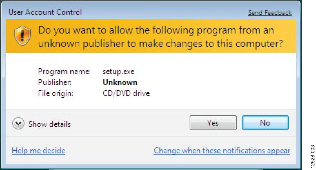
You may receive a security warning as part of the SDP-B controller board driver installation. Click Install to proceed. Without this confirmation, the software cannot operate correctly.
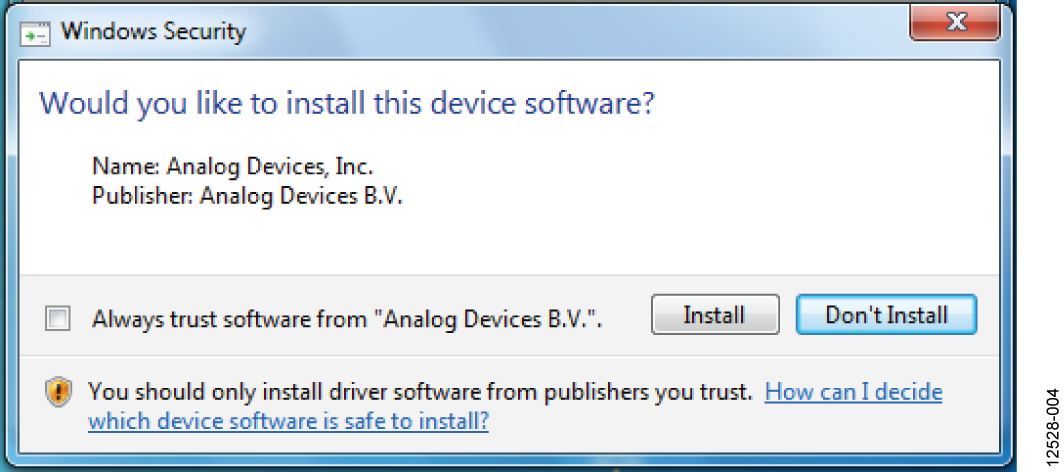
After installation is complete, connect the evaluation board to the SDP-B board, then connect via USB to the computer. Follow these steps to verify that the SDP-B controller board driver is installed and working correctly:
Allow the Found New Hardware Wizard to run.
When the drivers are installed, check that the board has connected correctly by looking at the Device Manager of the PC. The Device Manager can be found by right-clicking My Computer, selecting Manage, then Device Manager from the list of System Tools.
The SDP-B board appears under ADI Development Tools as Analog Devices System Development Platform or similar. The installation is complete.
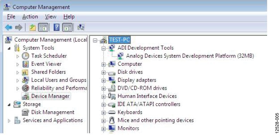
Launching the Software
The Eval+ software can be launched when the evaluation board and SDP-B board are correctly connected to the PC. The Eval+ software can also be operated without hardware.
From the Start menu, click Programs > Analog Devices > AD7175-2 Eval+. The main window of the Eval+ software displays.
If the AD7175-2 evaluation system is not connected to the USB port via the SDP-B when the software is launched, the Select Interface… dialog box appears. Connect the evaluation board to the USB port of the PC, wait a few seconds, then click the green arrows to rescan the USB ports. When connected, click Work Online to proceed. Click Work Offline to use the software without hardware.
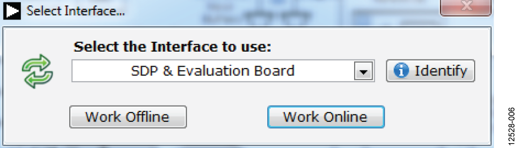
Software Operation
Overview of the Main Window
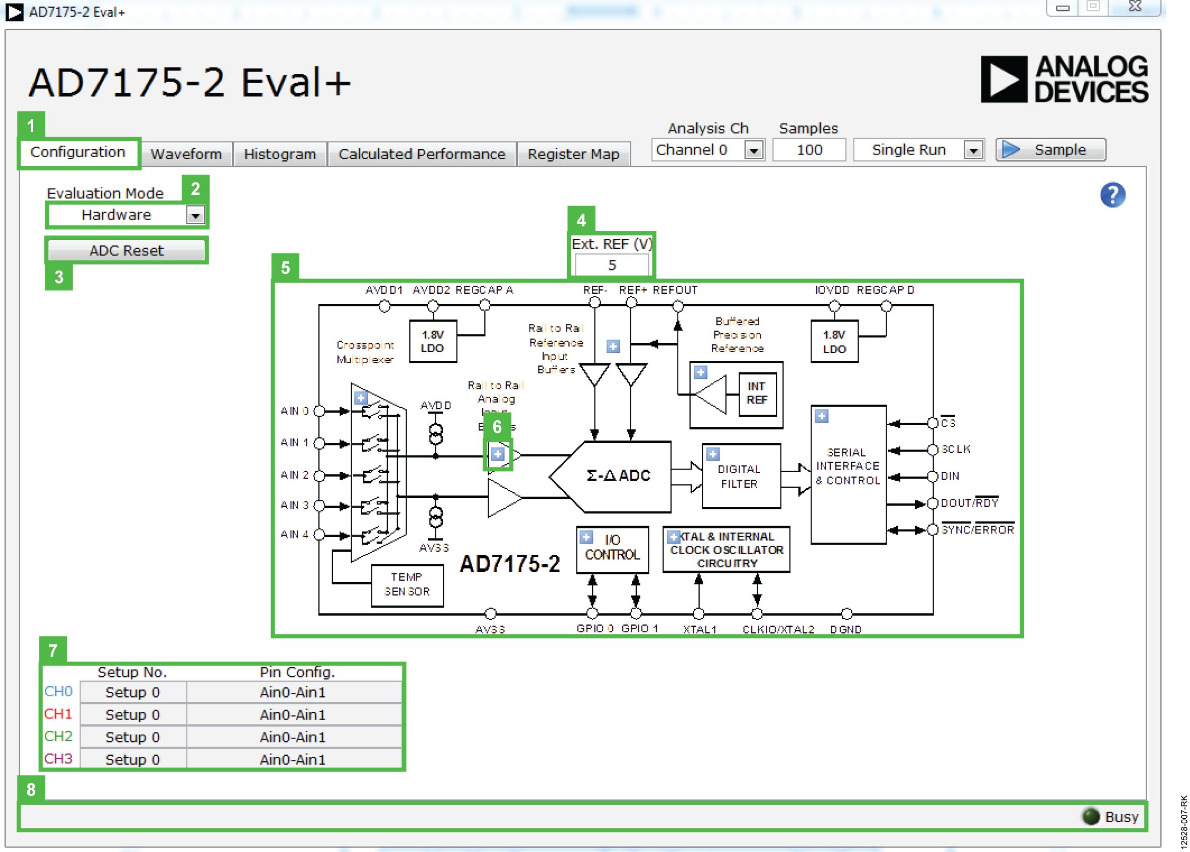
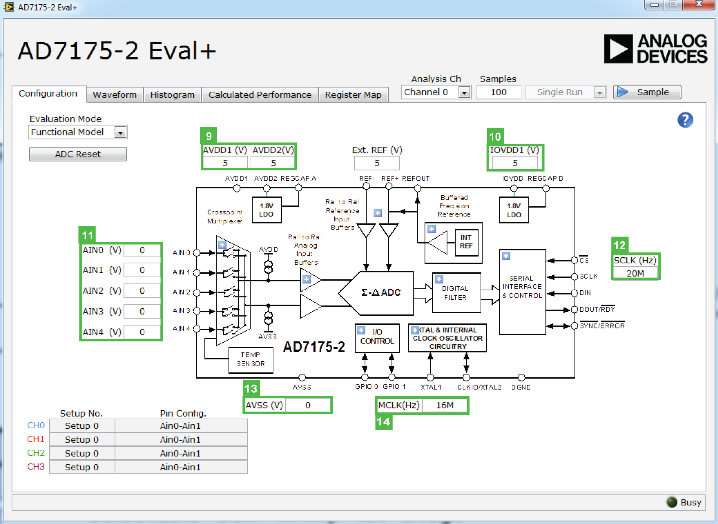
The main window displays the significant control buttons and analysis indicators of the AD7175-2 Eval+ software. The main window is divided into five tabs: Configuration, Waveform, Histogram, Calculated Performance, and Register Map.
Configuration Tab
Evaluation Mode (2)
Click here to select the evaluation mode. Selecting Hardware evaluation mode uses the EVAL-AD7175-2SDZ board to evaluate the ADC. Selecting Functional Model evaluation mode uses a model of the ADC for evaluation.
ADC Reset (3)
Click ADC Reset to perform a software reset of the AD7175-2. There is no hardware reset pin. Perform a hard reset by removing power to the board. The software reset has the same effect as a hard reset.
Ext. REF (4)
The Ext. REF field sets the external reference voltage used for calculating the results on the waveform and histogram tabs. The evaluation board has an external 5 V ADR445 reference, which can be bypassed; change the external reference voltage value in Ext. REF to ensure correct calculation of results in the Waveform and Histogram tabs.
Functional Block Diagram (5)
The functional block diagram of the ADC shows each of the separate functional blocks within the ADC. Clicking a configuration button on this graph opens the configuration popup window for that block. Not all blocks have a configuration button.
Configuration Popup Button (6)
Each configuration popup button opens a different window allowing for configuration of the relevant functional block.
Channel Configuration Overview (7)
This section shows the channel configuration, including setup and analog inputs, and allows a quick check of how the ADC is set up.
Status Bar (8)
The status bar displays status updates such as Analysis Completed and Reset Completed during software use, as well as the software version and busy indicator.
Analog Supply Voltage (9 & 13)
Sets the analog supply voltages used in the functional model for checking power supply limits and calculating the power dissipation figures. These controls are only visible when Functional Model evaluation mode is enabled.
Digital Supply Voltage (10)
Sets the digital supply voltage used in the functional model for checking power supply limits and calculating the power dissipation figures. Only visible when Functional Model evaluation mode is enabled.
Analog Input Voltage (11)
Sets the analog input voltages used in the functional model for calculating the ADC output codes. The voltages set on these controls are DC only with no noise. Only visible when Functional Model evaluation mode is enabled.
External SCLK Frequency (12)
Sets the external SCLK frequency for the SPI interface. This value is used in the functional model to determine if the SCLK frequency is within the permitted range. Only visible when Functional Model evaluation mode is enabled.
External MCLK Frequency (14)
Sets the external MCLK frequency to be used when an external clock source is selected by the ADC in the functional model. Only visible when Functional Model evaluation mode is enabled.
Waveform Tab
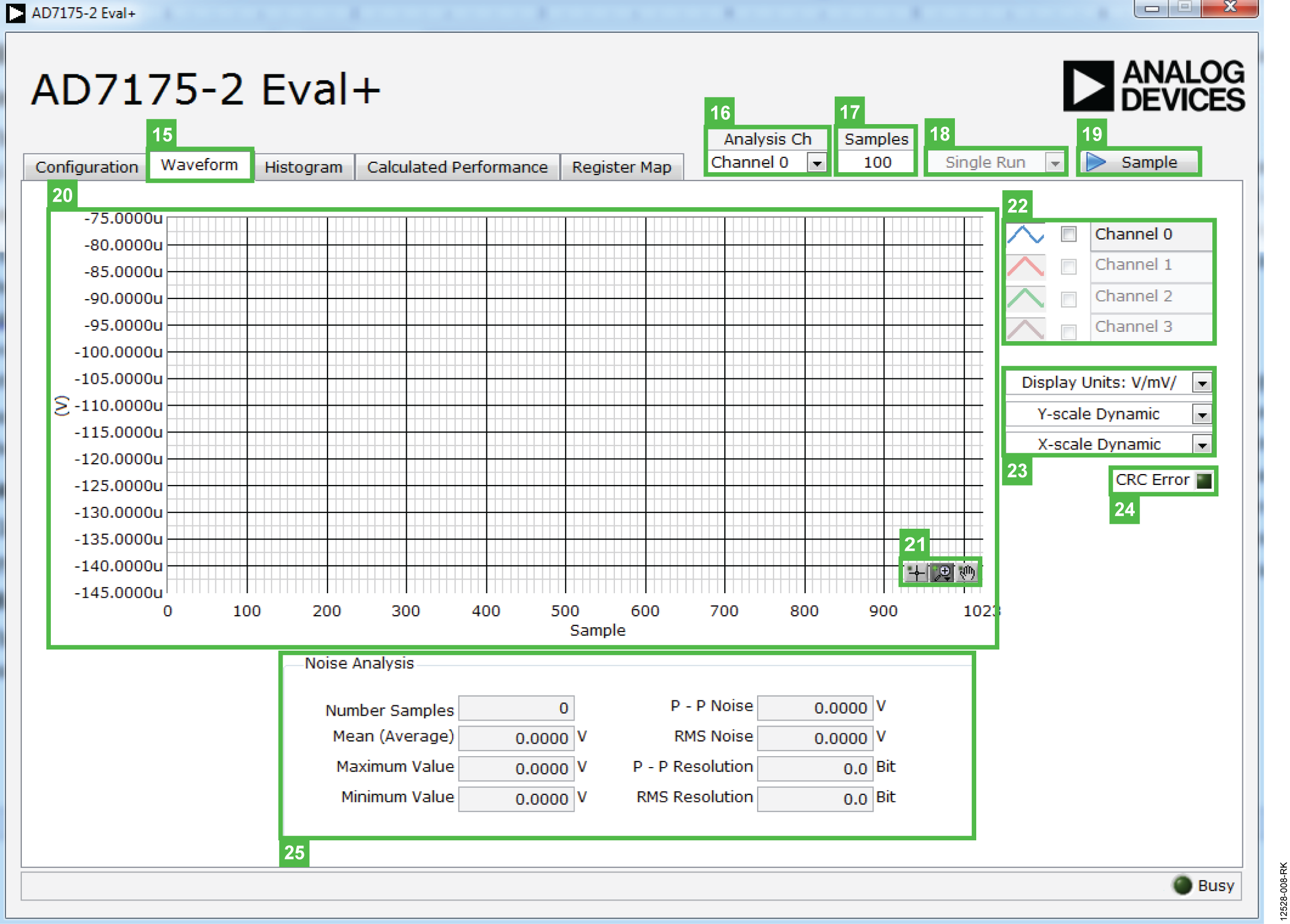
Analysis Channel (16)
The Noise Analysis section and histogram graph show the analysis of the channel selected via the Analysis Channel control.
Samples (17 and 18)
The Samples numeric control (17) and batch control (18) set the number of samples gathered per batch and whether a single batch or multiple batches of samples are gathered. You can capture a defined sample set or continuously gather batches of samples.
Sample (19)
Click the Sample button to start gathering ADC results. Results appear in the waveform graph (20).
Waveform Graph and Controls (20 and 21)
The data waveform shows each successive sample of the ADC output. Zoom in on the data using the control toolbar (21). Change the scales on the graph by typing values into the x-axis and y-axis fields.
Channel Selection (22)
This control chooses which channels display on the data waveform, and also shows the analog inputs for each channel. These controls only affect the display and have no effect on the channel settings in the ADC register map.
Display Units and Axis Controls (23)
Click Display Units to select whether the data graph displays in voltages or codes. The axis controls can be switched between dynamic and fixed. When dynamic is selected, the axis automatically adjusts after each batch of samples. When fixed is selected, the user can program the axis ranges manually.
CRC Error (24)
This LED indicator illuminates when a cyclic redundancy check (CRC) error is detected in the communications between the software and the AD7175-2. The CRC functionality on the AD7175-2 is disabled by default and must be enabled for this indicator to work.
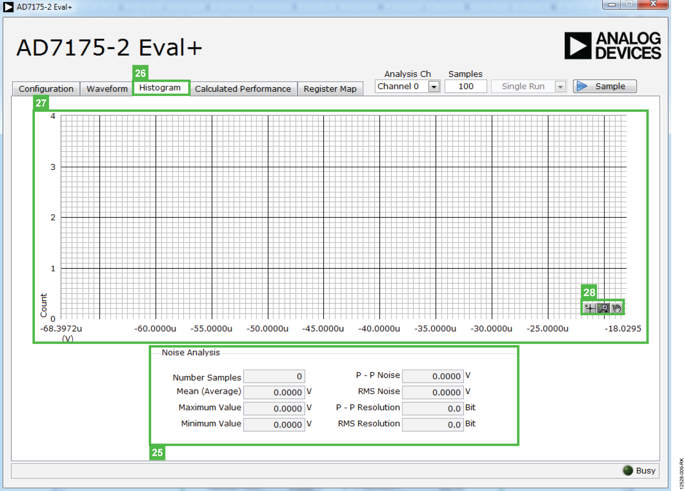
Noise Analysis (25)
The Noise Analysis section displays the results of the noise analysis for the selected analysis channel, including both noise and resolution measurements.
Histogram Tab
Histogram Graph and Controls (27 and 28)
The data histogram shows the number of times each sample of the ADC output occurs. Zoom in on the data using the control toolbar (28). Change the scales on the graph by typing values into the x-axis and y-axis fields.
Calculated Performance Tab
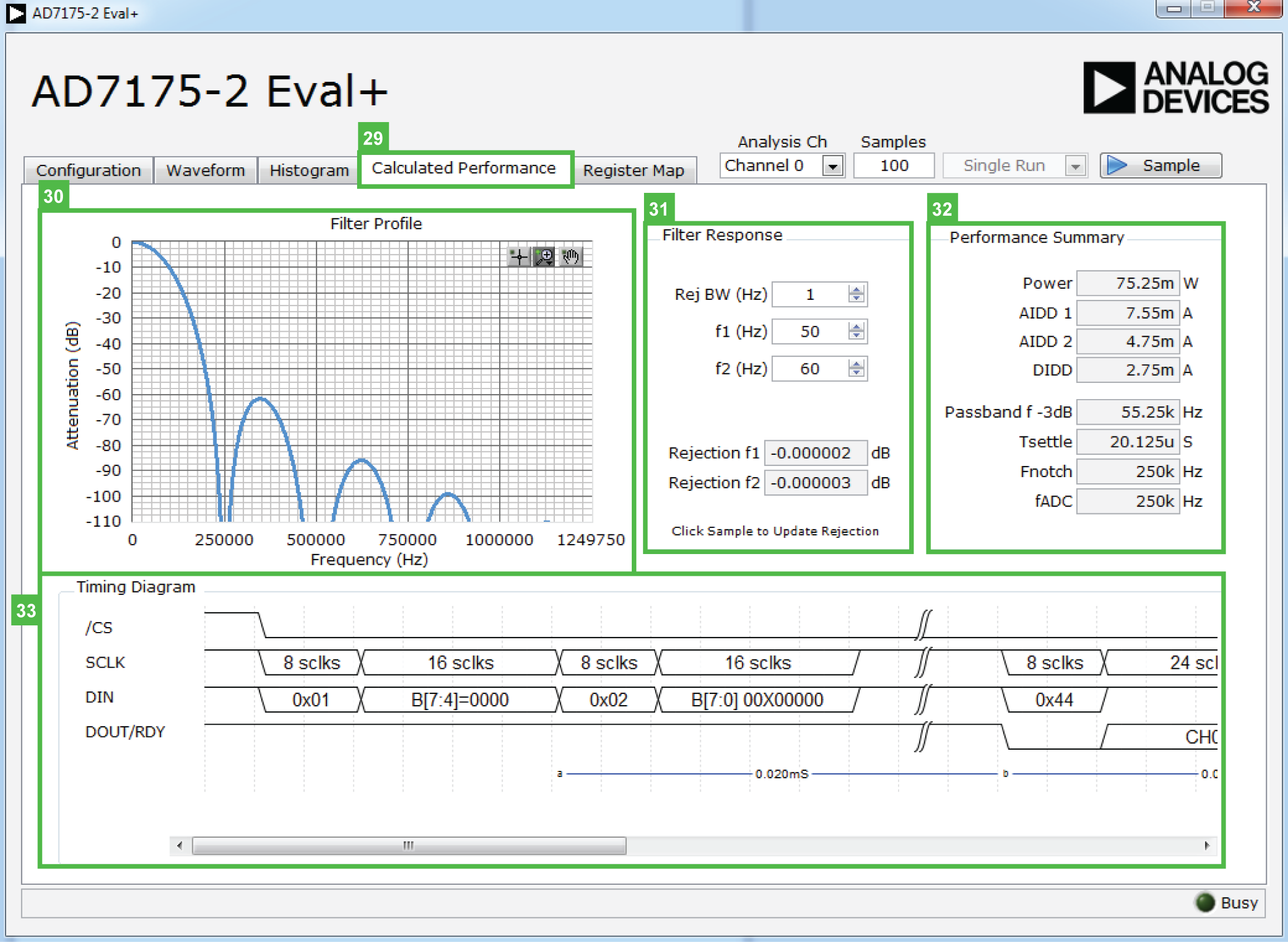
The Calculated Performance tab shows ADC performance parameters calculated using the ADC functional model. All results in the tab are for the current analysis channel (16).
Filter Profile & Response (30 & 31)
Shows a frequency response graph for the selected digital filter — the rejection/attenuation of the digital filter over the Rej BW for f1 and f2 in dB.
Performance Summary (32)
Shows the total power consumption of the part in the current configuration as well as the current consumption on each power supply rail. Also shows timing information about the currently selected output data rate (Tsettle, Fnotch, fADC).
Timing Diagram (33)
Shows the digital interface timing diagram for the current configuration, including timing for both the configuration of the ADC and subsequent data reads.
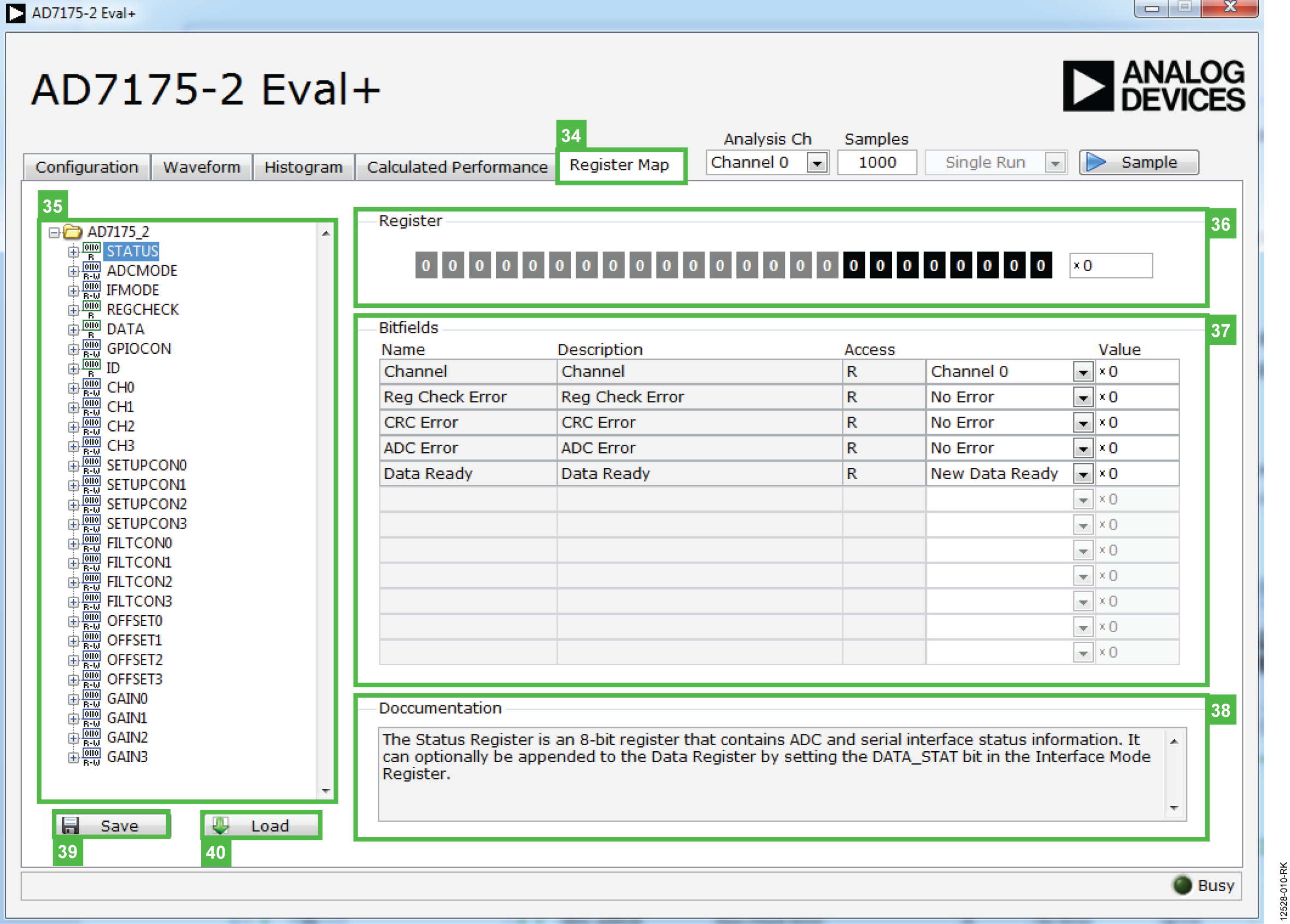
Register Map Tab
Register Tree (35)
Shows the full register map in a tree control. Each register is shown; clicking the expand button next to each register shows all the bit fields contained within that register.
Register Control (36)
Allows the user to change individual bits of the register selected in the register tree (35) by clicking on the bits or by programming the register value directly into the number control field.
Bit Field List (37)
Shows all the bit fields of the register selected in the register tree (35). Change values using the drop-down box or by directly entering a value into the number control field.
Documentation (38)
Contains the documentation for the register or bit field selected in the register tree (35).
Save and Load (39 and 41)
Allow the user to save the current register map setting to a file and to load a setting from the same file.
To exit the software, click the close button at the top right corner of the main window.