EVAL-AD717x User Guide
The AD717x family evaluation boards feature highly accurate, high resolution, multiplexed Σ-Δ ADCs with integrated analog input buffers, on-board power supply regulation, and an external amplifier section for amplifier evaluation. A 5V USB supply is regulated to the voltages required by the active device and its support components. The evaluation board connects to a PC via the SDP-K1 controller board using the Arduino headers.
Full specifications for each device are available in the respective product data sheet, which should be consulted when working with the evaluation board.
Features
Full-featured evaluation board for the AD717x family
PC control in conjunction with the SDP-K1 controller board
Standalone capability
Equipment Needed
AD717x evaluation board (see Prerequisites)
SDP-K1 controller board
DC signal source
USB cable
PC with USB 2.0 port
Device Description
The AD717x family comprises highly accurate, high resolution, multiplexed Σ-Δ ADCs designed for DC input signals. Depending on the specific device, these ADCs support 2 to 16 analog input channels in fully differential or pseudo-differential configurations. The maximum channel-to-channel scan rate is 50 kSPS (20 µs) for fully settled data. Output data rates range from 5 SPS to 250 kSPS. All devices include integrated analog input and reference buffers, an integrated precision 2.5 V reference, and an integrated oscillator.
Setup Procedures
After following the software installation instructions, set up the evaluation board and SDP-K1 board as follows.
Note
Software and drivers must be installed before connecting the evaluation board and SDP-K1 board to the USB port of the PC to ensure that the PC correctly recognizes the evaluation system.
Connect the SDP-K1 to the Arduino headers of the evaluation board.
Connect the SDP-K1 board to the PC using the USB cable.
Hardware Link Options
Note
Link options vary between boards. The table below is for the EVAL-AD7175-8ARDZ. Refer to the user manual of your specific evaluation board for the correct link configuration.
Link |
Default |
Description |
|---|---|---|
LK1 |
B |
Selects AVDD1 voltage. Position B: 5V supply. Position A: 3.3V from ADP150 (U6). Setting AVDD1 = 3.3V is not allowed when AVSS = −2.5V. |
LK2 |
B |
Selects AVDD2 voltage. Position B: 5V supply. Position A: 3.3V from ADP150 (U6). Setting AVDD2 = 3.3V is not allowed when AVSS = −2.5V. |
LK3 |
B |
Position B: internal clock output (default). Position A: crystal option. |
LK4 |
Inserted |
Inserted: connects REF− to AVSS. |
LK5 |
B |
Position B: REF+ connected to on-board 5V external reference (default). Position A: REF+ connected to 2.5V internal reference. |
LK6 |
A |
Position A: turns on LTC3129 (U3) to supply 7V to LDO linear regulators (default). Position B: turns off LTC3129 (U3). |
LK7 |
B |
Position A: shifts AVDD 5.5V to 7V. Position B: AVDD 5.5V set to 5.5V (default). |
LK8 |
A |
Position A: turns on ADP7118 (U10) to supply AVDD 5.5V (default). Position B: turns off ADP7118 (U10). |
LK9 |
A |
Position A: turns on 5V LDO (ADP7118 U11) to supply AVDD 5V (default). Position B: turns off ADP7118 (U11). |
LK10 |
A |
Position A: turns on 2.5V LDO (LT1962 U4) to supply AVDD 2.5V (default). Position B: turns off LT1962 (U4). |
LK11 |
A |
Position A: turns on LT1983 (U2) to supply ADP7182 (U5) 2.5V regulator (default). Position B: turns off LT1983 (U2). |
LK12 |
A |
Position A: turns on ADP7182 (U5) to supply −2.5V (default). Position B: turns off ADP7182 (U5). |
LK13 |
A |
Position A: turns on 3.3V LDO (ADP150 U6) to supply IOVDD 3.3V (default). Position B: turns off ADP150 (U6). |
LK14 |
Removed |
Insert when performing noise test. |
LK15 |
A |
Position A: connects REFOUT to VCM (default). Position B: connects REFOUT to A0. Remove when using external VCM from J15. |
LK16 |
B |
Position A: connects AIN0 to ADC driver. Position B: connects AIN0 directly to ADC (default). Remove when connecting AIN0 to surfboard. |
LK17 |
B |
Position A: connects AIN1 to ADC driver. Position B: connects AIN1 directly to ADC (default). Remove when connecting AIN1 to surfboard. |
LK18 |
A |
Position A: connects −VS to GND (default). Position B: connects −VS to −2.5V. Remove when using external supply. |
LK19 |
B |
Position A: connects +VS to AVDD 5V. Position B: connects +VS to AVDD 5.5V (default). Remove when using external supply. |
LK20 |
Inserted |
Inserted: initiates power-down for ADA4945/ ADA4940. Remove when using the ADC driver. Insert when performing noise test or when surfboard is connected. |
LK21 |
A |
Position A: connects SCLK to standard Arduino connection (default). Position B: connects SCLK to alternative Arduino connection for multiple boards. |
LK22 |
A |
Position A: connects DOUT to standard Arduino connection (default). Position B: connects DOUT to alternative Arduino connection for multiple boards. |
LK23 |
A |
Position A: connects DIN to standard Arduino connection (default). Position B: connects DIN to alternative Arduino connection for multiple boards. |
LK24 |
A |
Position A: connects CS to standard Arduino connection (default). Select a different position when stacking multiple boards. |
On-Board Connectors
Connector |
Function |
Type |
|---|---|---|
J1 |
External clock input or ADC internal clock output |
SMB Connector Jack, Male Pin 50Ω Through Hole Solder |
J2 |
External bench top voltage supply for AVDD 5V, AVDD 2.5V, AVSS −2.5V, and IOVDD |
Screw terminal block, 2.54 mm pitch |
J4 |
Arduino Headers (Power) |
8 Position Receptacle Connector, 2.54mm pitch |
J5 |
Arduino Header (Digital 1) |
10 Position Receptacle Connector, 2.54mm pitch |
J6 |
Arduino Header (Analog) |
6 Position Receptacle Connector, 2.54mm pitch |
J7 |
Arduino Header (Digital 0) |
8 Position Receptacle Connector, 2.54mm pitch |
J8 |
PMOD form factor |
12-pin header, 2.54mm pitch |
J9 |
Arduino Header (IFCSP) |
6 Position, 2 row, Receptacle Connector, 2.54mm pitch |
J15, J17 |
Analog input terminal block; wired connection to external source or sensor |
Power socket block, 8-pin, 2.54mm pitch, 3.5mm solder tail |
J16 |
Analog input terminal block; wired connection to external source or sensor |
Power socket block, 6-pin, 2.54mm pitch, 3.5mm solder tail |
J18 |
GPIO terminal |
4 Position 1 Row vertical PCB header, 2.54mm pitch |
J19 |
Surfboard header (optional) |
7-way, 2.54mm pin socket |
J20 |
Surfboard header (optional) |
7-way, 2.54mm pin header |
Power Supplies
The evaluation board receives power through the SDP-K1 controller board when connected to the PC via 5V USB. Linear regulators generate the required supply levels from the applied USB voltage. Each regulator can be individually shut down using its dedicated shutdown link.
AVDD1 and AVSS Selection (S1)
5V single supply (default): set S1 to SINGLE. The 5V regulator supplies AVDD1 and AVSS is tied to AGND.
±2.5V split supply: set S1 to SPLIT. The 2.5V regulator supplies AVDD1 and the −2.5V regulator supplies AVSS.
AVDD1 and AVDD2 Selection (LK1, LK2)
5V supply (default): set LK1 and/or LK2 to position B.
3.3V supply: set LK1 and/or LK2 to position A.
External AVDD/AVSS: set LK1, LK2, LK9, LK10, LK11, LK12, and LK13 to position B. For external AVDD only, set S1 to SINGLE and connect to pin 1 of J2. For external AVDD and AVSS, set S1 to SPLIT and connect to pins 2 and 3 of J2 respectively.
Supply |
Regulator |
Shutdown Link |
|---|---|---|
5V |
LK9 |
|
2.5V |
LK10 |
|
−2.5V |
LK12 |
|
3.3V |
LK13 |
Serial Interface
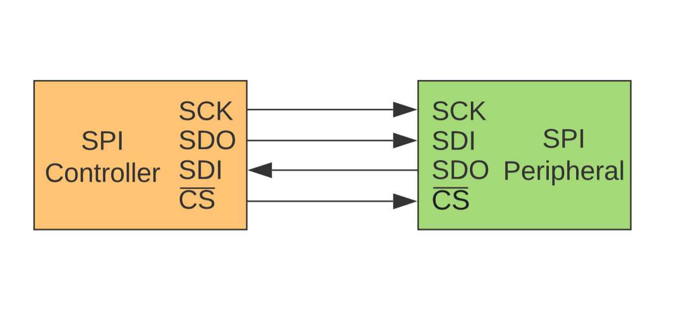
The evaluation board uses a 4-wire SPI interface: CS, SCLK, MOSI/DIN, and MISO/DOUT. It connects to any microcontroller board using the Arduino standard headers.
Serial communication options:
Arduino connection using the SDP-K1 (default)
PMOD connector (J8)
Standalone mode: remove LK21, LK22, LK23, and LK24, then use J5 to access all SPI signals directly
For an introduction to the SPI interface, see Introduction to SPI Interface.
Analog Inputs
Primary analog inputs are connected via J15, J16, and J17 on the left side of the board. Differential analog inputs are applied on AIN0 and AIN1 when using the ADC driver (enable AIN+/− buffers in this case). The input buffers are suited for DC input signals.
Reference Options
The following reference sources are available:
Internal 2.5V reference (on-chip)
Default: on-board external reference (ADR4550)
External reference via J17 through AIN1/REF2+ and AIN0/REF2− pins
Selecting the Reference Source (Hardware)
Link |
Default |
Description |
|---|---|---|
LK4 |
Inserted |
Inserted: connects REF− to AVSS. Removed: disconnects REF− from AVSS. |
LK5 |
B |
Position A: connects REF+ to REFOUT. Position B: connects REF+ to on-board ADR4550 external reference. |
Schematic, PCB Layout, Bill of Materials
Refer to the product page of your specific evaluation board on analog.com to download the design files.